 Ziang Chen1,2,3
 Guofu Zhang3
 Hao Cai1,2,3
 Christopher Bengel4
 Feng Liu5Xianyue Zhao1,2,3Shahar Kvatinsky6Heidemarie Schmidt1,2Rainer Waser4,5,7
 Stephan Menzel5*Nan Du1,2,3*
- 1Institute for Solid State Physics, Friedrich Schiller University Jena, Jena, Germany
- 2Department of Quantum Detection, Leibniz Institute of Photonic Technology (IPHT), Jena, Germany
- 3Department of Electrical Engineering and Information Technology, Technical University of Chemnitz, Chemnitz, Germany
- 4Institute of Materials in Electrical Engineering and Information Technology, RWTH Aachen University, Aachen, Germany
- 5Peter Grünberg Institut (PGI-7), Forschungszentrum Juelich GmbH, Juelich, Germany
- 6Andrew and Erna Viterbi Faculty of Electrical and Computer Engineering, Technion-Israel Institute of Technology, Haifa, Israel
- 7Peter Grünberg Institut (PGI-10), Forschungszentrum Juelich GmbH, Juelich, Germany
The high demand for performance and energy efficiency poses significant challenges for computing systems in recent years. The memristor-based crossbar array architecture is enthusiastically regarded as a potential competitor to traditional solutions due to its low power consumption and fast switching speed. Especially by leveraging self-rectifying memristive devices, passive crossbar arrays potentially enable high memory densities. Nonetheless, due to the lack of a switching control per cell, these passive, self-rectifying memristive crossbar arrays (srMCA) suffer from sneak path current issues that limit the range of accurate operation of the crossbar array. In this work, the sneak path current issues in the passive srMCAs based on self-rectifying bipolar and complementary switching memristive devices are comparatively analyzed. Under consideration of the worst-case scenario, three reading schemes are investigated: one wordline pull-up (OneWLPU), all wordline pull-up (AllWLPU), and floating (FL) reading schemes. As a conclusion, despite different switching dynamics, both types of self-rectifying memristive devices can efficiently suppress sneak path current in the srMCAs. In the FL reading scheme, the sneak path current flowing through the unselected reversely biased memristive cells in the srMCA can be considered as an accurate estimation for the practical sneak path current in the srMCA. By analyzing the sneak path current in the srMCAs with a size up to 64 × 64, it is demonstrated that the leakage current plays a crucial role for suppressing the sneak path current, and the sneak path current via an individual cell exhibits a continuous decrease while the accumulated total sneak path current in the unselected reverse biased region is increasing with expanding the crossbar size. The comparative study on the bipolar and complementary memristive devices based srMCAs under diverse reading schemes reveals the influence of the switching dynamics on the sneak path current effect in the srMCAs, and provides a beneficial reference and feasible solutions for the future optimization of the crossbar topology with the intention of mitigating sneak path effects.
1 Introduction
Recent cutting-edge applications in computing have highlighted the necessity for a shift from traditional computing to memory-centric computing (Jeon et al., 2021). In the traditional computing with the processor as central computing unit, the data to be processed is transferred from a discrete memory unit to the processor via a data bus, bringing the limitation on data throughput as the bottleneck of the traditional computing. The so-called von Neumann bottleneck causes transmission speed limitations, increased memory latency, and high power consumption (Backus, 1978). The memory-centric computing aims at addressing the bottleneck due to inherent computer design issues, by virtue of combining the processor together with the memory unit to avoid the data transmission via bus. Hence, the memory-centric computing overcomes the limitation of throughput and results in drastically improved energy efficiency (Gao et al., 2015; Amrouch et al., 2021). As one promising candidate to construct innovative memory-centric computing systems, the memristor has drawn much attention due to its nanoscale miniaturization (Hsieh et al., 2016; Du et al., 2017) and low-power consumption (Du et al., 2015; Chen et al., 2021). Especially for applications in neuromorphic computing that require intense computing, e.g., deep learning neural networks. The memristor-based crossbar topology has been proposed as a promising solution to construct the neural networks, due to its outstanding characteristics such as scalability, high switching performance, non-volatility, and low power consumption (Du et al., 2021a, 2015; Sun et al., 2020).
In recent works, the memristive crossbar arrays (MCA) are intensively studied with various typologies and different applications: 1-transistor-1-resistor (1T1R) (Li et al., 2018; Yao et al., 2020), 1-selector-1-resistor (1S1R) (Taylor et al., 2021), and 1-resistor (1R). In comparison to the 1T1R and 1S1R crossbar typologies, the 1R passive crossbar topology utilizes the self-rectifying switching behavior of the individual memristive cell to maintain its operational performance rather than relying on external devices, such as transistors and selectors that cause more power consumption (Li and Xia, 2019). Nevertheless, due to the lack of a switching control per cell, the self-rectifying memristor-based 1R crossbar architecture suffers from sneak path currents that limit the range of accurate operation of the crossbar array (Gül, 2019; Pi et al., 2019). The sneak path current is the current via the undesired paths, which are parallel to the intended path, when operating the MAC. As proposed by many references, e.g., (Linn et al., 2010; Li and Xia, 2019), etc., from a memory point of view, the actual performance of the MCA is evaluated by the read margin. The in-depth investigation of sneak path current contributes to understanding the variation of the read margins in the MCAs, which highlights the necessity of a sneak path current study in the 1R passive crossbar topology.
The reading operation in the passive MCAs based on the linear memristive devices has been investigated by Flocke et al., in 2007 (Flocke and Noll, 2007). It is demonstrated that the information reading from a passive MCA based on the linear memristive devices is extremely challenging due to unavoidable sneak path current issues, which can be addressed by introducing discrete devices, e.g., diodes (Wang et al., 2013) or threshold selectors (Park et al., 2015). As an alternative solution, self-rectifying memristive devices have been proposed to mitigate the sneak path issue without introducing external devices for successfully information reading from the passive MCAs (Li and Xia, 2019). Especially, the read margin analysis on the passive MCAs based on complementary memristive devices (Linn et al., 2010) has demonstrated their potential for depressing the sneak path effect and facilitating the application in large passive crossbar array architectures. Moreover, the emerging network structures with alternative operational mechanisms, which have good immunity to sneak path current issue, have been proposed (e.g., (Cui et al., 2022)).
In this paper, the sneak path effect is comparatively investigated in the 1R based passive srMCAs based on two memristive devices exhibiting the bipolar and complementary resistive switching dynamic, respectively. Under consideration of three different reading schemes, i.e., the one wordline pull-up (OneWLPU) scheme, the all wordlines pull-up (AllWLPU) scheme and the floating (FL) reading scheme, we concentrate on the analysis of the sneak path current in the srMCA, which is helpful to understand the changes in the read margin. In the worst-case scenario, the current in the unselected, reversed biased region in the FL reading scheme is confirmed as an accurate estimation for the overall sneak path current (but not in the OneWLPU scheme and the AllWLPU scheme), as proved by the simulation of the srMCAs in Cadence Virtuoso. The paper is organized as follows: after the introduction of the two self-rectifying memristive devices, i.e., bipolar and complementary switching memristors and their corresponding current-voltage (I-V) characteristics and mathematical models in Section 2, the sneak path current in the n x m srMCA based on bipolar and complementary memristive devices is investigated, by exploiting HRS and LRS initialization and writing steps with three reading schemes (Section 3). Section 3.3 reveals the effect of the leakage current of the bipolar memristive devices on the sneak path current in the n x m srMCA. With the expansion of the srMCA size, the accumulated total sneak path current in the unselected, reversed biased region exhibits a continuous heightening tendency, as confirmed by the simulation results in Section 3.3.
2 Electrical characterization of the Mem-BFO and Mem-BiBFO devices
2.1 Mathematical matching models of the Mem-BFO and Mem-BiBFO
In this paper, the BiFeO3 (BFO) memristive device exhibiting the bipolar resistive switching dynamic and the BiFeTiO3/BiFeO3 (BiBFO) memristive device exhibiting the complementary resistive switching dynamic are introduced. The srMCAs based on the bipolar BFO and complementary BiBFO memristive devices are comparatively investigated and analyzed. The schematic sketch of the Au-BFO-Pt/Ti metal-isulator-metal (MIM) structure for thr bipolar BFO memristive device (Mem-BFO) is depicted in the inset of Figure 2A. In comparison to the bipolar Mem-BFO, the complementary BiBFO memristive device (Mem-BiBFO) is provided with the structure of Au-BFO-BFTO-Pt/Ti with an additional BFTO layer, as exhibited in the inset of Figure 2B.
To fabricate the Mem-BFO devices, the polycrystalline BFO thin film with the thickness of 500 nm was deposited by pulsed laser deposition (PLD) on a Pt/Ti/SiO2/Si substrate with 100 nm/50 nm thick Pt/Ti layer, as in our previous work (Jin et al., 2014; You et al., 2014a). Circular Au top electrodes with an area of 105μm2 and a thickness of 150 nm were fabricated by DC magnetron sputtering at room temperature using a metal shadow mask. By exploiting the device’s highly uniform switching performance with excellent endurance and retention properties (Du et al., 2018; Shuai et al., 2018), the Mem-BFO has drawn much attention and has been applied in the research fields of neuromorphic computing (Du et al., 2021b; a, 2015), reconfigurable Boolean logic (You et al., 2014b; Zhou et al., 2015) and in hardware security (Du et al., 2014; Chen et al., 2021). With the intention of applying the Mem-BFO in-depth in various fields, a mathematical model for the Mem-BFO device has been developed and verified with experimental current-voltage switching characteristic (Cederström et al., 2013). In this work, the mathematical matching model for Mem-BFO (Cederström et al., 2013) is implemented by Verilog-A in the Cadence Virtuoso, and further adapted to model the complementary Mem-BiBFO device. The equations and the corresponding parameter set applied in this work are shown in Figure 1.
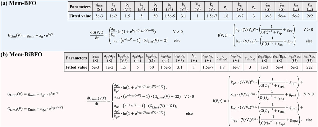
FIGURE 1. Behavioral mathematical model for (A) the bipolar Mem-BFO device and (B) the complementary Mem-BiBFO device. The simulation parameters are given in the corresponding tables as insets.
The I-V characteristics of the Mem-BFO and Mem-BiBFO devices are modeled as a system of equations containing a state variable G, a voltage-dependent limit of the state variable GLim, and the relationship between G, voltage and current. The state variable G represents the conductance of the memristive device, which is varied by the voltage and the time. The voltage dependent limit of the state variable GLim is a simple exponential function, and the saturation follows the basic principle G = a ⋅ (GLim − G). In the Mem-BFO model, the logarithmic function restricts the derivative to non-negative values for a positive voltage bias, whereas for negative voltages the exponential function acts as threshold for switching. In the Mem-BiBFO device, the hysteretic behavior can be found both in the positive bias range AND the negative bias range. Hence, in the corresponding matching model for the Mem-BiBFO, two complementary GLim conditions are adopted for restricting the current values in both bias ranges. In the model for the Mem-BiBFO, the modelling equations in the negative bias range are defined as a mirror image of the equations in positive bias range. In the mathematical models of the Mem-BFO and Mem-BiBFO, the various parameters endow different switching dynamics for the modeled memristive device as follows: ag and bg limit the maximum conductance possible for the Mem-BFO, which indicates the overall conductivity; kn and kp scale current level respectively at negative bias range and positive bias range, which indicates the barrier height at the top electrode (TE) region and bottom electrode (BE) region of the memristive device; rs and gp express two parasitic resistors in the memristive models, etc. All parameters utilized in the mathematical equation and their corresponding fitted values are listed in the table of Figure 1. The different simultaneous equations in positive and negative bias ranges provide the self-rectifying switching behavior of the Mem-BFO and Mem-BiBFO device as confirmed by the current-voltage characteristics shown in Figure 2.
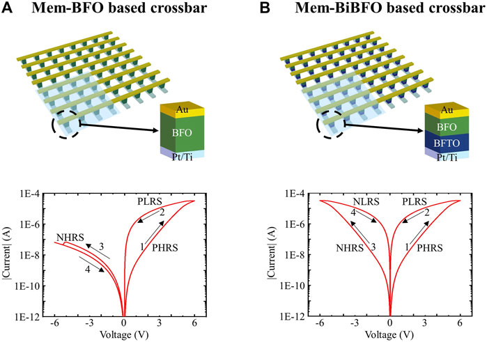
FIGURE 2. Three-dimensional geometric topology of the crossbar array based on (A) the bipolar Mem-BFO with the schematic sketch of the Au-BFO-Pt/Ti MIM structure and (B) the complementary Mem-BiBFO with the Au-BFO-BFTO-Pt/Ti MIM structure. Under the ramping triangular sourcing voltage with 6 V amplitude and 0.25 Hz ramping frequency, the simulated bipolar and complementary I-V characteristics of the individual Mem-BFO and Mem-BiBFO are stimulated. The arrows indicate the switching direction.
2.2 I-V characteristics of the Mem-BFO and Mem-BiBFO cells in the passive crossbar
The aforementioned mathematical models of the Mem-BFO and Mem-BiBFO are adopted in a passive crossbar topology for investigating the sneak path issue. Due to the self-rectifying characteristics of the Mem-BFO and Mem-BiBFO devices, a passive crossbar structure without any transistors is targed, i.e., srMCAs. This topology provides a higher memory density than the 1T1R crossbar topologies (Li and Xia, 2019). All simulations are performed in the Cadence Virtuoso.
Under the ramping source voltage, i.e., 0 V → 6 V → -6 V → 0 V, the Mem-BFO and the Mem-BiBFO in the 4 × 4 srMCA exhibit the bipolar and complementary rectifying switching dynamics, respectively, as demonstrated in Figure 2 with the direction of the currents flowing through memristive devices: 1 → 2 → 3 → 4. By applying large positive input bias, e.g., +6 V, to the Au TE of the Mem-BFO, the device is switched to the low resistance state (LRS), i.e., low resistance state in positive bias range/high resistance state in negative bias range (PLRS/NHRS). This process is identified as SET process, thus the PLRS or NHRS resistance state can be recorded respectively at the small reading bias, i.e., +2 V or −2 V. By sourcing large negative input voltage, e.g., −6 V, to the Au TE, the Mem-BFO can be then switched to the high resistance state (HRS), i.e., high resistance state in positive bias range/high resistance state in negative bias range (PHRS/NHRS), and the switching process is identified as RESET process. Thus, the PHRS or NHRS resistance state can be recorded respectively at the small reading bias, i.e., +2 V or −2 V. In comparison to the Mem-BFO, the Mem-BiBFO locates in the HRS, i.e., PHRS/NLRS, by sourcing large negative input voltage, e.g., −6 V, to the Au TE. By applying large positive input bias, e.g. +6 V, to the Au TE of Mem-BiBFO, the Mem-BiBFO is switched to LRS, i.e., PLRS/NHRS, as with the Mem-BFO. As revealed in Figure 2A, the analog hysteresis is recognizable within the positive bias range in the I-V characteristics of the Mem-BFO. It reveals the bipolar self-rectifying nonlinear switching behavior of the Mem-BFO. The mechanism of the bipolar resistive switching observed in BFO thin films can be explained by the modification of the Schottky barrier at the BFO-Pt bottom interface by the drift of charged oxygen vacancies under applied large electric fields during the writing step (You et al., 2015; Du et al., 2018). During the fabrication process by PLD, due to the high temperature, the Ti from the BE diffused into the BFO layer close to the BE region (You et al., 2014a). The Schottky barrier height at the BFO/Pt interface is influenced by the diffusive Ti4+ in the BFO oxide layer, i.e., fixed substitutional donors. Hence, the flexible Schottky barrier height resulting from the trapping and detrapping of mobile oxygen vacancies by the fixed substitutional donors under the positive or negative writing bias to the TE contributes to the particular excellent retention property of the Mem-BFO with the bipolar I-V characteristic. For the Mem-BiBFO, the analog switching hysteresis exists within both positive and negative bias ranges in the I-V characteristics, which indicates the complementary self-rectifying nonlinear switching behavior of the Mem-BiBFO, as illustrated in Figure 2B. The complementary I-V characteristic in the Mem-BiBFO is caused by the both flexible Schottky barrier height resulting from the drapping and detrapping of mobile oxygen vacancies by the fixed substitutional donors close to BE region and TE region.
In the following section, an srMCA with a size of 4 × 4, highlighted in Figure 2 with blue background, is selected as the starting point to investigate the sneak path current issues under various initialization conditions and reading schemes. Subsequently, the srMCA is extended up to 64 × 64. The following assumptions are adopted while investigating the sneak path current issue in the srMCAs based on Mem-BFO and Mem-BiBFO: 1) Cycle-to-cycle (C2C) and device-to-device (D2D) variability in the Mem-BFO and Mem-BiBFO device are neglected. 2) In the complementary I-V characteristics of the Mem-BiBFO, the PLRS in the positive bias range and the NLRS in the negative bias range are considered identical. In fact, the PLRS and NLRS in the I-V characteristics of the Mem-BiBFO are slightly asymmetric with respect to the voltage polarity due to the different Schottky barrier heights at the TE and BE interfaces. During the srMCA simulation, the modeling parameters are intentionally modified for generating identical PLRS and NLRS in the complementary I-V characteristics to avoid the influence of imperfect symmetry of the PLRS and NLRS in the I-V characteristics in the Mem-BiBFO on the sneak path current evaluation.
3 Bitmap analysis of the Mem-BFO and Mem-BiBFO based srMCAs
3.1 Operational procedure for the HRS and LRS initialization
As shown in the srMCAs of the m x n dimension with the 1R configuration in Figure 3 (m = n = 4), the self-rectifying memristive cells are arranged in a passive matrix configuration, in which the TEs on each row of the memristive matrix are connected together laterally and the BEs on the each column of the memristive matrix columns are assembled together longitudinally. The utilized orthogonal wires, are termed as wordlines (WLs), i.e., the horizontal intersecting lines, and as bitlines (BLs), i.e., the vertical intersecting lines, respectively. In the 1R configuration, no transistor is applied in series with each memristive cell. There are three operational steps applied on the passive srMCAs for evaluating the sneak path current: initialization, writing, and reading.
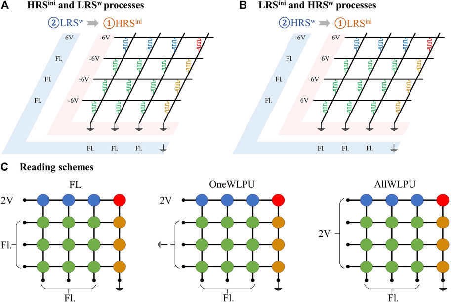
FIGURE 3. Distribution of the sourcing voltage on the 4 × 4 crossbar topology (A) for writing the red selected cell to the LRS (LRS w writing step) after the HRS initialization for each cell (HRS ini initialization step) and (B) for the HRS w writing step after the LRS ini initialization step. The wire resistances with the value of 10 Ω between each TE of the memristive cells on the WLs and between each BE of the memristive cells on the BLs are practically added to the srMCA simulation, despite the wire resistances are not drawn in the srMCA. (C) Comparison of the sourcing voltage on three reading schemes, i.e., FL, OneWLPU, and AllWLPU reading scheme, with identical sourcing voltage on the BLs and corresponding sourcing voltage on the unselected WLs: maintaining floating in the FL reading scheme, grounded in the OneWLPU reading scheme, and 2 V in the AllWLPU reading scheme.
The initialization step is classified into the HRS-initializing (HRS ini) and LRS-initializing (LRS ini). In the HRS ini, all of the memristive devices in the srMCA are switched to the HRS by applying large negative input bias, e.g., −6 V, to the Au TEs via the WLs, while maintaining the BLs grounded, as illustrated in Figure 3A with red background. In the LRS ini, by sourcing large positive input voltage, e.g., +6 V, to the WLs and holding the BLs grounded, all memristive devices are then switched to the LRS, as revealed in Figure 3B with red background.
In the writing step, the memristive device in the upper right corner of the srMCA is activated as the worst-case scenario. Due to the furthest physical distance from the voltage sources on the WL and the BL, the selected memristive cell suffers from the largest parasitic wire resistance in the worst-case scenario. All remaining unselected memristive cells in the srMCA still maintain the initial resistance state, which is the opposite resistance state of the selected memristive cell. After the HRS ini initialization step, the LRS w writing step is applied, whereas the LRS ini initialization step is followed by the HRS w writing step. In such worst-case scenario, it is most challenging to record distinguishable HRS and LRS at the selected cell by virtue of the maximized parasitic leakage current through the unselected memristive cells. It means, the worst-case scenario exposes the lowest performance limitation of the accurate operating range in the crossbar topology. Hence, in this work, the srMCA is studied in the worst-case scenario.
Figure 3A illustrates the applied voltage schemes for the HRS ini and LRS w. In the LRS w writing step as exhibited in Figure 3A with blue background, the selected memristive cell is individually switched to the LRS by utilizing +6 V on the corresponding selected WL and ground at the selected BL with all the remaining unselected WLs and BLs maintaining floating for the purpose to alleviate the sneak path current. Figure 3B illustrates the applied voltage biases on the WLs and the BLs for the LRS ini and HRS w. In the HRS w writing step, the selected memristive cell is individually reversed to the HRS assisted by applying −6 V on the corresponding selected WL and ground to the selected BL. All unselected WLs and BLs are kept floating. Upon the application of the HRS w and LRS w, the studied reading schemes are classified into three different topological patterns: the OneWLPU, FL, and AllWLPU reading scheme, according to the applied voltage biases on the unselected WLs as demonstrated in Figure 3C. The OneWLPU reading scheme features uncomplicated implementation and low power consumption, which is the most widespread reading scheme in circuitry implementation (Kim et al., 2015). In the OneWLPU reading scheme, the recorded data in the selected memristive device is extracted by applying a 2 V reading bias on the selected WL and ground at the selected BL, while the unselected WLs are grounded and the unselected BLs are kept floating. In comparison to the OneWLPU reading scheme, the FL reading scheme diminishes the sneak path current by virtue of floating the unselected WLs. In the AllWLPU reading scheme, the sneak path current is further declined by applying 2 V reading voltage on the unselected WLs. Nevertheless, simultaneously applying 2 V reading voltage on all WLs inevitably enhances significantly the power consumption.
3.2 Analysis of bitmaps for the srMCAs based on Mem-BFO and Mem-BiBFO
For investigating the sneak path effects, the HRS ini/LRS w and LRS ini/HRS w processes demonstrated in Figure 3 are performed in the srMCAs based on the bipolar Mem-BFO and complementary Mem-BiBFO.
In the HRS ini initialization step, the voltage value over each memristive cell in the 4 × 4 srMCAs based on the Mem-BFO and Mem-BiBFO amounts to −6 V, and the current values amount to −6.48 ⋅ 10–8 A and −1.53 ⋅ 10–5 A, respectively. Conversely, in the LRS ini initialization step, the voltage value over each memristive cell in both 4 × 4 srMCAs amounts to +6 V, and the current value amounts to 1.53 ⋅ 10–5 A.
After the initialization step, the LRS w and HRS w writing steps are implemented on the selected memristive cell in the top right corner. In Figure 4, the corresponding voltage and current bitmaps from the srMCAs with size of 4 × 4 are recorded for the Mem-BFO based srMCA and Mem-BiBFO based srMCA, respectively. As demonstrated in Figures 4A, B, during the LRS w and HRS w writing steps, four voltage/current regions in the srMCA are recognizable according to the corresponding voltage/current colorbar: the selected cell, the semi-selected Region 1 (the intersection area of the WL1 and the BL1, 2, 3, as marked with blue circle), the unselected Region 2 (the intersection area of the WL2, 3, 4 and the BL1, 2, 3, as marked with green circle), and the semi-selected Region 3 (the intersection area of the WL2, 3, 4 and the BL4, as marked with brown circle). Note that the voltage and current values in the same region stay constant by virtue of omitting C2C and D2D variability in the Mem-BFO and Mem-BiBFO mathematical models.
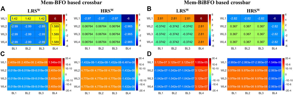
FIGURE 4. Simulated voltage/current bitmaps, located respectively in the top/bottom row, via each cell in the LRS w and HRS w writing steps based on bipolar Mem-BFO and complementary Mem-BiBFO: (A) and (B) are results for voltage bitmaps, (C) and (D) are results for current bitmaps. Four regions in the crossbar topology are established: selected cell, Region 1 with blue circle, Region 2 with green circle, and Region 3 with brown circle, where the voltage and current values in the same region sustain constant due to the lack of C2C and D2D variability in mathematical models of the memristive devices.
By applying writing voltages of +6 V and -6 V on the selected cell in the LRS w writing step and the HRS w writing step, the sneak path current is generated surrounding the selected cell from the selected WL to the grounded selected BL via numerous sneak paths. The flowing direction of sneak path current is indicated by the sign of the voltage/current values in the voltage/current bitmap of Figures 4A, B. Hence, e.g., in the LRS w writing step, the flowing direction of the sneak path current is revealed as the following sequence:
1) from the TE to the BE of the memristive cells in the semi-selected Region 1,
2) from the BE to the TE of the memristive cells in the unselected Region 2,
3) from the TE to the BE of the memristive cells in the semi-selected Region 3.
The existence of such sneak path that most intimates to the selected cell in the srMCA is verified by the voltage distribution in the voltage bitmap in both LRS w and HRS w writing steps in Figure 4A (Mem-BFO) and Figure 4B (Mem-BiBFO). For example, the sum of the absolute values in the three regions surrounding the selected cell amounts to the applied writing bias on the selected cell, e.g. in the LRS w writing step of the Mem-BFO based srMCA in Figure 4A: |+6 V| = |+1.42 V| + |-2.99 V| + |+1.59 V|.
As shown in Figure 4A for the Mem-BFO based srMCA, the voltage values in Region 2 in the LRS w writing step exceed the voltage values in Region 2 in the HRS w writing step significantly. This effect is due to the initialized NHRS and PLRS in memristive cells in Region 2 under negative and positive biases, respectively. In comparison to that, in the Mem-BiBFO based srMCA, the absolutely voltage values under the LRS w writing step in Figure 4B in all four regions are relatively close to the absolute voltage values under the HRS w writing step, which is caused by the initialized NLRS and PLRS in memristive cells in Region 2 under negative and positive biases, respectively.
By applying writing voltage of +6 V and −6 V on the selected cell in the LRS w and HRS w writing steps, respectively, in both srMCAs based on the Mem-BFO and Mem-BiBFO, the highest absolute writing current is located on the selected cell in the upper right corner of the srMCA, as illustrated in the current bitmaps of Figures 4C, D. As demonstrated in the current bitmaps of the LRS w and HRS w in the srMCAs based on the Mem-BFO and Mem-BiBFO in Figures 4C, D, respectively, the current values in Region 1 and Region three are equal to each other, attributable to the symmetric crossbar circuit topology. As the minimum current value in the corresponding current bitmap, the reverse current in Region 2 restricts the sneak path current in general, which indicates the bottleneck of the sneak path current. However, as demonstrated in Figure 4D, the current values in Region 2 in the Mem-BiBFO based srMCA in the LRS w and HRS w significantly exceed that in the Mem-BFO based srMCA. In the LRS w writing step, the Mem-BiBFO cells in Region 2 are in the NLRS, while the Mem-BFO cells located in Region 2 are in the NHRS. Therefore, despite the higher voltage value in Region 2 applied to the Mem-BFO cells than to the Mem-BiBFO cells, the current value in Region 2 is higher in the Mem-BiBFO cells. In the HRS w case, the Mem-BFO cells and the Mem-BiBFO cells in Region 2 are switched to PLRS. Hence, the higher writing current in Region 2 of the Mem-BiBFO cells compared to the Mem-BFO cells is generated by the larger voltage drop in Region 2 on the Mem-BiBFO cells.
Upon the application of the HRS ini/LRS w and LRS ini/HRS w processes, the current through individual cells in each region is recorded sequentially by using the three different reading schemes: FL, OneWLPU, and AllWLPU, which have been demonstrated in Figure 3. As C2C and D2D are neglected in this study, the recorded voltage/current values through the individual cell of each Region is identical (Figures 4A, B). Hence, the representative voltage/current value of each Region is plotted with respect to the reading schemes: OneWLPU, FL and AllWLPU as illustrated in Figure 5. The voltage values in Figures 5A, B and the current values in Figure 5C and Figure 5D are recorded from the selected cell (red squares), Region 1 (blue up-pointing triangles), Region 2 (green circles), and Region 3 (orange down-pointing triangles).
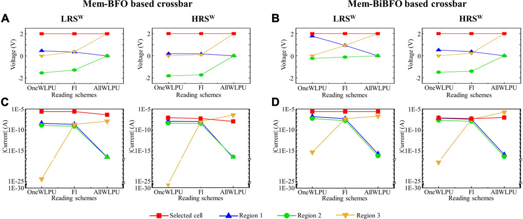
FIGURE 5. Comparison of the voltage/current values in the Mem-BFO and Mem-BiBFO based crossbars upon LRS w and HRS w writing steps with respect to three different reading schemes. (A) and (B) are results for voltage values. (C) and (D) are results for current values. The absolute current in Region 2 reveals the bottleneck of the sneak path current in the FL reading scheme, indicating its potential to act as an accurate estimation for the sneak path effect.
As indicated in Figures 5A, B, the reading voltage on the selected cell amounts to 2 V in each reading scheme by virtue of sourcing 2 V on the selected WL according to the distribution of applied sourcing voltage demonstrated in Figure 3C. Despite the wire resistances with the value of 10 Ω between each TE of the memristive cells on the WLs and between each BE of the memristive cells on the BLs have been practically added to the srMCA simulation, the total wire resistances (amount to 40 Ω) connected to the TE and the BE of the selected memristive cell in the 4 × 4 srMCA are negligible, in comparison to the resistance of the selected memristive cell, i.e., 45 MΩ at the HRS and 0.9 MΩ at the LRS. Hence, in the 4 × 4 srMCA simulation, the voltage drop on the selected memristor cell amounts to 2 V in the three reading schemes, as demonstrated in Figures 5A, B. The voltage value of each region depends on the applied sourcing voltages in diverse reading schemes and the resistance states of each memristive cell, which has been defined in the initialization and writing steps. As demonstrated in Figures 5A, B, the voltage values in Region 2 and Region three are raising in the Mem-BFO and the Mem-BiBFO based srMCAs with respect to the reading schemes: OneWLPU, FL, and AllWLPU as depicted on the x-axis. In contrast, the voltage value in Region 1 is declining.
Due to the resistance state PHRS/NLRS in the Mem-BiBFO in the semi-selected and the unselected memristive cells as illustrated in Figure 2B, the voltage values recorded from the Mem-BiBFO based srMCA after the LRS w is not only different from the case of the Mem-BiBFO based srMCA under the HRS w, but also from the cases of the Mem-BFO based srMCAs after the HRS w and LRS w. The Mem-BiBFO cells after the LRS w lie in NLRS under the negative voltage bias, whereas the Mem-BiBFO cells after the HRS w and the Mem-BFO cells (after the HRS w OR LRS w) lie in NHRS under the negative voltage bias. This difference in the resistance state of devices under the negative bias range results in such special voltage distribution.
The current bitmap in each region with respect to the OneWLPU, FL, and AllWLPU reading schemes are illustrated in the corresponding lower sub-diagrams in Figure 5C (Mem-BFO) and Figure 5D (Mem-BiBFO). In the srMCA simulation, after the application of the writing steps, the current through each memristive cell is recorded sequentially by utilizing the three different reading schemes in the order of FL → OneWLPU → AllWLPU. Hence, the resistive states of the selected memristive cells depend on the order in which the reading schemes are applied, leading to the nonidentical recorded current through the selected cell in the three reading schemes, as demonstrated in Figures 5C, D. Nevertheless, despite being affected by the order of applying the reading schemes, the differences in the recorded current in LRS and in HRS of the selected cells can be distinguished.
The read current values in Region 1 and Region 2 show a persistent downward trend in both type of the srMCAs for the LRS w and HRS w, which indicates the continuously suppressed sneak path effect while modifying the reading schemes. Conversely, the read current in Region three exhibits a continuing upward trend in both srMCAs, due to the extreme impact by the sourcing/connecting possibilities in the unselected WLs in different reading schemes. In the OneWLPU and AllWLPU reading schemes, the voltage difference between the TE and the BE of the cells in Region three amounts to 0 and 2 V, respectively. Applying 2 V on the selected cell excites the maximum read current on the selected cell after the LRS w writing for both srMCAs, whereas after the HRS w writing, the maximum read current occurs in Region 3 with the AllWLPU reading scheme. Such maximum read current in Region 3 after the HRS w writing is obtained as the memristive cells in Region three are at the PLRS while the selected cell is at the PHRS. Hence, under identical 2 V reading voltage values on the selected cell and the cells in Region three in the AllWLPU reading scheme, more current flows through the memristive cells in Region three than through the selected cell, which leads to the incorrect reading operation in the AllWLPU reading scheme. Note that, in the circuit design for reading information from the srMCA, the total current via the selected BL is extracted by a sensing amplifier that is connected to the selected BL, under the worst case scenario. In the AllWLPU reading scheme, the sensing current via the selected BL is dominated by the current via the selected cell and via the cells in Region 3, by applying 2 V to all WLs. Hence, the sensing current via the selected BL after the HRS w writing (i.e. dominated by the current via the selected HRS cell and via the initialized LRS cells in Region 3) is more pronounced than the sensing current after the LRS w writing, (i.e. dominated by the current via the selected LRS cell and via the HRS cells in Region 3), leading to a read failure. In such case, the sneak path current in Region 1 and Region 2 are strongly depressed, due to the voltage response in Region 1 and Region 2 close to 0 V.
Table 1 summarizes the current through the selected cell (Iselected cell) and the total current (including the sneak currents) flowing through the selected BL (IBL) for the Mem-BFO and the Mem-BiBFO based srMCAs for all three reading schemes. The highest ratios between the readout current from the selected cell, i.e., the ratio of Iselected cell obtained for the LRS w and the HRS w patterns, are obtained in the FL reading scheme for both type of the srMCAs due to the depressed sneak path current in the FL reading scheme. In comparison to the Mem-BFO based srMCA, the current ratio of Iselected cell in the OneWLPU and the FL reading scheme in the Mem-BiBFO based srMCA is slightly reduced. The current ratio in the AllWLPU reading scheme, in contrast, strongly decreases due to the obvious enhancement of the sneak path current caused by the complementary switching dynamic of Mem-BiBFO device. Moreover, the ratio between the current recorded at the selected BL, i.e. IBL, are lower than one in the AllWLPU reading scheme for both srMCAs, indicating a read failure. The read failure results from the sneak current via the cells in region 3 as 2 V is applied to all WLs in the AllWLPU reading scheme. This sneak current dominates the IBL. Hence, the IBL in the HRS w case, which is mainly determined by the current through the initialized LRS cells in Region 3, is higher than the IBL in the LRS w case, which is comparable to the current through the selected cell Iselected cell. Furthermore, due to the high current in Region three in the FL reading scheme, the current ratio of IBL is significantly reduced in both type of the srMCAs, in comparison to the current ratio of Iselected cell. In contrast, the current ratios of Iselected cell and IBL are comparable in the OneWLPU reading scheme since all sneak path current flows through the unselected WLs instead of the selected BL.
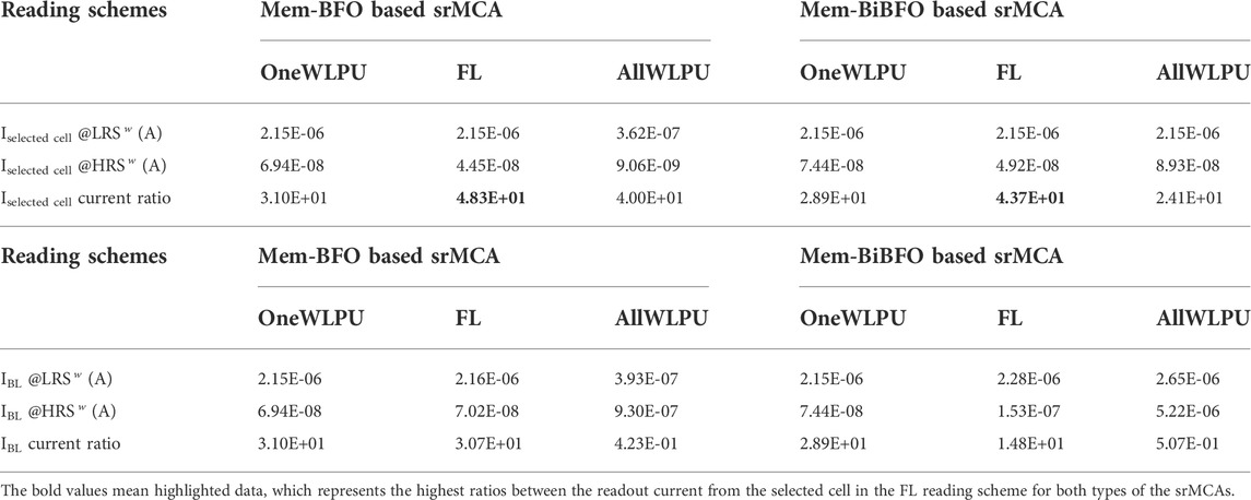
TABLE 1. Current values recorded via the selected cell (Iselected cell) and at the selected BL (IBL) in various reading schemes in both the Mem-BFO and Mem-BiBFO based srMCAs after the LRS w and HRS w writing steps.
As a conclusion, as revealed in Figures 5C, D, the absolute current values in Region 2 is the smallest in comparison to the other regions, which indicates the bottleneck of the sneak path current and it is capable of being considered as a most accurate estimation for the sneak paths effects. Despite the read failure in the AllWLPU scheme, it is illustrated that, due to the depressed sneak path current in the FL reading scheme, the ratio between the readout current from the selected cell in the LRS w and HRS w configuration is more pronounced in comparison to the OneWLPU reading scheme (Table 1). Nevertheless, due to the high current in Region 3 in the FL reading scheme, the current ratio between the current recorded at the selected BL, which is indicating the memory window of the srMCA, is significantly reduced in both the Mem-BFO and the Mem-BiBFO based srMCA.
3.3 Analysis of the sneak path issue in the srMCAs based on Mem-BFO up to 64 × 64
For exploring the influence of the leakage current in the negative bias range of the Mem-BFO cells on the sneak path effect in the implementation of the srMCAs, the sneak path current in the srMCA is recorded with various leakage current level of the individual cell. Figure 6A depicts the m x n dimension of the srMCA, where m equals n. The BL current values along the WL after each BL crossing 1 to n-1 are defined as ISC-BL(1) to ISC-BL(n-1), as marked with arrows in gradually darkening green in Figure 6A. The color gradient from light green to dark green represents the continuous accumulation of the current. The total current through the selected BL in the srMCA is defined as IBL and marked with a red arrow.
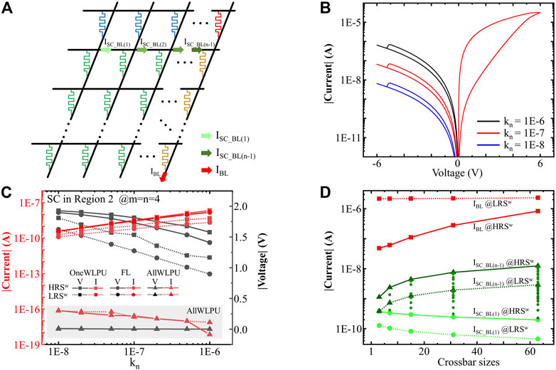
FIGURE 6. (A) Schematic sketch of sneak path current via the WLs and BLs in the srMCA with m x n dimension (m = n). The wire resistances with the value of 10 Ω between each TE of the memristive cells on the WLs and between each BE of the memristive cells on the BLs are practically added to the srMCA simulation, despite the wire resistances are not drawn in the srMCA. (B) Effect of the parameter kn in the mathematical model of the Mem-BFO on the negative leakage current in its I-V characteristic. (C) Sneak path current and voltage over each memristive cell in Region 2. The reading schemes of the OneWLPU (square), FL (circular), and AllWLPU (triangle) are considered after LRS w writing step (dashed lines) and HRS w writing step (solid lines). (D) The overall current via the selected BL (IBL in red) and sneak path current over the line resistors (ISC-BL(1), ISC-BL(2) …ISC-BL(n-1)) after each BLs (from light green to dark green) in dependence of crossbar sizes after the LRS w writing step (dashed lines) and HRS w writing step (solid lines). The FL reading scheme is considered and kn =10–8.
By modifying the parameter kn in the mathematical model of the Mem-BFO device, the leakage current at the negative bias range is modified. The maximum negative leakage current for the chosen values is achieved for kn = 1 ⋅ 10–6, as demonstrated in Figure 6B. Figure 6C reveals the relation between the sneak path current in Region 2 (red color) with respect to the modelling parameter kn (x-axis) for the three reading schemes. The square, circular, and triangular symbols represent the OneWLPU, the FL, and the AllWLPU reading scheme, respectively, after the LRS w (dashed lines) and HRS w case (solid lines). By modifying the parameter kn, the more pronounced leakage current in the negative bias range leads to the more apparent sneak path current in Region 2 in the OneWLPU and the FL reading schemes as revealed by the current curves with red color in Figure 6C. With increasing kn, the voltage difference between the TE and the BE of the memristive devices in Region 2 (black curves) shows a downward trend in the OneWLPU and the FL reading schemes. In all reading schemes, the reversed voltage biases are applied on memristive cells in Region 2 as demonstrated in Figure 5. Hence, in comparison to kn = 10–6, the resistance value with kn = 10–8 is significantly enhanced due to the lower leakage current under negative bias, which leads to a higher negative response bias in Region 2. As exhibited in Figure 6C, the voltage distribution on the Mem-BFO cells in Region 2 maintains 0 V, which leads to the negligible read current in the AllWLPU reading scheme. For investigating the sneak path effect in the srMCA with various array size from 4 × 4 up to 64 × 64, the parameter kn is set to 10–8 and the FL reading scheme is selected for obtaining the weakest sneak path current in Region 2, in comparison to the OneWLPU reading scheme. Furthermore, as demonstrated in Table 1, the highest current ratio of the two read current values via the selected cell in LRS w and HRS w configuration is located in the FL reading scheme in both srMCAs, signifying the advantage of the FL reading scheme. This result motivates choosing the FL reading scheme for further study.
As depicted in Figure 6D, the total current IBL through the selected BL in the FL reading scheme is shown as the red curves after the LRS w writing step (dashed line) and the HRS w writing step (solid lines). The rising trend of the IBL proves the enhancement of the total sneak path current with expanding the crossbar size. Such conclusion is consistent with the work in Ref. (Li and Xia, 2019), where more significant sneak path effect exists in the srMCA with 1M bits capacity, in comparison to the capacity of 10 bits. As demonstrated in Figure 6D, in comparison to the IBL for the LRS w configuration, the IBL for the HRS w configuration enlarges more obviously. After the LRS w writing step, the selected cell is switched to the LRS, where the reading current of the selected cell in the FL reading scheme dominates the IBL. Therefore, with the expanding of the crossbar size, the IBL is not affected by the enhanced sneak path current and remains identical. In comparison to the implementation of the srMCA with LRS w configuration, in the FL reading scheme after the HRS w writing step, the IBL is affected obviously by the enhanced sneak path current and depicts a persistent upward trend with the expanding of the crossbar size, as revealed in Figure 6D.
As mentioned in the previous description about the simulation result of the srMCA with size 4 × 4, the sneak path current flowing through each cell in Region 2 has been monitored, showing an identical value. For the purpose of an in-depth investigating of the sneak path effect in the srMCA, the currents via the WL after each BL crossing 1 to n-1, i.e. ISC-BL(1) to ISC-BL(n-1), are recorded. These currents are marked with arrows in gradually darkening green in Figure 6A. The color gradient from light green to dark green represents the continuous accumulation of the sneak path current on the unselected WL.
In the srMCA with various dimensions of m x n (from 4 × 4, 8 × 8 … up to 64 × 64), the sneak path current after each BLs with numbering from 1 to n-2, i.e. from ISC-BL(1) to ISC-BL(n-2), are recorded and marked with circular symbol and the triangle symbol represents the accumulated current on the WL, i.e. ISC-BL(n-1), in Figure 6D after two writing steps, i.e. the LRS w (dashed lines) and the HRS w (solid lines). As demonstrated in Figure 6D, under the same crossbar size, the accumulated current on each WL, i.e. ISC-BL(n-1), stays constant. With increasing BL numbering, the ISC-BL enhances, i.e. from ISC-BL(1) to ISC-BL(n-1), due to the continuously accumulating sneak path current on the corresponding WL. On the same WL in the srMCA, the ISC-BL(1) and the ISC-BL(n-1) indicate the weakest and most pronounced sneak path currents, as marked with lowest circular and triangle symbols in Figure 6D, respectively. By modifying the srMCA size from 4 × 4 to 64 × 64, after the HRS w and the LRS w writing steps, the accumulated sneak path current on the unselected WL, i.e., ISC-BL(n-1), depicts an persistent upward trend, which indicates the increasing sneak path current with increasing crossbar size. Nevertheless, the weakest sneak path current-ISC-BL(1)-exhibits a continuing downward trend with the increase of the crossbar size, which is caused by the diminution of the voltage drop over the single cells in Region 2.
4 Conclusion
In this work, the sneak path current issue is comparatively investigated in the 1R passive srMCAs based on bipolar and complementary memristive devices upon the application of the LRS w and HRS w writing steps. Under consideration of the worst-case scenario, three reading schemes are investigated: the OneWLPU, the AllWLPU, and the FL reading scheme. Despite the read operation failure in the AllWLPU reading scheme, the ratio between the read current from the selected cell under the LRS w and the HRS w configurations is more pronounced in comparison to the OneWLPU reading scheme due to the depressed sneak path current in the FL reading scheme. Furthermore, in the FL reading scheme, the current flowing through Region 2, i.e., the unselected, reversed biased region, is the smallest in comparison to the other regions, which indicates the bottleneck of all possible sneak paths within the srMCAs. Hence, it is capable of being considered as an accurate estimation for the practical sneak path current in both type of srMCAs. In comparison to the bipolar Mem-BFO based srMCAs, the sneak path effect is only slightly increased in the Mem-BiBFO based srMCAs, which indicates that the sneak path current is also efficiently depressed by the complementary switching dynamics of the Mem-BiBFO cells. By expanding the crossbar size of the Mem-BFO based srMCA up to 64 × 64, the accumulated sneak path current at the BL of the selected cell is strongly enhanced upon the HRS w configuration, whereas only slightly increased for the LRS w configuration, despite the sneak path current in the individual memristive cells in Region 2 is declining. Hence, it is concluded that the higher sneak path current in the larger scale of the srMCA results from the increased crossbar size with more prospect on sneak path possibilities.
A clear contribution of the study of the sneak path current issues of the 1R passive srMCAs in this work lies in providing an accurate understanding of the read margin by exploiting the sneak path current in the semi-selected and the unselected memristive regions without introducing external pull up resistances. The comparative sneak path current study in the bipolar and complementary memristor based srMCAs with diverse reading schemes offers a beneficial reference and feasible solutions for the future optimization of the srMCA designs with the intention of mitigating sneak path issues.
Data availability statement
The raw data supporting the conclusion of this article will be made available by the authors, without undue reservation.
Author contributions
All authors listed have made a substantial, direct, and intellectual contribution to the work and approved it for publication.
Funding
This work is supported by the German Research Foundation (DFG) Projects MemDPU (Grant Nr. DU 1896/3-1) and MemCrypto (Grant Nr. DU 1896/2-1). SM, FL and CB, acknowledge the funding support by the by the DFG under Grant SFB 917 and in part by the Federal Ministry of Education and Research (BMBF, Germany) through the project NEUROTEC II with the grant numbers 16ME0398K and 16ME0399. We acknowledge support by the Open Access Publication Fund of the Thueringer Universitaets-und Landesbibliothek Jena project no. 433052568.
Acknowledgments
The authors acknowledge Jan Pauliuk at TU Chemnitz for technical support on simulation tool Cadence Virtuoso and Matlab programming.
Conflict of interest
Authors FL, SM and RW are employed by Forschungszentrum Juelich GmbH.
The remaining authors declare that the research was conducted in the absence of any commercial or financial relationships that could be construed as a potential conflict of interest.
Publisher’s note
All claims expressed in this article are solely those of the authors and do not necessarily represent those of their affiliated organizations, or those of the publisher, the editors and the reviewers. Any product that may be evaluated in this article, or claim that may be made by its manufacturer, is not guaranteed or endorsed by the publisher.
References
Amrouch, H., Du, N., Gebregiorgis, A., Hamdioui, S., and Polian, I. (2021). “Towards reliable in-memory computing: From emerging devices to post-von-neumann architectures,” in 2021 IFIP/IEEE 29th International Conference on Very Large Scale Integration (VLSI-SoC), Nanyang Technological University Center, Singapore, October 4–8, 2021 (IEEE), 1–6.
Backus, J. (1978). Can programming be liberated from the von neumann style? a functional style and its algebra of programs. Commun. ACM 21, 613–641. doi:10.1145/359576.359579
Cederström, L., Stärke, P., Mayr, C., Shuai, Y., Schmid, H., and Schüffny, R. (2013). “A model based comparison of bifeo3 device applicability in neuromorphic hardware,” in 2013 IEEE International Symposium on Circuits and Systems (ISCAS), Beijing, China, May 19–23, 2013 (IEEE), 2323–2326.
Chen, Z., Du, N., Kiani, M., Zhao, X., Skorupa, I., Schulz, S., et al. (2021). Second harmonic generation exploiting ultra-stable resistive switching devices for secure hardware systems. IEEE Trans. Nanotechnol. 21, 71–80. doi:10.1109/tnano.2021.3135713
Cui, B., Fan, Z., Li, W., Chen, Y., Dong, S., Tan, Z., et al. (2022). Ferroelectric photosensor network: an advanced hardware solution to real-time machine vision. Nat. Commun. 13, 1707–1712. doi:10.1038/s41467-022-29364-8
Du, N., Manjunath, N., Shuai, Y., Bürger, D., Skorupa, I., Schüffny, R., et al. (2014). Novel implementation of memristive systems for data encryption and obfuscation. J. Appl. Phys. 115, 124501. doi:10.1063/1.4869262
Du, N., Kiani, M., Mayr, C. G., You, T., Bürger, D., Skorupa, I., et al. (2015). Single pairing spike-timing dependent plasticity in BiFeO3 memristors with a time window of 25 ms to 125 μs. Front. Neurosci. 9, 227. doi:10.3389/fnins.2015.00227
Du, C., Cai, F., Zidan, M. A., Ma, W., Lee, S. H., and Lu, W. D. (2017). Reservoir computing using dynamic memristors for temporal information processing. Nat. Commun. 8, 2204–2210. doi:10.1038/s41467-017-02337-y
Du, N., Manjunath, N., Li, Y., Menzel, S., Linn, E., Waser, R., et al. (2018). Field-driven hopping transport of oxygen vacancies in memristive oxide switches with interface-mediated resistive switching. Phys. Rev. Appl. 10, 054025. doi:10.1103/physrevapplied.10.054025
Du, N., Schmidt, H., and Polian, I. (2021a). Low-power emerging memristive designs towards secure hardware systems for applications in internet of things. Nano Mater. Sci. 3, 186–204. doi:10.1016/j.nanoms.2021.01.001
Du, N., Zhao, X., Chen, Z., Choubey, B., Di Ventra, M., Skorupa, I., et al. (2021b). Synaptic plasticity in memristive artificial synapses and their robustness against noisy inputs. Front. Neurosci. 696, 660894. doi:10.3389/fnins.2021.660894
Flocke, A., and Noll, T. G. (2007). “Fundamental analysis of resistive nano-crossbars for the use in hybrid nano/cmos-memory,” in ESSCIRC 2007-33rd European Solid-State Circuits Conference, Muenchen, Germany, September 11–13, 2007 (IEEE), 328–331.
Gao, M., Ayers, G., and Kozyrakis, C. (2015). “Practical near-data processing for in-memory analytics frameworks,” in 2015 International Conference on Parallel Architecture and Compilation (PACT), San Francisco, CA, USA, October 18–21, 2015 (IEEE), 113–124.
Gül, F. (2019). Addressing the sneak-path problem in crossbar rram devices using memristor-based one schottky diode-one resistor array. Results Phys. 12, 1091–1096. doi:10.1016/j.rinp.2018.12.092
Hsieh, C.-C., Roy, A., Chang, Y.-F., Shahrjerdi, D., and Banerjee, S. K. (2016). A sub-1-volt analog metal oxide memristive-based synaptic device with large conductance change for energy-efficient spike-based computing systems. Appl. Phys. Lett. 109, 223501. doi:10.1063/1.4971188
Jeon, K., Kim, J., Ryu, J. J., Yoo, S.-J., Song, C., Yang, M. K., et al. (2021). Self-rectifying resistive memory in passive crossbar arrays. Nat. Commun. 12, 1–15. doi:10.1038/s41467-021-23180-2
Jin, L., Shuai, Y., Ou, X., Siles, P., Zeng, H., You, T., et al. (2014). Resistive switching in unstructured, polycrystalline bifeo3 thin films with downscaled electrodes. Phys. Status Solidi A 211, 2563–2568. doi:10.1002/pssa.201431298
Kim, S., Kim, H.-D., and Choi, S.-J. (2015). Numerical study of read scheme in one-selector one-resistor crossbar array. Solid-State Electron. 114, 80–86. doi:10.1016/j.sse.2015.08.001
Li, C., and Xia, Q. (2019). “Three-dimensional crossbar arrays of self-rectifying si/sio 2/si memristors,” in Handbook of memristor networks (Springer), 791–813.
Li, C., Hu, M., Li, Y., Jiang, H., Ge, N., Montgomery, E., et al. (2018). Analogue signal and image processing with large memristor crossbars. Nat. Electron. 1, 52–59. doi:10.1038/s41928-017-0002-z
Linn, E., Rosezin, R., Kügeler, C., and Waser, R. (2010). Complementary resistive switches for passive nanocrossbar memories. Nat. Mater. 9, 403–406. doi:10.1038/nmat2748
Park, J., Cha, E., Lee, D., Lee, S., Song, J., Park, J., et al. (2015). Improved threshold switching characteristics of multi-layer nbox for 3-d selector application. Microelectron. Eng. 147, 318–320. doi:10.1016/j.mee.2015.04.045
Pi, S., Li, C., Jiang, H., Xia, W., Xin, H., Yang, J. J., et al. (2019). Memristor crossbar arrays with 6-nm half-pitch and 2-nm critical dimension. Nat. Nanotechnol. 14, 35–39. doi:10.1038/s41565-018-0302-0
Shuai, Y., Peng, Y., Pan, X., Jin, L., Wu, C., Luo, W., et al. (2018). Coexistence of memristive and memcapacitive effects in oxide thin films. Jpn. J. Appl. Phys. (2008). 57, 121502. doi:10.7567/jjap.57.121502
Sun, H., Luo, Z., Zhao, L., Liu, C., Ma, C., Lin, Y., et al. (2020). Bifeo3-based flexible ferroelectric memristors for neuromorphic pattern recognition. ACS Appl. Electron. Mater. 2, 1081–1089. doi:10.1021/acsaelm.0c00094
Taylor, B., Shrestha, A., Qiu, Q., and Li, H. (2021). “1s1r-based stable learning through single-spike-encoded spike-timing-dependent plasticity,” in 2021 IEEE International Symposium on Circuits and Systems (ISCAS), Daegu, Korea, May 22–28, 2021 (IEEE), 1–5.
Wang, G., Lauchner, A. C., Lin, J., Natelson, D., Palem, K. V., and Tour, J. M. (2013). High-performance and low-power rewritable SiOx 1 kbit one diode-one resistor crossbar memory array. Adv. Mater. 25, 4789–4793. doi:10.1002/adma.201302047
Yao, P., Wu, H., Gao, B., Tang, J., Zhang, Q., Zhang, W., et al. (2020). Fully hardware-implemented memristor convolutional neural network. Nature 577, 641–646. doi:10.1038/s41586-020-1942-4
You, T., Du, N., Slesazeck, S., Mikolajick, T., Li, G., Burger, D., et al. (2014a). Bipolar electric-field enhanced trapping and detrapping of mobile donors in bifeo3 memristors. ACS Appl. Mater. Interfaces 6, 19758–19765. doi:10.1021/am504871g
You, T., Shuai, Y., Luo, W., Du, N., Bürger, D., Skorupa, I., et al. (2014b). Exploiting memristive BiFeO3 bilayer structures for compact sequential logics. Adv. Funct. Mater. 24, 3357–3365. doi:10.1002/adfm.201303365
You, T., Ou, X., Niu, G., Bärwolf, F., Li, G., Du, N., et al. (2015). Engineering interface-type resistive switching in bifeo3 thin film switches by ti implantation of bottom electrodes. Sci. Rep. 5, 18623–18629. doi:10.1038/srep18623
Keywords: bipolar and complementary memristors, self-rectifying switching dynamic, crossbar array, sneak path current, reading scheme, worst-case scenario
Citation: Chen Z, Zhang G, Cai H, Bengel C, Liu F, Zhao X, Kvatinsky S, Schmidt H, Waser R, Menzel S and Du N (2022) Study on sneak path effect in self-rectifying crossbar arrays based on emerging memristive devices. Front. Electron. Mater. 2:988785. doi: 10.3389/femat.2022.988785
Received: 07 July 2022; Accepted: 14 September 2022;
Published: 04 October 2022.
Edited by:
Filippo Giannazzo, Department of Physical Sciences and Technologies of Matter, National Research Council (CNR), ItalyReviewed by:
Zhen Fan, South China Normal University, ChinaKB Jinesh, Indian Institute of Space Science and Technology, India
Copyright © 2022 Chen, Zhang, Cai, Bengel, Liu, Zhao, Kvatinsky, Schmidt, Waser, Menzel and Du. This is an open-access article distributed under the terms of the Creative Commons Attribution License (CC BY). The use, distribution or reproduction in other forums is permitted, provided the original author(s) and the copyright owner(s) are credited and that the original publication in this journal is cited, in accordance with accepted academic practice. No use, distribution or reproduction is permitted which does not comply with these terms.
*Correspondence: Nan Du, bmFuLmR1QHVuaS1qZW5hLmRl; Stephan Menzel, c3QubWVuemVsQGZ6LWp1ZWxpY2guZGU=