 Maurizio Burla1,2*
 Claudia Hoessbacher3Wolfgang Heni3Christian Haffner4Yannick Salamin5Yuriy Fedoryshyn2Tatsuhiko Watanabe2Hermann Massler6Tobias Blatter2Yannik Horst2
 Delwin L. Elder7,8Larry R. Dalton7Juerg Leuthold2*
- 1Institute of High Frequency Technologies and Photonics, TU Berlin, Berlin, Germany
- 2Institute of Electromagnetic Fields, ETH Zurich, Zurich, Switzerland
- 3Polariton Technologies Inc., Rüschlikon, Switzerland
- 4IMEC, Leuven, Belgium
- 5Research Laboratory of Electronics, MIT, Cambridge, MA, United States
- 6Fraunhofer IAF, Freiburg im Breisgau, Germany
- 7Department of Chemistry, University of Washington, Seattle, WA, United States
- 8NLM Photonics, Seattle, WA, United States
THz frequencies offer enormous amounts of bandwidth, which could solve the current speed bottleneck for next-generation wireless communications. Recent reports show sub-THz links offering capacities of hundreds of Gbit/s, finally approaching those of state-of-the-art optical transmission channels. Non-etheless, generation, transport, detection and processing of signals in the THz range is far from being a trivial task. Even though the recent evolution of integrated technology is starting to indicate that chip-scale THz technology could gradually close the so-called “THz gap,” much work still needs to be done to enable functional systems, in particular in terms of efficiency. Photonics can be of help, thanks to its extremely low loss and broad bandwidth. Yet, a particularly critical aspect hindering the deployment of THz technology is that state-of-the-art photonics devices generally do not offer sufficient electro-optical bandwidth to process THz signals. Plasmonics, by focusing electromagnetic surface waves at sub-wavelength scales, can play a key role in this quest, as it finally enables the realization of electro-optical devices such as modulators and detectors displaying sufficient compactness and speeds to reach the THz range. This paper overviews recent achievements on plasmonic-based modulators displaying characteristics of speed, efficiency and linearity that enable high-performance access to this much desired frequency range.
1 Introduction
The terahertz (100 GHz–10 THz) and in particular the sub-THz frequency range (up to 300 GHz) have experienced a major raise in interest in recent years. THz technologies offer a tremendous potential for multiple application domains, from high-volume wireless communications (5G and 5G+) (Seeds et al., 2015b), to sensing (Ren et al., 2019), security screening (Palka et al., 2014), non-invasive medical imaging (Brun et al., 2010), astronomy (Wang et al., 2019), and more (Yu et al., 2018). As examples, sub-THz frequencies were recently used in the ultra-high resolution interferometric radio astronomy observations that allowed to image, for the very first time, the shadow of the supermassive black hole in the center of the Milky Way (Akiyama et al., 2022). Besides unprecedented resolution in astronomical imaging, THz frequencies offer enormous amounts of bandwidth (Nagatsuma et al., 2016; Oxenløwe et al., 2018) that could solve the current speed bottleneck for next-generation wireless communications (Hecht, 2016).
In the past, this frequency range has been referred to as the “THz gap”, due to the lack of efficient methods to generate and detect signals at these frequencies. The recent evolution of integrated technology is starting to indicate that chip-scale THz technology could gradually close this gap (Sengupta et al., 2018; Shahramian et al., 2018). Nonetheless, much work still needs to be done to enable functional THz systems (Mittleman, 2013), which are still far from becoming efficient and practical.
Photonics technology, instead, allows low-loss transport of high frequencies, including THz, over large distances. As a reference, standard optical fibers losses can be as little as 0.2 dB/km. Yet, while excelling at low loss and broadband transport, the best photonic technologies to this date still struggle with the conversion of signals from the THz to the optical domains, which is a fundamental operation needed to experience the benefits offered by photonics transport of high-speed electrical signals.
Very recently, impressive progress has been made in fast and efficient lithium niobate modulators based on thin-film technology (Mercante et al., 2018; Wang et al., 2018; Weigel et al., 2018). Weigel et al. (2018) oxide-bonded a thin-film of LiNbO3 to a foundry-fabricated silicon photonic circuit and obtained a 3-dB bandwidth beyond 106 GHz. Mercante et al. (2018) fabricated a thin film crystal ion sliced (CIS) LiNbO3 phase modulator where, by very accurate index matching between the co-propagating modes (optical and RF) an electro-optical response up to 500 GHz could be measured, with a Vπ,DC of 3.8 V/cm. Wang et al. (2018) have shown lithium niobate-on-insulator (LNOI) Mach–Zehnder optical modulators with a 3-dB bandwidth of 100 GHz and a VπL of 2.2 V cm, and also a 40 GHz bandwidth, 20 mm-long device with a loss of only 0.5 dB and an ultra-low RF half-wave voltage of 1.4 V. All these devices show very strong potential for microwave photonic systems and next-generation optical communication networks. But while the fastest photonic modulators displayed measurable sidebands at sub-THz frequencies, their 3 dB bandwidths are still limited to the 100 GHz range (Mercante et al., 2018). Above these frequencies, plasmonics may become a key technology, as it has demonstrated the possibility to create electro-optical converters (modulators and detectors) with the required speeds and flat frequency responses up to the sub-THz range (Leuthold et al., 2022).
In the following we will describe the basic operation of plasmonic components, explore the evolution of their architectures and characterization, and review selected applications to microwave photonics.
2 Plasmonic modulators for microwave photonics
Microwave photonics (MWP) is the field of research in which photonics technologies or techniques are employed to perform or assist the generation, transport or processing of high speed electrical signals in the microwave, mm-wave or THz range (Capmany and Novak, 2007; Seeds et al., 2015a; Nagatsuma et al., 2016; Marpaung et al., 2019). It offers premium benefits mainly in terms of low losses, programmability, flexibility of operation and frequency independence, creating disruptive solutions for signal transport, generation, filtering especially over frequency regimes where electronics suffers most of high losses, low flexibility (e.g., reconfigurable, multi-octave filtering), or low quality factors (e.g., high frequency oscillators). However, since MWP solutions inherently rely on the conversion between the electrical and optical domains, their range of applicability is limited by the operating speeds of electrical to optical converters. The use of plasmonic technologies, therefore, may extend the speed limit at which the benefits of this disruptive technology can be applied, pushing it well into the THz range.
2.1 Plasmonic phase modulator
Plasmonic modulators rely on the concept of surface plasmon photonics, which comprises the generation, guiding and detection of surface plasmon polaritons (SPPs). SPPs are electromagnetic surface waves that exist at dielectric-metal interfaces (Maier, 2007; Leuthold et al., 2013; Melikyan et al., 2014). Since the 1980s many research groups have focused on the modulation of SPPs with electrical signals (Schildkraut, 1988; Nikolajsen et al., 2004; Cai et al., 2009; Dionne et al., 2009; Melikyan et al., 2010; Randhawa et al., 2012). The first high-speed demonstration was given by Melikyan et al. (2014) who reported a plasmonic phase modulator only 29 µm-long and capable of high-speed operation over a bandwidth of more than 65 GHz.
A typical plasmonic phase modulator (Haffner et al., 2016a), Figure 1A, consists in two gold electrodes forming a metal-insulator-metal (MIM) slot waveguide only a few tens of nanometers wide. Light is fed to the plasmonic slot by means of a silicon strip waveguide. A linear taper transforms the photonic mode in the silicon nanowire to a SPP that propagates along the slot. The slot is filled with a non-linear organic material (Heni et al., 2016b; Jin et al., 2016) whose refractive index change Δn is linear with the electric field in the slot (Melikyan et al., 2014), according to Pockels effect (Boyd, 2003). Therefore, the phase of the SPP can be modulated by the field applied to the electrodes, and light is then coupled back to the photonic waveguide mode by an identical output taper. By careful engineering of the architecture, high modulation indexes could be obtained thanks to the strong electrical and optical field confinement in the slot, and the excellent overlap of the optical and electrical field modes, as shown in Figures 1B, C (Melikyan et al., 2014).
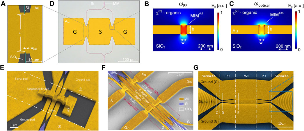
FIGURE 1. Colorized SEM images (A) of a plasmonic phase modulator. Magnitude of the RF (B) and optical (C) Ex field component in the cross section of the metal slot [from (Melikyan et al., 2014)]. (D) Colorized microscope pictures of silicon-plasmonic organic hybrid Mach-Zehnder modulator, where feeding waveguides and MMIs are realized in silicon. Plasmonic phase modulators are visible in both interferometer arms [from (Heni et al., 2015)]. (E) “All-plasmonic” MZM where also the splitting and combining functions are embedded in the plasmonic structure [from (Haffner et al., 2015b)]; (F) similar concept extended to an IO modulator [from (Haffner et al., 2015a)]. (G) Plasmonic MZM structure where grating couplers (GC), polarization rotators (PR) and interferometer (MZI) are realized in a single metal layer [from (Ayata et al., 2017)].
For THz applications, the modulator bandwidth should be sufficiently large to operate over hundreds of GHz. This is possible thanks to the quasi-instantaneous nature of Pockels effect and the extremely small RC time constant of the structure. The small slot height (∼100–150 nm) and short length (in the order of 10 μm) of the plasmonic waveguides allow to keep capacitances within the femtofarad range, while resistances are also very low thanks to the high conductivity of the metal electrodes. This yields a theoretical cutoff frequency in the THz range. Another unique advantage is the device’s compactness, which has recently allowed monolithic integration on electronic integrated circuit platforms, while keeping a low footprint and cost (Koch et al., 2019; Koch et al., 2020; Moor et al., 2022).
2.2 Plasmonic Mach-Zehnder modulator
POH phase modulators can be employed for intensity modulation by arranging them in a photonic Mach-Zehnder interferometer structure, as shown by Heni et al. (2016a), Figure 1D (Heni et al., 2015; Hoessbacher et al., 2016). The modulator is driven in a push-pull configuration by means of a ground-signal-ground (G-S-G) RF probe as indicated by the labels in Figure 1D. Plasmonic IQ modulators with 100 Gbaud capability were also reported (Heni et al., 2018).
2.3 Reducing the size
In the structures described above, most of the chip footprint is occupied by the photonic routing to and from the active plasmonic phase modulator sections. In an effort to reduce footprint even further, all-plasmonic modulators have been realized where also the splitting and combining functions needed for Mach-Zehnder operation are embedded in the plasmonic structure. Haffner et al. (2015b) have shown a Mach-Zehnder modulator (MZM) with a footprint of only 10 µm with insertion losses of 8.1 dB tested at 72 Gbaud symbol rates. Suspended metallic bridges enabled electrical connections within the plasmonic structure, Figure 1E. The same concept was later extended to a full IQ modulator (Haffner et al., 2015a), Figure 1F. Ayata et al. (2017) demonstrated an all-metal structure without any photonic waveguides, where grating couplers, polarization rotators, and Mach-Zehnder region are realized on a single metal layer, Figure 1G.
2.4 Characterizing the speed
The low RC constant of plasmonic structures promises cutoff frequencies in the THz range. Actual measurements of maximum speed of plasmonic modulator devices have been mostly limited by available measurement instrumentation. In an effort to experimentally assess the 3 dB bandwidth of those devices, laboratory tests were conducted by using electrical driving signals from 75 MHz up to 500 GHz (Burla et al., 2019). In these experiments, a continuous-wave (CW) laser at 1547.5 nm with 0 dBm optical power was fed into a plasmonic MZM. The frequency response to the electrical signals were then determined in two different setups that covered the frequency ranges 15–70 GHz and 200–500 GHz. Subsequently, the optical spectrum of the intensity-modulated carrier at the modulator output was measured using an optical spectrum analyzer (OSA). The amplitude ratio between the fundamental and first side lobe in the spectrum was then used to determine the relative response of the electrical signal onto the optical signal (Alloatti et al., 2011). The frequency response was then normalized with respect to the power of the electrical signal driving the modulator. Results show a flat frequency response up to 500 GHz with a ripple that does not cross the −3 dB line compared to the low-frequency response, Figure 2A.
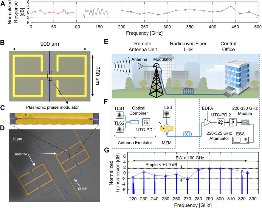
FIGURE 2. (A) Measured response of the plasmonic organic hybrid MZM over the 20–70 GHz and 200–500 GHz range. (B) 60 GHz antenna with integrated plasmonic phase modulator (C). The antenna provides a resonant enhancement of the impinging field up to a factor of approximately 90,000 [from (Salamin et al., 2018)]. (D) Colorized SEM image of the terahertz plasmonic mixer. The silicon (Si) Mach-Zehnder interferometer (MZI) is shown in blue and the antenna coupled plasmonic phase modulator (PPM) in yellow (magnified in the inset) (from [Salamin et al., 2019]). (E) Scenario representing an analog radio-over-fiber link connecting a remote THz antenna to a central office. (F) Experimental setup of the analog link, and (G) measured link gain in the 220–325 GHz range [from (Burla et al., 2019)].
3 Applications to microwave photonics
The broadband characteristics of plasmonic modulators create attractive potential for microwave photonics applications. Here we review two examples of applications to direct sub-THz to optical conversion and analog radio-over-fiber (RoF) links.
3.1 Direct wireless-optical conversion
Converting a THz wireless signal to the optical domain is generally performed in two steps: first, the sub-THz signal is down-converted to baseband, e.g., using a Schottky barrier diode, and then up-converted to the optical domain by electro-optically modulating an optical carrier (Harter et al., 2019; Ummethala et al., 2019). In principle, this double-conversion process could be avoided by directly converting the sub-THz signal to the optical domain. Unfortunately, typical modulators are limited to bandwidths in the order of 100 GHz, rendering the process very inefficient or simply impossible at sub-THz frequencies (Leuthold et al., 2022).
In 2015 a direct RF-to-optical conversion relying on plasmonic modulators was introduced (Salamin et al., 2015). This scheme used a modified plasmonic modulator whose electrodes were shaped into resonant antenna arms, designed to be resonant with the modulator structure and, at the same time, to efficiently collect the impinging electric field, Figure 2B. This provides a built-in field enhancement in the slot compared to the impinging field up to a factor 90,000. Experiments were initially performed at 60 GHz (Salamin et al., 2015); a direct, high-efficiency conversion of sub-THz to optical waves is possible thanks to the inherent resonant field enhancement occurring in the plasmonic slot, visible in Figure 2C. We successfully transmitted 20 and 10 Gbit/s over wireless distances of 1 and 5 m, respectively, at a carrier frequency of 60 GHz (Salamin et al., 2018). More recently the concept has been successfully extended to the 300 GHz band (Salamin et al., 2019), Figure 2D. Additional demonstrations of efficient THz links enabled by plasmonic modulators include a 16 m link carrying 50 Gbit/s at 288.5 GHz (Ummethala et al., 2019). A more recent record demonstration enabled by plasmonic modulators is the transmission of 150 Gbit/s (line-rate) data over a transparent, optical-to-THz-to-optical wireless link operating at a carrier frequency of 228 GHz and a length of 115 m, without using any electrical driver amplifier at the modulator input (Horst et al., 2021; Horst et al., 2022).
3.2 Analog radio-over-fiber links for 6G and beyond
The workhorse of any microwave photonic system is the analog optical link (AOL) or microwave photonic link (MPL) (Cox, 2006; Marpaung et al., 2019). Recently, analog links started to play an increasingly important role in next-generation wireless communications, as they allow to remote mm-wave and sub-THz remote antenna units from central offices without compromising analog bandwidth, Figure 2E. To explore the potential of plasmonics in this field, an analog RoF link was then implemented using a plasmonic modulator similar to Figure 1D. The experimental setup used to emulate the described RoF link scenario is shown in Figure 2F.
Direct THz-to-optical-to-THz conversion was achieved with a flat response over the 220–325 GHz range (>100 GHz bandwidth), only limited by the available electrical test equipment, as visible in Figure 2G. Besides bandwidth and speed, a main figure of merit of analog link is the spurious-free dynamic range (SFDR). This is mainly influenced by the properties of the modulator, in particular losses and non-linearities. Intercept points (Pozar, 2009) of a plasmonic MZM was measured (third order input intercept point, IIP3 = 18.9 dBm) to be on par with those of commercial modulators of equal half-wave voltage optimized for analog applications (IIP3 = 19 dBm). The dynamic range of the link described above was also characterized and displayed an SFDR3 of 105.2 dB/Hz2/3 (Burla et al., 2019).
Phase noise is a critical aspect in any communication link, especially at high frequencies, because it directly impacts the achievable data rate and range. Its value strongly depends on the purity of the optical and electrical signal sources. In this work we do not directly address this aspect, widely discussed in literature (Khayatzadeh et al., 2014), but rather take into account the noise added in the system by the introduction of a photonic link by means of the noise figure parameter (NF). While in our first attempt we had not optimized the sub-THz link, leading to a high, RIN-dominated noise figure above 45 dB (Burla et al., 2019), this value can be reduced by several orders of magnitude by reducing the fiber-to-chip coupling losses and using well-established approaches such as low biasing of the Mach-Zehnder modulator (Marpaung, 2009).
4 Discussion
Plasmonics has proven successful in enabling MWP functions in the THz range, for example, sub-THz analog optical links, direct THz-to-optical conversion by plasmonic mixers and, more recently, high data rate sub-THz wireless links.
Still, one of the main critics to plasmonic modulators is the inherent plasmonic loss of approximately 0.5 dB/μm encountered in the plasmonic waveguide section. High losses are particularly detrimental in analog applications, where RF loss of a link scales as the square of the optical loss in the link (Cox, 2006). Despite that, as described before, thanks to the very high modulation efficiency in these devices, the length of plasmonic waveguide sections can be kept in the 10–20 μm range, thus minimizing the impact of plasmonic losses on the system performance. Furthermore, it should be stressed that losses have been constantly reduced over time. In the recent record demonstration of a 150 Gb/s THz link transmitting information over 150 m, a plasmonic modulator with a low fiber-to-fiber loss of 12 dB was employed. There, approx. 4–5 dB losses were fundamental plasmonic losses; the largest fraction of the losses were attributed to fiber-to-chip coupling (approx. 6–7 dB) and photonic to plasmonic conversion losses (approx. 2 dB). More recently, resonant plasmonic devices with as little as 1.5 dB on-chip losses have emerged, as discussed in the following.
Another important aspect is power consumption. Record-low driving voltage links were reported, e.g., optical links at a bit rate of 120 Gb/s NRZ-OOK below the HD-FEC limit have been demonstrated with only 178 mVpp applied on a dual-drive plasmonic MZM (Baeuerle et al., 2019). In addition to these achievements, new efforts and techniques have been devised to reduce those losses even further, as described below.
4.1 Simultaneous reduction of half-wave voltage and losses
In a MZM, half-wave voltage (Vπ) indicates the voltage required to induce a 180° phase shift between the arms and, in turn, the change from a maximum to a minimum of the modulator transmission function. A low value of this parameter is premium, as it indicates that the modulator can efficiently convert electrical voltage signals to corresponding variations of the optical intensity. Together with insertion loss L, Vπ directly impacts energy consumption per bit in digital links (Heni et al., 2019) and gain in analog optical links, respectively (Ackerman et al., 2016).
Half-wave voltage is linked to the modulator length (and, in turn, to its loss) by the VπL parameter. At first instance, the loss can be reduced by shortening the modulator, and the Vπ can be made smaller mainly by designing a longer modulator. The width of the plasmonic gap also has an effect on Vπ, loss and modulation efficiency, as described in detail in (Haffner et al., 2016b). Several techniques allow to reduce half-wave voltage and loss simultaneously. Besides using electro-optic polymers with higher non-linearity, two approaches have been proven to be particularly effective for the scope.
4.1.1 Leveraging material resonances
The first technique leverages material absorption resonances for reducing losses. It has been shown (Haffner et al., 2017) that the loss of plasmonic modulators can be reduced by a factor 2 and the voltage-length product by a factor 3, by operating the modulators in the vicinity of the material absorption resonances. In fact, when the optical carrier wavelength approaches the material absorption resonance, the electro-optic coefficient r33 (indicating the strength of the material non-linearity) increases by up to a factor 3; at the same time, however, the material losses (even if increased due to resonance) hardly contribute to the overall losses of the plasmonic waveguide. Therefore, operating the modulator near resonances allows an overall increase of r33 while not sensibly increasing the losses. This allows to implement shorter modulators (with as little as half of the loss) while keeping the same half-wave voltage, effectively reducing the VπL.
4.1.2 Structural resonant enhancement
A radically different approach is to explore alternative configurations compared to the Mach-Zehnder one. Low loss and low half-wave voltage can be simultaneously achieved using resonant structures. A demonstration of this was given in (Haffner et al., 2018). It was shown that high plasmonic losses can be bypassed with the concept of “resonant switching.” In this approach, a modulator is realized by using a plasmonic ring resonator structure coupled to a buried low-loss silicon photonic waveguide. Plasmonic waveguide losses can be selectively used or bypassed to achieve intensity modulation with insertion losses as low as 2.5 dB, strong modulation, compact footprint and high speed, simultaneously. Speeds up to 100 GHz have been reported and operation at 72 Gbit/s with voltage swings of 6.6 Vp. Subsequent demonstrations further improved these results by using a silicon photonic racetrack resonator with a plasmonic phase modulator inserted in the racetrack cavity, able to operate at 100 Gbit/s NRZ with a 1.3 Vp (Messner et al., 2020). More recently, OOK line rates of 220 Gbit/s and 408 Gbit/s 8PAM were demonstrated with a similar device, using driver voltages of only 0.6 Vp (Eppenberger et al., 2021), on-chip losses (that is, removing the effect of fiber-to-chip coupling) of only 1.5 dB (Eppenberger et al., 2022), and a measured bandwidth exceeding 110 GHz.
4.2 Future developments
A strong progress is also seen in the stability of operation over time and wide temperature ranges (Heni et al., 2019). Eppenberger et al. have reported stable operation at 80°C for more than 70 min, while the non-linear material itself showed a stable performance at 85°C for over 2000 h with less than 5% variance (Eppenberger et al., 2022).
Other research direction include the use of ferroelectric materials, such as barium titanate (BaTiO3, BTO), which are suitable for wafer-level processing and have proven long-term high-temperature stability (Abel et al., 2019; Messner et al., 2019). This, in turn, enables high optical power handling, which is of high importance in microwave photonics applications.
Plasmonic modulators have shown the capability to be integrated on a single metal layer (Ayata et al., 2017). This opens the possibility to embed them on many different technological platforms. For example, recent demonstrations showed successful integration on silicon nitride (Kohli et al., 2022) with operation up to 216 GBd symbol rates. This is a very versatile photonic technology, offering ultra-low optical losses together with negligible non-linear absorption in the telecom wavelengths. The addition of plasmonic modulators equips this attractive platform with a new key capability, thus opening it to many additional applications and functions that require extremely high speed modulation.
Author contributions
CHo, WH, CHa, and YS designed the plasmonic devices employed in the MWP experiments reviewed in the manuscript. YF, CHo, WH, CHa, and YS fabricated the devices used in the MWP experiments. TW designed grating couplers of the devices used in the MWP experiments. MB conceived, designed and performed the speed characterization, non-linear distortion, dynamic range and analog link experiments. YS conceived, designed and performed the plasmonic mixer experiments. MB and HM performed sub-THz measurements used for the MZM characterization. YH and TB performed the high-speed wireless link experiments. DE and LD provided materials for the devices used in the MWP experiments. MB wrote the first draft of the manuscript. MB and JL wrote sections of the manuscript. JL conceived and supervised the projects. All authors contributed to manuscript revision, read, and approved the submitted version.
Funding
MB acknowledges ERC Grant ELEPHANT (948624) and the SNSF Ambizione Grant 173996. We acknowledge the financial support by the European Commission under the Horizon 2020 project ERC PLASILOR under Grant 670478 and the Horizon 2020 project VERTIGO under Grant 822030. DLE and LRD acknowledge AFOSR grant FA9550-19-1-0069.
Acknowledgments
The authors acknowledge NTT Electronics for the UTC-PD used in the experiments and the Cleanroom Operations Teams of the Binnig and Rohrer Nanotechnology Center (BRNC) for their help and support.
Conflict of interest
CHo and WH are currently employed by Polariton Technologies Inc. CHa is employed by IMEC. DE was employed by NLM Photonics. TW is employed by Soxai Inc. JL acts as Scientific Advisor for Polariton Technologies Inc. Several patents exist in relation to the published research.
The remaining authors declare that the research was conducted in the absence of any commercial or financial relationships that could be construed as a potential conflict of interest.
Publisher’s note
All claims expressed in this article are solely those of the authors and do not necessarily represent those of their affiliated organizations, or those of the publisher, the editors and the reviewers. Any product that may be evaluated in this article, or claim that may be made by its manufacturer, is not guaranteed or endorsed by the publisher.
References
Abel, S., Eltes, F., Ortmann, J. E., Messner, A., Castera, P., Wagner, T., et al. (2019). Large Pockels effect in micro- and nanostructured barium titanate integrated on silicon. Nat. Mater. 18, 42–47. doi:10.1038/s41563-018-0208-0
Ackerman, E. I., Betts, G. E., and Cox, C. H. (2016). Inherently broadband linearized modulator for high-SFDR, low-NF microwave photonic links. 2016 IEEE International Topical Meeting on Microwave Photonics (MWP), Oct. 31 2016-Nov. 3 2016. 265–268.
Akiyama, K., Alberdi, A., Alef, W., Algaba, J. C., Anantua, R., Asada, K., et al. (2022). First Sagittarius A* event Horizon telescope results. I. The shadow of the supermassive black hole in the center of the Milky Way. Astrophysical J. Lett. 930, L12.
Alloatti, L., Korn, D., Palmer, R., Hillerkuss, D., Li, J., Barklund, A., et al. (2011). 42.7 Gbit/s electro-optic modulator in silicon technology. Opt. Express 19, 11841–11851. doi:10.1364/oe.19.011841
Ayata, M., Fedoryshyn, Y., Heni, W., Baeuerle, B., Josten, A., Zahner, M., et al. (2017). High-speed plasmonic modulator in a single metal layer. Science 358, 630–632. doi:10.1126/science.aan5953
Baeuerle, B., Heni, W., Hoessbacher, C., Fedoryshyn, Y., Koch, U., Josten, A., et al. (2019). 120 GBd plasmonic Mach-Zehnder modulator with a novel differential electrode design operated at a peak-to-peak drive voltage of 178 mV. Opt. Express 27, 16823–16832. doi:10.1364/oe.27.016823
Brun, M. A., Formanek, F., Yasuda, A., Sekine, M., Ando, N., and Eishii, Y. (2010). Terahertz imaging applied to cancer diagnosis. Phys. Med. Biol. 55, 4615–4623. doi:10.1088/0031-9155/55/16/001
Burla, M., Hoessbacher, C., Heni, W., Haffner, C., Fedoryshyn, Y., Werner, D., et al. (2019). 500 GHz plasmonic Mach-Zehnder modulator enabling sub-THz microwave photonics. APL Photonics 4, 056106. doi:10.1063/1.5086868
Cai, W., White, J. S., and Brongersma, M. L. (2009). Compact, high-speed and power-efficient electrooptic plasmonic modulators. Nano Lett. 9, 4403–4411. doi:10.1021/nl902701b
Capmany, J., and Novak, D. (2007). Microwave photonics combines two worlds. Nat. Photonics 1, 319–330. doi:10.1038/nphoton.2007.89
Dionne, J. A., Diest, K., Sweatlock, L. A., and Atwater, H. A. (2009). PlasMOStor: A metal− oxide− Si field effect plasmonic modulator. Nano Lett. 9, 897–902. doi:10.1021/nl803868k
Eppenberger, M., Bitachon, B. I., Messner, A., Heni, W., Habegger, P., Destraz, M., et al. Plasmonic racetrack modulator transmitting 220 Gbit/s OOK and 408 Gbit/s 8PAM. 2021 European Conference on Optical Communication (ECOC), 13-16 Sept. 2021 2021. 1–4.
Eppenberger, M., Bitachon, B. I., Messner, A., Heni, W., Moor, D., Kulmer, L., et al. (2022). “Enhanced stability of resonant racetrack plasmonic-organic-hybrid modulators,” in Optical Fiber Communication Conference (OFC) 2022, San Diego, California, 2022/03/06. Editors S. Matsuo, D. Plant, J. Shan Wey, C. Fludger, R. Ryf, and D. Simeonidou (Washington, DC: Optica Publishing Group). doi:10.1364/OFC.2022.Th3C.3
Haffner, C., Chelladurai, D., Fedoryshyn, Y., Josten, A., Baeuerle, B., Heni, W., et al. (2018). Low-loss plasmon-assisted electro-optic modulator. Nature 556, 483–486. doi:10.1038/s41586-018-0031-4
Haffner, C., Heni, W., Elder, D. L., Fedoryshyn, Y., Đorđević, N., Chelladurai, D., et al. (2017). Harnessing nonlinearities near material absorption resonances for reducing losses in plasmonic modulators. Opt. Mater. Express 7, 2168–2181. doi:10.1364/ome.7.002168
Haffner, C., Heni, W., Fedoryshyn, Y., Baeuerle, B., Josten, A., Salamin, Y., et al. Ultra-compact plasmonic IQ-modulator. Optical Communication (ECOC), 2015 European Conference on, Sept. 27 2015-Oct. 1 2015 2015a. 1–3.
Haffner, C., Heni, W., Fedoryshyn, Y., Josten, A., Baeuerle, B., Hoessbacher, C., et al. (2016a). IEEE, 1–18.Plasmonic organic hybrid modulators—scaling highest speed photonics to the microscaleProceedings of the IEEE
Haffner, C., Heni, W., Fedoryshyn, Y., Josten, A., Baeuerle, B., Hössbacher, C., et al. (2016b). Plasmonic organic hybrid modulators - scaling highest speed photonics to the microscale. Proc. IEEE 104, 2362–2379. doi:10.1109/jproc.2016.2547990
Haffner, C., Heni, W., Fedoryshyn, Y., Niegemann, J., Melikyan, A., Elder, D. L., et al. (2015b). All-plasmonic Mach–Zehnder modulator enabling optical high-speed communication at the microscale. Nat. Photonics 9, 525–528. doi:10.1038/nphoton.2015.127
Harter, T., Ummethala, S., Blaicher, M., Muehlbrandt, S., Wolf, S., Weber, M., et al. (2019). Wireless THz link with optoelectronic transmitter and receiver. Optica 6, 1063. doi:10.1364/optica.6.001063
Hecht, J. (2016). The bandwidth bottleneck that is throttling the Internet. Nature 536, 139–142. doi:10.1038/536139a
Heni, W., Baeuerle, B., Fedoryshyn, Y., Josten, A., Haffner, C., Watanabe, T., et al. (2018). “100 GBd plasmonic IQ modulator,” in Conference on Lasers and Electro-Optics, San Jose, California, 2018/05/13. Editors S. Matsuo, D. Plant, J. Shan Wey, C. Fludger, R. Ryf, and D. Simeonidou (Washington, DC: Optical Society of America). doi:10.1364/OFC.2022.Th3C.3
Heni, W., Fedoryshyn, Y., Baeuerle, B., Josten, A., Hoessbacher, C. B., Messner, A., et al. (2019). Plasmonic IQ modulators with attojoule per bit electrical energy consumption. Nat. Commun. 10, 1694. doi:10.1038/s41467-019-09724-7
Heni, W., Haffner, C., Baeuerle, B., Fedoryshyn, Y. M., Josten, A., Hillerkuss, D., et al. (2016a). 108 Gbit/s plasmonic mach-zehnder modulator with > 70-GHz electrical bandwidth. J. Light. Technol. 34, 393–400. doi:10.1109/jlt.2015.2487560
Heni, W., Haffner, C., Johnston, P. V., Elder, D. L., Fedoryshyn, Y., Cottier, R., et al. (2016b). Optimizing plasmonic modulators for in-device nonlinearities of up to 275 pm/V, ITu1A. 1. Washington, DC: Optical Society of America. Integrated Photonics Research, Silicon and Nanophotonics. doi:10.1364/iprsn.2016.itu1a.1
Heni, W., Hoessbacher, C., Haffner, C., Fedoryshyn, Y., Baeuerle, B., Josten, A., et al. (2015). High speed plasmonic modulator array enabling dense optical interconnect solutions. Opt. Express 23, 29746–29757. doi:10.1364/oe.23.029746
Hoessbacher, C., Salamin, Y., Fedoryshyn, Y., Heni, W., Josten, A., Baeuerle, B., et al. (2016). “Optical interconnect with densely integrated plasmonic modulator and germanium photodetector arrays,”. Anaheim in Optical Fiber Communication Conference, 2016/03/20, California (Washington, DC: Optical Society of America). Th1F.6.
Horst, Y., Blatter, T., Kulmer, L., Bitachon, B. I., Baeuerle, B., Destraz, M., et al. (2021). “Transparent optical-THz-optical link transmission over 5/115 m at 240/190 Gbit/s enabled by plasmonics,” in Optical Fiber Communication Conference (OFC) 2021, Washington, DC (Washington, DC: Optical Society of America). F3C.1.
Horst, Y., Blatter, T., Kulmer, L., Bitachon, B. I., Baeuerle, B., Destraz, M., et al. (2022). Transparent optical-THz-optical link at 240/192 Gbit/s over 5/115 m enabled by plasmonics. J. Light. Technol. 40, 1690–1697. doi:10.1109/jlt.2022.3148534
Jin, W., Johnston, P. V., Elder, D. L., Manner, K. T., Garrett, K. E., Kaminsky, W., et al. (2016). Structure-function relationship exploration for enhanced thermal stability and electro-optic activity in monolithic organic NLO chromophores. J. Mater. Chem. C 4, 3119–3124. doi:10.1039/c6tc00358c
Khayatzadeh, R., Poette, J., and Cabon, B. (2014). Impact of phase noise in 60-GHz radio-over-fiber communication system based on passively mode-locked laser. J. Light. Technol. 32, 3529–3535. doi:10.1109/jlt.2014.2322254
Koch, U., Messner, A., Hoessbacher, C., Heni, W., Josten, A., Baeuerle, B., et al. (2019). Ultra-compact terabit plasmonic modulator array. J. Light. Technol. 37, 1484–1491. doi:10.1109/jlt.2019.2899372
Koch, U., Uhl, C., Hettrich, H., Fedoryshyn, Y., Hoessbacher, C., Heni, W., et al. (2020). A monolithic bipolar CMOS electronic–plasmonic high-speed transmitter. Nat. Electron. 3, 338–345. doi:10.1038/s41928-020-0417-9
Kohli, M., Chelladurai, D., Messner, A., Horst, Y., Moor, D., Winiger, J., et al. (2022). “216 GBd plasmonic ferroelectric modulator monolithically integrated on silicon nitride,” in European Conference on Optical Communication (ECOC) 2022, Basel, 2022/09/18. Editors J. Leuthold, C. Harder, B. Offrein, and H. Limberger (Washington, DC: Optica Publishing Group). Tu4E.5.
Leuthold, J., Hoessbacher, C., Muehlbrandt, S., Melikyan, A., Kohl, M., Koos, C., et al. (2013). Plasmonic communications: Light on a wire. Opt. Photonics News 24, 28–35. doi:10.1364/opn.24.5.000028
Leuthold, J., Horst, Y., Blatter, T., Kulmer, L., Ch, L., X00E, R. I. X., et al. (2022). “Plasmonics in future radio communications: Potential and challenges,” in 2022 3rd URSI Atlantic and Asia Pacific Radio Science Meeting (AT-AP-RASC), 30 May-4 June 2022, 1–4.
Marpaung, D. A. I. (2009). High dynamic range analog photonic links: Design and implementation, enschede. Netherlands: Twente University Press (TUP).
Marpaung, D., Yao, J., and Capmany, J. (2019). Integrated microwave photonics. Nat. Photonics 13, 80–90. doi:10.1038/s41566-018-0310-5
Melikyan, A., Alloatti, L., Muslija, A., Hillerkuss, D., Schindler, P. C., Li, J., et al. (2014). High-speed plasmonic phase modulators. Nat. Photonics 8, 229–233. doi:10.1038/nphoton.2014.9
Melikyan, A., Vallaitis, T., Lindenmann, N., Schimmel, T., Freude, W., and Leuthold, J. (2010). A surface plasmon polariton absorption modulator. Opt. Express 19 (9), 8855–8869. doi:10.1364/OE.19.008855
Mercante, A. J., Shi, S., Yao, P., Xie, L., Weikle, R. M., and Prather, D. W. (2018). Thin film lithium niobate electro-optic modulator with terahertz operating bandwidth. Opt. Express 26, 14810–14816. doi:10.1364/oe.26.014810
Messner, A., Baeuerle, B., Heni, W., Leo, E. D., Winiger, J., Habegger, P., et al. (2020). “100 Gbit/s NRZ data modulation in plasmonic racetrack modulators on the silicon photonic platform,” in 2020 European Conference on Optical Communications (ECOC), 6-10 Dec. 2020, 1–3.
Messner, A., Eltes, F., Ma, P., Abel, S., Baeuerle, B., Josten, A., et al. (2019). Plasmonic ferroelectric modulators. J. Light. Technol. 37, 281–290. doi:10.1109/jlt.2018.2881332
Mittleman, D. M. (2013). Frontiers in terahertz sources and plasmonics. Nat. Photonics 7, 666–669. doi:10.1038/nphoton.2013.235
Moor, D., Fedoryshyn, Y., Langenhagen, H., Müllrich, J., Schmid, R., Uhl, C., et al. (2022). “180 GBd electronic-plasmonic IC transmitter,” in Optical Fiber Communication Conference (OFC) 2022, San Diego, California. Editors S. Matsuo, D. Plant, J. Shan Wey, C. Fludger, R. Ryf, and D. Simeonidou (Washington, DC: Optica Publishing Group). M2D.2022/03/063. doi:10.1364/OFC.2022.M2D.3
Nagatsuma, T., Ducournau, G., and Renaud, C. (2016). Advances in terahertz communications accelerated by photonics. Nat. Photonics 10, 371–379. doi:10.1038/nphoton.2016.65
Nikolajsen, T., Leosson, K., and Bozhevolnyi, S. I. (2004). Surface plasmon polariton based modulators and switches operating at telecom wavelengths. Appl. Phys. Lett. 85, 5833–5835. doi:10.1063/1.1835997
Oxenløwe, L. K., Jia, S., Pang, X., Ozolins, O., Yu, X., Hu, H., et al. (2018). “100s gigabit/s THz communication,” in Conference on Lasers and Electro-Optics, San Jose, California, 2018/05/13 (Washington, DC: Optical Society of America). doi:10.1364/CLEO_SI.2018.STu3D.1
Palka, N., Kowalski, M., Ryniec, R., Szustakowski, M., and Czerwińska, E. (2014). “THz screening for civil and military security,” in THz and security applications, 2014//. Editors C. CORSI, and F. SIZOV (Dordrecht: Springer Netherlands), 211–228.
Randhawa, S., Lachèze, S., Renger, J., Bouhelier, A., De Lamaestre, R. E., Dereux, A., et al. (2012). Performance of electro-optical plasmonic ring resonators at telecom wavelengths. Opt. express 20, 2354–2362. doi:10.1364/oe.20.002354
Ren, A., Zahid, A., Fan, D., Yang, X., Imran, M. A., Alomainy, A., et al. (2019). State-of-the-art in terahertz sensing for food and water security – a comprehensive review. Trends Food Sci. Technol. 85, 241–251. doi:10.1016/j.tifs.2019.01.019
Salamin, Y., Baeuerle, B., Heni, W., Abrecht, F. C., Josten, A., Fedoryshyn, Y., et al. (2018). Microwave plasmonic mixer in a transparent fibre–wireless link. Nat. Photonics 12, 749–753. doi:10.1038/s41566-018-0281-6
Salamin, Y., Blatter, T., Horst, Y., Fedoryshyn, Y., Heni, W., Benea-Chelmus, I., et al. (2019). “300 GHz plasmonic mixer,” in 2019 International Topical Meeting on Microwave Photonics (MWP), 7-10 Oct. 2019, 1–4.
Salamin, Y., Heni, W., Haffner, C., Fedoryshyn, Y., Hoessbacher, C., Bonjour, R., et al. (2015). Direct conversion of free space millimeter waves to optical domain by plasmonic modulator antenna. Nano Lett. 15, 8342–8346. doi:10.1021/acs.nanolett.5b04025
Schildkraut, J. S. (1988). Long-range surface plasmon electrooptic modulator. Appl. Opt. 27, 4587–4590. doi:10.1364/ao.27.004587
Seeds, A. J., Shams, H., Fice, M. J., and Renaud, C. C. (2015a). TeraHertz photonics for wireless communications. J. Light. Technol. 33, 579–587. doi:10.1109/jlt.2014.2355137
Seeds, A. J., Shams, H., Fice, M. J., and Renaud, C. C. (2015b). TeraHertz photonics for wireless communications. Light. Technol. J.33, 579–587. doi:10.1109/jlt.2014.2355137
Sengupta, K., Nagatsuma, T., and Mittleman, D. M. (2018). Terahertz integrated electronic and hybrid electronic–photonic systems. Nat. Electron. 1, 622–635. doi:10.1038/s41928-018-0173-2
Shahramian, S., Holyoak, M., Singh, A., Farahani, B. J., and Baeyens, Y. (2018). A fully integrated scalable W-band phased-array module with integrated antennas, self-alignment and self-test. 2018 IEEE International Solid-State Circuits Conference, 11-15 Feb. 2018. 74–76.
Ummethala, S., Harter, T., Koehnle, K., Li, Z., Muehlbrandt, S., Kutuvantavida, Y., et al. (2019). THz-to-optical conversion in wireless communications using an ultra-broadband plasmonic modulator. Nat. Photonics 13, 519–524. doi:10.1038/s41566-019-0475-6
Wang, C., Zhang, M., Chen, X., Bertrand, M., Shams-Ansari, A., Chandrasekhar, S., et al. (2018). Integrated lithium niobate electro-optic modulators operating at CMOS-compatible voltages. Nature 562, 101–104. doi:10.1038/s41586-018-0551-y
Wang, N., Cakmakyapan, S., Lin, Y.-J., Javadi, H., and Jarrahi, M. (2019). Room-temperature heterodyne terahertz detection with quantum-level sensitivity. Nat. Astron. 3, 977–982. doi:10.1038/s41550-019-0828-6
Weigel, P. O., Zhao, J., Fang, K., Al-Rubaye, H., Trotter, D., Hood, D., et al. (2018). Bonded thin film lithium niobate modulator on a silicon photonics platform exceeding 100 GHz 3-dB electrical modulation bandwidth. Opt. Express 26, 23728–23739. doi:10.1364/oe.26.023728
Keywords: microwave photonics, plasmonics, modulators, terahertz, analog links, wireless communications
Citation: Burla M, Hoessbacher C, Heni W, Haffner C, Salamin Y, Fedoryshyn Y, Watanabe T, Massler H, Blatter T, Horst Y, Elder DL, Dalton LR and Leuthold J (2023) Plasmonics for microwave photonics in the THz range. Front. Photonics 4:1067916. doi: 10.3389/fphot.2023.1067916
Received: 12 October 2022; Accepted: 07 March 2023;
Published: 13 April 2023.
Edited by:
Marco Peccianti, Loughborough University, United KingdomReviewed by:
Guillaume Ducournau, Université de Lille, FranceCopyright © 2023 Burla, Hoessbacher, Heni, Haffner, Salamin, Fedoryshyn, Watanabe, Massler, Blatter, Horst, Elder, Dalton and Leuthold. This is an open-access article distributed under the terms of the Creative Commons Attribution License (CC BY). The use, distribution or reproduction in other forums is permitted, provided the original author(s) and the copyright owner(s) are credited and that the original publication in this journal is cited, in accordance with accepted academic practice. No use, distribution or reproduction is permitted which does not comply with these terms.
*Correspondence: Maurizio Burla, YnVybGFAdHUtYmVybGluLmRl; Juerg Leuthold, bGV1dGhvbGRAZXRoei5jaA==