 Ayushi Chauhan
 Rajesh Sharma
 Manjot Singh
 Reena Sharma
- 1Department of Physics, University Institute of Sciences, Chandigarh University, Mohali, Punjab, India
- 2Department of Pure and Applied Physics, Guru Ghasidas Vishwavidyalaya (A Central University), Bilaspur, Chhattisgarh, India
- 3Department of Physics, Rayat Bahra University, Mohali, Punjab, India
- 4Department of Physics, Indian Institute of Technology Ropar, Punjab, India
Optical non-linearities play a crucial role in enabling efficient and ultrafast switching applications that are essential for next-generation photonic devices. ZnS phosphor material produces the best results in terms of increased luminescence quantum yield when doped with certain impurities. Nevertheless, the investigation of the third-order non-linear optical susceptibility of the phosphor materials can be exploited for various switching applications. In this regard, we review the recent advancements in the investigation of non-linear optical properties of ZnS phosphors, where the knowledge of absorption and refraction is utilized in various optical and detector applications. Furthermore, the review highlights strategies employed to enhance the non-linear optical response of phosphor materials as well as a general discussion of an attosecond optical switching scheme which can be used to fabricate devices with petahertz speeds. Consequently, we provide a solution to the unsolved problem of the significant extension of optical limiting applications to switching applications by developing design strategies to manipulate conventional ZnS phosphor material. The potential challenges and future prospects of utilizing phosphor materials for switching applications are also addressed. The strategies for manipulating ZnS phosphor can be generalized for a broad range of other materials by minimizing linear and non-linear losses, while enhancing the values of the non-linear refractive index coefficient. We propose that the figure-of-merit of ZnS material can be enhanced by using a suitable combination of pump and probe wavelength values, which can be useful for optical switching applications.
1 Introduction
The use of phosphor materials has revolutionized scientific and industrial research due to their many applications in light-emitting diodes, optoelectronics, and television displays. Researchers have made numerous efforts to increase the photoluminescence quantum yield of phosphors by using various dopants and quantum confinement techniques. It has been suggested that the photoluminescence quantum yield of phosphors increases in the case of confined structures compared to their bulk counterparts (Sharma and Bhatti, 2007; Nag et al., 2008; Yang et al., 2008; Sharma et al., 2009a; Sharma et al., 2009b; Sharma et al., 2020). However, research in the field of luminescence-based applications of phosphor materials has already reached a satisfactory level; the idea of exploring non-linear properties and their applications is still unclear in the scientific community.
ZnS phosphor falls into the category of materials that are intensively investigated by researchers for various optoelectronics-based applications (Furdyna and Kossut, 1988; Borse et al., 1999; Norris et al., 2001; Luo et al., 2002; Pradhan et al., 2007; Pradhan and Peng, 2007; Thakar et al., 2007; Srivastava et al., 2010). For example, the UV-visible spectra of cobalt doped ZnS nanowires have shown a red shift in comparison to the spectra of pristine ZnS nanowires (Gawai et al., 2016). The photoluminescence quantum yield of cobalt doped ZnS nanoparticles is reduced because the Co-dopant creates the quencher sites in the energy band gap of the host material (Sharma and Bhatti, 2007). Photocatalytic efficiency of ZnS nanocomposites is found to be 84.49% within 180 min for a mixed sample (Dake et al., 2022). As far as the applications are concerned, the nanoparticles have shown inorganic antimicrobial agent properties which can be fabricated by co-precipitation method (Mote et al., 2015). However, there is a limited number of research reports where non-linear characteristics are investigated from an application point of view. The question of whether a good phosphor material can also be a suitable candidate for non-linear optical investigations and applications remains unanswered in the scientific community. Non-degenerate two-photon absorption was explored in a zinc blende-type ZnS single crystal by using the ultrafast pump–probe technique (Chen et al., 2013). The results of two-photon fluorescence spectroscopy and the pump–probe method for ZnS were compared using a white-light continuum as a probe beam to produce a non-degenerate two-photon absorption spectrum (Negres et al., 2002a). A correction to the two-photon absorption cross-section was proposed to account for the chirp and temporal walk-off of the laser pulses. The cross-correlation signals of ZnS were measured at probe wavelengths of 480 nm, 532 nm, and 580 nm, with the pump beam energy and beam width kept at 5 μJ and 500 μm (HW1/e2M), respectively. Semiconductor quantum dots are suitable for photonic switching applications, although the signal-to-noise ratio of photonic switches and the limited number of photons are some of the problems associated with effective implementation from an application point of view (Smith, 1984; Negres et al., 2002b; Wada, 2004; Dorren et al., 2011; Jiang et al., 2020). Optical power consumption and small cross section of the gain medium are the major issues in the development of the logic devices (Jin and Wada, 2014). The pump-probe measurements of ZnS sample are carried out by using pump and probe beam wavelengths at 800 nm and 400 nm, respectively. It has been suggested that swapping the wavelengths of the pump and probe beams in non-degenerate pump-probe measurements can provide additional information about the relaxation time of hot electrons in the conduction band. This can be explained based on group velocity dispersion, where the 800 nm laser beam travels faster than the 400 nm laser beam due to differences in the refractive index values. Therefore, the pump and probe laser beams cannot be at zero delay, as predicted by cross-correlation measurements (Chen et al., 2013).
The electronic and structural properties of short-lived excited states in molecules and semiconductors can be investigated with the help of transient absorption spectroscopy. These measurements are sensitive to the emission wavelength, intensity, and temperature. Transient absorption spectroscopy and stimulated emission depletion fluorescence of molecules can be combined to measure energy state perturbations of interfaces at a nanometer scale (Maly et al., 2017). On the other hand, the pump-probe technique can also be used to investigate the excited state of semiconductors, where the transmission change in the probe beam is measured as a function of the time delay. One advantage of pump-probe spectroscopy over time-resolved fluorescence is that, in the absence of an excited state, only the fluorescence signal remains, providing valuable information about photon absorption in molecules.
The present article is organized as follows: Section 2 is devoted to pump-probe measurements of ZnS phosphor samples and a discussion of the temporal walk-off of pulses in the sample. In this section, we will address the issue of chirp and temporal walk-off of the laser pulses if a white-light continuum is used as a probe beam. In Section 3, various challenges are highlighted for practical photonic switching applications using semiconductor quantum dots. In Section 4, the pump-probe measurements of the ZnS sample are investigated using pump-probe beam wavelengths at 800 nm and 400 nm, respectively. Here, we also address the question of whether swapping the wavelengths of the pump and probe beams in non-degenerate pump-probe measurements can be useful to obtain extra information about the relaxation time of hot electrons in the conduction band. The next question is whether the swapping exercise can be utilized to determine the characteristics of ZnS for application in optical switching devices. Section 5 is devoted to finding an answer to the question of whether an all-optical switch is better than other switching devices. The concept of optical transistors and the potential for optical logic circuits to revolutionize information processing are also discussed in this section at length. The question, how to obtain resolution of the order of attoseconds in optical switching scheme, is also discussed in Section 5 which can be used to fabricate devices with petahertz speeds. Section 6 highlights various strategies to enhance the figure-of-merit of semiconductor materials. The section also addresses the issue of whether the strategies for manipulation of ZnS phosphor can be generalized for a broad range of other materials. Section 7 summarizes the major contributions and future challenges in this field.
2 Pump-probe measurements and temporal walk-off
The non-degenerate two-photon absorption of a ZnS single crystal sample is measured using the experimental configuration illustrated in Figure 1A, where the details of various components are highlighted in the caption. The transmission spectra illustrated in Figure 1B show two-photon absorption because the energies of the pump and probe photons are smaller than the energy bandgap of the ZnS material (Huang et al., 1997; Leeb et al., 1999; Yoffe, 2001; Burda et al., 2005; Erwin et al., 2005; Yang et al., 2006; Norris et al., 2008; Corrado et al., 2009). A problem arose with chirp and temporal walk-off of the laser pulses when a white light continuum was used as the probe beam. This issue was resolved by applying a correction to the two-photon absorption cross-section. The cross-correlation signals of ZnS were estimated at probe wavelengths of 480 nm, 532 nm, and 580 nm, with the pump beam energy and beam width being 5 μJ and 500 μm (HW1/e2M), respectively. The transmittance and temporal width of the signal depend on the relative velocity of the incident pulses onto the sample and the value of the non-linear optical susceptibility. It is important to note that the length of interaction of the pump and probe beams is significantly reduced due to the group velocity mismatch and different wavelengths in the white light continuum. This walk-off effect resulted in a decrease in transmittance when the difference between the frequencies of the pump and probe was increased.
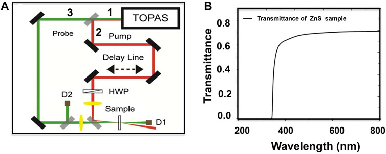
Figure 1. (A) The experimental configuration of pump–probe measurements involves a femtosecond pulsed laser beam (beam 1) from the TOPAS regenerative amplifier, which is split into two parts: beam 2 and beam 3. Beam 2 and beam 3 are respectively named the pump and probe beams. Laser beam 2 is directed onto the sample through an optical delay line and a half-wave plate. Conversely, the laser probe beam 3 is directed onto the sample with the help of a pair of mirrors. A portion of the probe beam is also directed towards detector D2. The pump and probe laser beams are directed onto the ZnS sample, and changes in the probe beam are measured using detector D1. (B) Transmittance spectra of the ZnS single crystal sample (Chen et al., 2013).
The results for the non-degenerate two-photon absorption coefficient (β) in ZnS are represented in Figure 2B, with theoretical estimations included according to Refs Banyai and Koch (1986), Butcher and Cotter (1990), and DeSalvo et al. (1996). The group velocity mismatch (ρ) and non-linearity (τ) parameters of the material corresponding to the wavelengths were 16.4 and 4.5 at 480 nm, 9.9 and 1.9 at 532 nm, and 6.2 and 0.6 at 580 nm, as shown in Figure 2A. This indicates that a significant correction is required to estimate the degenerate and non-degenerate cross-section values when the pump and probe beams have a large separation of frequencies.
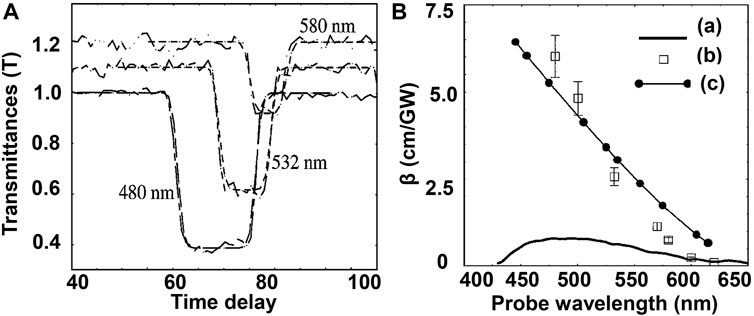
Figure 2. (A) Transmittance as a function of the time delay for a ZnS sample at wavelength of 480, 532 and 580 nm. The experimental results (dashed line) are fitted with solid line curve whose details are referred to the text. (B) Non-degenerate two photon absorption coefficient as a function of probe wavelength for the ZnS sample (a) white light continuum spectral measurement without including pump–probe walk-off. (b) pump–probe walk-off correction is applied (c) calculated spectra of ZnS using theortical model. Reprinted with permission with Negres et al. (2002b) © The Optical Society.
The transmittance can be estimated by fitting the required parameters using following Eq. 1:
Here α, τd, W are the linear absorption coefficient, temporal walk-off parameter, temporal width of the probe and pump pulses, respectively. If n, λ, c are the refractive index at wavelength λ and speed of light, respectively, then the non-linearity can be estimated by following Eq. 2:
Here, L and β are respectively the sample thickness and non-degenerate two-photon absorption coefficient. n and np are the linear refractive indices for the pump and probe beams, respectively. Further, Figure 3 depicits the non-degenerate measurement results where white light continuum probe was used at λp=1.2 μm along with the degenerate two photon absorption spectrum (Garito et al., 1989; Chattopadhyay et al., 2009; Cirloganu et al., 2011; Kumbhakar et al., 2011; Olson et al., 2013). The white light continuum pump-probe technique is beneficial to obtain a database spectra of various organic dyes which can be applied to investigate structure-property relations (Zheng et al., 2017).
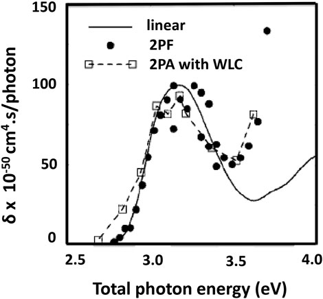
Figure 3. Degenerate two photon absorption cross-section is represented with help of solid circles where two photon fluorescence is taken into account. Non-degenerate cross-section is represented by using open square symbols. Solid line represents the linear absorption spectrum. Reprinted with permission with Negres et al. (2002b)© The Optical Society.
3 Photonic switching applications
Since the reduction in particle size can affect the non-linear properties, semiconductor quantum dots and photonic cavities can be prospective candidates for photonic switching applications. Semiconductor quantum dots are suitable for photonic switching applications, although there are various challenges highlighted in Figure 4. In order to attain a reasonable signal-to-noise ratio in a particular switch for practical applications, the number of incident photons are limited to one thousand (Smith, 1984; Negres et al., 2002b; Wada, 2004; Dorren et al., 2011). On the other hand, the dashed line proposed by Wada in 2004 shows a significant step toward achieving improved performance of photonic switches based on all-optical, electronic, and optoelectronic approaches. In order to develop the practical logic devices, the optical power consumption and the cross-section of the gain medium must be kept small (Jin and Wada, 2014). The requirement for a photonic switch is that it should convert electrical signals to optical signals with a recovery time on the order of picoseconds or femtoseconds. Such photonic switches may have terahertz switching speeds with minimum loss optical waveguides, providing high switching speeds at a low cost.
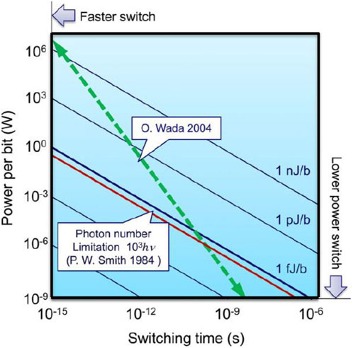
Figure 4. Power per bit as a function of switching time for photonic switches (Smith, 1984).
The results depicted in Figure 5 were recorded by using the experimental configuration Figure 1A where the pump laser beam was fixed at 800 nm while the probe beam wavelength was varied from 480 to 570 nm. When pump and probe laser beams have parallel polarization, the transmission signal was found to be smaller when the probe beam wavelength was increased from 480 nm to 570 nm Figure 5A. This observation was found to similar for the case of orthogonal pump and probe beams (Figure 5B). The non-degenerate two photon absorption coefficients for parallel and orthogonal polarization were estimated by using the concept of crystal orientation and zinc blend symmetry of ZnS single crystals.
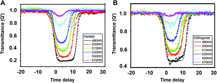
Figure 5. Probe transmission spectra when pump and probe laser beam are in (A) parallel (B) orthogonal polarization mode (Chen et al., 2013). These data are recorded by using the experimental configuration shown in Figure 1A.
The non-degenerate two photon absorption coefficient is estimated to be about 7.52 cm/GW from Figure 6B which is consistent with previous reports of literature (Negres et al., 2002a). It is quite evident from the peak to valley transmission data shown in Figure 6A that there is a large phase change due to the free carrier in comparison to the bound electrons. The value of non-linear refraction coefficient is found to be positive. At zero delay there is a narrow peak for both of the intensity values which can be due to the cascading effect of second-order non-linearities. The carrier recombination time is observed to be 0.6 ns and 0.8 ns for free-carrier absorption and free-carrier refraction, respectively which can be related to the electrons, holes and hole-trapping rates in refraction and absorption. The open aperture z-scan measurements are carried at input beam energies of 10, 30, and 50 mJ which corresponds to the incident intensity values of 0.27, 0.82 and 1.37 GW/cm2, respectively, as shown in Figure 7A. Since the two photon absorption coefficient values do not vary with the increase in the intensity of incident beam (Figure 7B). The non-linear scattering can be estimated by placing a detector at an angle of 45° with respect to the incident beam while recording the scattering signal by translating the sample along the propagation direction of the beam. There is almost no change in the signal which indicate that the non-linear scattering played hardly a role in the non-linear absorption measurements. In order to obtain best options for the material showing optical limiting, the threshold value of incident laser beam intensity and reduction in the transmission play significant role (Wang et al., 1994; Jacobs and Franson, 2009; Christodoulides et al., 2010; Li, 2016; Marder, 2016; Muralidharan et al., 2016). It is quite evident that the luminescence quantum yield can be significantly increased by reduction in the particle size of doped ZnS. Nevertheless, it would be interesting to note whether the reduction of the particle size of the ZnS can also increase the optical limiting behaviour of the material. Since the transmittance of material is decreased with the increased intensity of the incident radiation, the optical limiting effect can be used in various applications where the amount of the light entering a system needs to be controlled. This example put forward a significant point in the mind of scientific community that ZnS can be a candidate for various applications in laser safety devices and protectors from intense radiation.
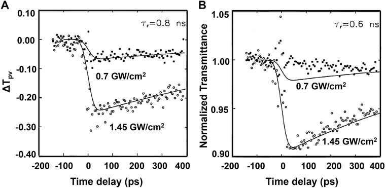
Figure 6. (A) Estimation of non-linear refraction from peak to valley transmission (ΔTpv). (B) Non-linear absorption from the normalized transmittance as a function of probe-beam time delay for ZnS (Sheik-Bahae et al., 1994).
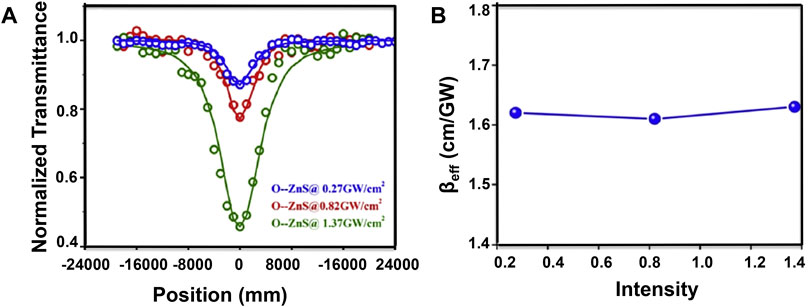
Figure 7. (A) Normalized open aperture z-scan data of ZnS nanocomposites at different intensities (B) absorption coefficient βeff versus intensity I0 with units in (GW/cm2) (Divyasree and Chandrasekharan, 2017).
4 Wavelength swapping and non-linear absorption
Next, the pump-probe measurements of the ZnS sample are conducted using pump-probe beam wavelengths of 800 nm and 400 nm, respectively. Here, we also address the question of whether swapping the wavelengths of the pump and probe beams in non-degenerate pump-probe measurements can provide additional information about the relaxation time of hot electrons in the conduction band. Another question we explore is whether the swapping exercise can be utilized to determine the characteristics of ZnS for application in optical switching devices.
In the first step, the pump and probe beams were kept in a similar polarization state, with wavelength values of 800 nm and 400 nm, respectively. This situation is highlighted in Figure 8A and can be considered as an example of the non-degenerate two-photon absorption process. It is easy to see that there is no transition from subband 1 to subband 2, as three-photon absorption is neglected. On the other hand, one can observe that the linewidth of the pump-probe transmission signal (Figure 8B) is significantly presented in the inset of Figure 8B. This can be explained on the basis of group velocity dispersion, where the 800 nm laser beam travels faster than the 400 nm laser beam due to the difference in the values of refractive indices. Therefore, the pump and probe laser beams cannot be at zero delay, as predicted by the cross-correlation measurements. One can estimate the non-degenerate two-photon absorption coefficient value using the following relation 3:
where, L, npu, npr,
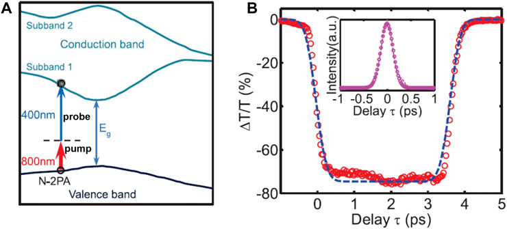
Figure 8. (A) The band structure diagram of non-degenerate two-photon absorption in ZnS where pump and probe laser beams are kept at a wavelength of 800 and 400 nm, respectively. (B) Percentage change in transmission as a function of time delay when probe beam is kept at a wavelength of 400 nm. The inset shows the temporal profile of the fundamental laser beam at a wavelength of 800 nm. The full width at half maximum of the femtosecond laser beam is found to be 200 fs (Wu et al., 2014).
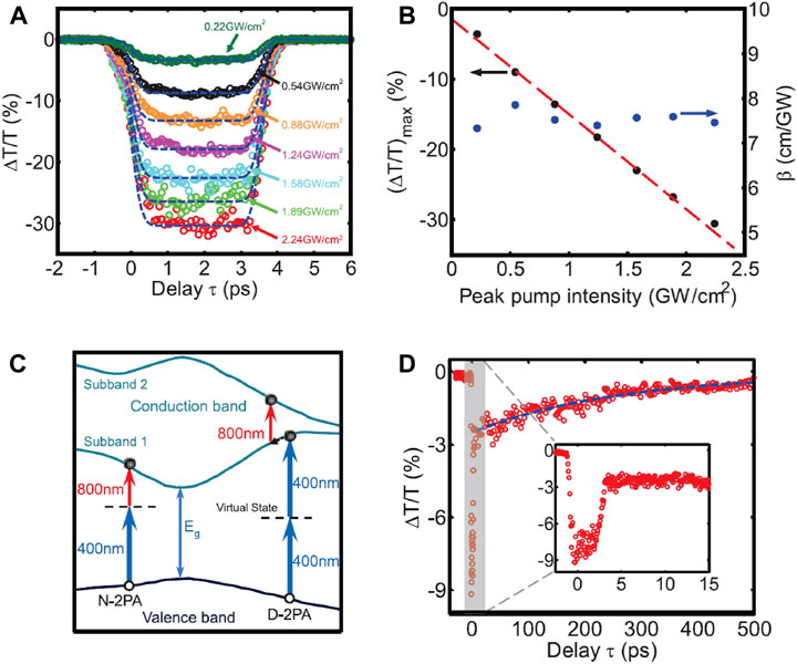
Figure 9. (A) Transmittance change as a function of time delay when the pump and probe beam are kept at wavelength of 800 and 400 nm, respectively. The pump beam intensity is varied from 0.22 to 2.24 GW/cm2. (B) Maximum transmission and non-degenerate two-photon absorption coefficients for various intensities of pump beam. (C) Energy subband structure diagram depciting free carrier absorption, degenerate two photon absorption, non-degenerate two photon absorption processes. (D) The relative transmission as a function of time delay when the pump and probe beams are respectively, kept at 400 and 800 nm wavelength. The inset shows the magnified view of the main level near zero delay (Wu et al., 2014).
The lifetime measurements include a sum of radiative and non-radiative transitions in the materials which can be deconvoluted to extract the various components. Multiexponential decay curves indicate more than one energy state which is responsible for the decay process. On the other hand, single exponential decay means only one state is responsible for decay measurements. Nevertheless, the relaxation processes at a scale of ns and even hundreds of ps can hinder the switch-off state which results in an incomplete switch-off state. In such cases, the switch-on state is sharp enough, however, the switch-off state is not complete, which results in reduced contrast of the switch.
Further studies are required to investigate the effect of the electron-phonon interaction in ZnS. On the other hand, the experimental result in silicon semiconductor shows that the photo-excitation leads to the decrease in the relaxation rates. This can reduce the carrier temperature through the phonon scattering. In order to get the relaxation properties of the hot electrons at relatively higher energy states, the wavelengths of the pump and probe beams are swapped. When the optical delay between the pump and probe is kept around 4 ps, the absorption of the probe photons by hot electrons dominates. We believe that the materials, in which the relaxation time is dominated by the electron-electron and electron-phonon transitions, will be relatively better candidates for switching applications because the carrier scattering occurs at sub-picosecond time scale. On the other hand, if the radiative recombination dominates then it results in the longer lifetime values (ns) of material which produces a long tail and the switch-off state is prolonged over the period of time.
Next, we discuss the question whether the non-linear absorption is affected if the ZnS nanosheet samples are annealed. The situation is highlighted in Figure 10A, where tansmission as a function of Z-position is illustrated for the ZnS nanosheet samples annealed at 400°C for 2 h. The experimental data are fiited by both of the processes; the two photon as well as three-photon absorption. Nevertheless, it is found that the two photon absorption fitting is better than that of the three-photon absorption fitting. This aspect is also validated from the straight line graph of ln(TOA) vs. ln(I), as shown in Figure 10B. There are two important results which can be drawn from the z-scan measurements of the ZnS nanosheet. The two photon absorption is found to be about 10 times higher in ZnS nanocrystal quantum dots as compared to ZnS nanosheet sample which is due to the quantum confinement effect. On the other hand, the two photon absorption coefficient values are also enhanced as a result of annealing of the ZnS nanosheet samples (He et al., 2005; Fishman et al., 2011; Kole et al., 2013; Pattanaik et al., 2013; Shcherbakov et al., 2015; Wu et al., 2019).
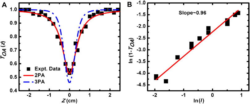
Figure 10. (A) Transmission vs. Z-position of ZnS-ZnO nanocomposite sample in an open aperture z-scan measurements when intensity beam is kept at 2.41 GW/cm2. The symbols represent the experimental data while the two and three photon absorption fittings are shown with the help of solid and dashed lines, respectively (B) time of annealing (TOA) as a function of the intensity (Kole et al., 2014).
The non-linear optical properties of Mn-doped ZnS nanocomposites are investigated to explore the influence of Mn in the host material (El-naggar et al., 2022). Third-order non-linear optical susceptibility and non-linear refractive index values are shown for pure and doped samples of ZnS in Figure 11. It is quite evident that the doped samples have shown smaller values of the non-linear refractive index as compared to the undoped samples of ZnS, which is an opposite trend in the case of the luminescent properties of the host materials, where luminescent properties are enhanced as a result of doping.
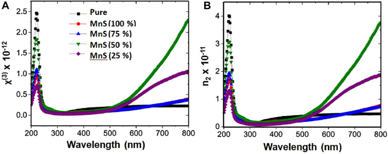
Figure 11. (A) Third-order non-linear optical susceptibility and (B) non-linear refractive index for pure and MnS/ZnS nanocomposites (El-naggar et al., 2022).
The basic principle of the all-optical switching device based on its absorptive nature in the presence of the switching beam is highlighted in Figure 12. The situation is illustrated in Figure 12A, where the input beam is incident on a non-linear optical material, and the output beam is emitted. This state is referred to as the switch-off state of the all-optical switching device. Conversely, when both the input and switching beams are incident on the non-linear material, there is no emission of the output beam, as illustrated in Figure 12B. This state is referred to as the switch-on state of the all-optical switching device. The basic principle of the all-optical switching device based on the change in the direction of the output beam in the presence of the switching beam can also be understood in a similar fashion. Here, the input beam is incident on a non-linear optical material, and the output beam is emitted in a certain direction. This state is referred to as the switch-off state of the all-optical switching device. On the other hand, when both the input and switching beams are incident on the non-linear material, the output beam changes its direction. This state is referred to as the switch-on state of the all-optical switching device based on its directional nature.
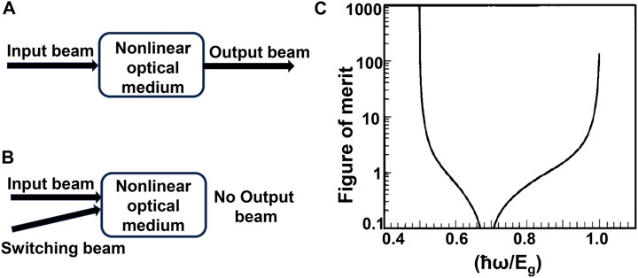
Figure 12. Basic principle of an absorptive all-optical switching device (A) when only input beam is present and (B) when input as well as the switching beams are present. (C) Estimation of figure of merit (Ironside, 1993).
Since the transmittance of material is decreased with the increased intensity of the incident radiation, the optical limiting effect can be used in various applications where the amount of the light entering a system needs to be controlled. In this regard, the two-photon absorption process in ZnS can be useful to extract information whether the material can be a suitable candidate for detector and optical limiting applications. Higher the value of the non-linear absorption coefficient, greater is the possibility of a material to be used in detector and optical limiting applications. Two important points can be noticed from the non-linear absorption coefficient measurements; 1) if a material has high value of non-linear absorption coefficient, then it is not suitable for all-optical switching applications because the figure-of-merit is inversely proportional to the value of non-linear absorption coefficient. 2) Despite a low figure of merit, the material still remains useful for detector and optical limiting applications.
5 Practical applications of all-optical switching devices
The present section is devoted to discuss the challenges for practical applications of an all-optical switch. The concept of optical transistors and the potential for optical logic circuits to revolutionize information processing are also discussed in this section at length. The question, how to obtain resolution of the order of attoseconds in optical switching scheme, is also discussed. The attosecond optical switching scheme can be used to fabricate devices with petahertz speeds which are many orders of magnitude faster than present electronic devices.
To use optical logic for various practical applications, certain conditions must be satisfied, including cascading compatibility, fan-out capabilities, logic-level restoration, input/output isolation, absence of critical biasing, and logic level independence from loss (Miller, 2010). In the case of all-optical switching, cascading compatibility is determined by the spatial and temporal profile of the input and output laser pulses. Nevertheless, feedback stages are important for input and output signals in the case of optical transistors (Miller, 1990; Hwang et al., 2009). Regarding fan-out capabilities, the output of one stage must drive the inputs of about two or more stages in the next step in the transistors. On the other hand, there must be significant transmission even if the input beam power is low. This is in contrast to existing all-optical switching schemes in the literature, where large irradiance values of the input beam are essential to cause non-linear changes in the phase of the output beam. The logic level must be restored while the signal propagates in the medium. In the case of all-optical switching-based schemes, the group velocity dispersion of the pulses must be minimized so that we may get a clean signal after transmission.
Another important parameter is input/output isolation, which can be obtained for the transistors; however, it is difficult in optics because many non-linear processes that occur simultaneously can reduce the final contribution of the signal. In the case of optical signals, the coherent interference of the light beams at different points must be separated, which can justify the absence of critical biasing (Nazarathy et al., 2009). Another challenge is logic level independence from loss in optical switching. It has been observed that the switch-on signals are very clear in the optical switching mechanism; however, the switch-off signals are not as prompt owing to hindrance from various radiative recombination in the semiconductor materials. However, all-optical switching-based devices should have an edge over other switching devices in the future, provided practical implementations are taken into account. It is suggested that the all-optical switching needs further investigation for communication applications.
Most of the findings of researchers in the sub-picosecond all-optical switching domain are in the transmission mode through the target sample, which can attain terabit-rate modulation of the incident signal (Qi et al., 2021; Jiang et al., 2022; Wang et al., 2022; Zhang et al., 2022; Saha et al., 2023; Sun et al., 2023; Wang et al., 2023; Xu et al., 2023). The main challenge with these types of switches lies in the fact that the intensity of the transmitted signal is quite low, while the switch-off state of the device is not as sharp as that of the switch-on state. One particular advantage is that most of these devices in the sub-picosecond switching time domain have been tested for practical applications at the telecommunication wavelength of 1.55 μm.
An example of a recent switch is illustrated in Figure 13A, where the basic principle of an attosecond reflective optical switching device is demonstrated. Reflectivity changes are introduced in the dielectric medium due to the incident pump beam. The pump and probe beams are directed onto the fused silica sample, which is followed by monitoring the reflected probe beam with the help of a photodetector (Figure 13B). The switch-on and switch-off states of the device are shown with attosecond resolution. The attosecond switching as a function of the optical time delay is realized in Figure 13C. The switching signal is shown in Figure 13D when the contribution of the probe beam is subtracted from the overall signal. The switch-on and switch-off states of the attosecond switch are marked with the help of vertical lines using maximum and minimum intensities, respectively. The reflected modulated signal as a function of the optical time delay is shown in Figure 13E. The intensity as a function of wavelength without the pump beam and with the pump beam at zero delay, as well as at an optical delay of 0.9 fs are illustrated in Figure 13F. Therefore, reflectivity-based modulation is demonstrated in the fused silica sample under the influence of a highly intense beam, resulting in attosecond optical switching. Furthermore, this information has been used to obtain a data binary encoding system (Alqattan et al., 2022; Hui et al., 2022; Hui et al., 2023). These original research findings can be used to fabricate devices with petahertz speeds, which are many orders of magnitude faster than present electronic devices.
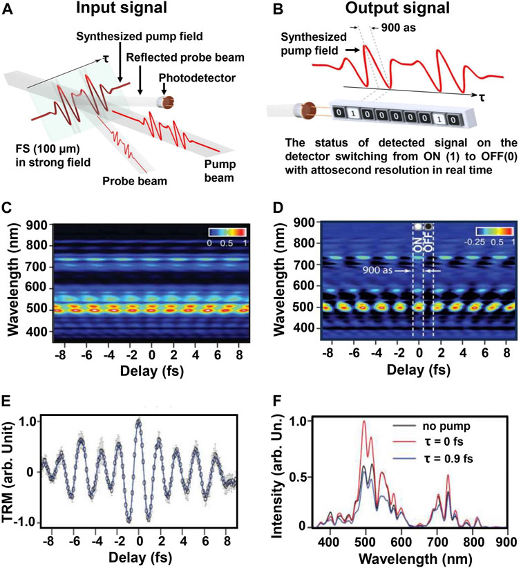
Figure 13. (A) Basic principle of an attosecond reflective optical switching device where pump and probe beams are directed onto a sample of fused silica. (B) The reflected probe beam is monitored with the help of a photodetector. The switch on and switch off states of the device are shown with attosecond resolution. (C) Attosecond optical switching as a function of the time delay. (D) Switching signal when the contribution of the probe beam is subtracted from the overall signal. (E) The reflected modulated signal as a function of the optical time delay. (F) Intensity as a function of wavelength without pump beam and with pump beam at zero delay as well as at 0.9 fs (Hui et al., 2023).
In the visible region, MnS-ZnS (0.5%) not only shows high photocatalytic efficiency (Dake et al., 2022) but also the higher values of non-linear optical parameters which can be useful to obtain fast optical switching in communication systems (Dake et al., 2022). The chalcogenide materials can be used in switching applications where the phase-changes are coupled to the cycling ability and non-volatile nature of the material. In addition, low power consumption and reduced losses are among several other advantages of these materials which demonstrate their potential for future switching applications (Boltasseva and Atwater, 2011; He et al., 2022). On the other hand, ZnS quantum dots can be utilized in various applications in the field of ultrafast photonics and non-linear optics. As an example, in the case of the lasers, the InP/ZnSeS/ZnS quantum dot saturable absorber is used to obtain mode-locked laser pulses with a pulse width of 635 fs. The InP/ZnSeS/ZnS quantum dots fabricated in the presence of hydrogen fluoride can be used to reduce defects which leads to a reduction of the carrier recovery time. The pulse width of the laser is shortened from 635 fs to 450 fs by using InP/ZnSeS/ZnS quantum dots (Lou et al., 2022).
6 Strategies to enhance figure-of-merit
In the photonic devices, the higher power consumption and thermal losses hinder most of the practical applications. All-dielectric meta-materials were investigated for the switching applications because these photonic devices consume less power and the thermal losses are minimal (Boltasseva and Atwater, 2011; Behrens et al., 2019). In this regard, ZnS/SiO2 was considered as one of the material which can be embedded in photonic devices (Li et al., 2011; Wang et al., 2016). These all-dielectric switches can attain picosecond switching speed which can be further increased to femtosecond switching speed with smart selection of the incident beam wavelength and manipulation of the material by doping (Hosokawa et al., 2012; He et al., 2022; Latif et al., 2022; Balaei and Naseri, 2023; Mandal et al., 2023). The linear absorption can be kept low in case of the non-resonant optical non-linearity, therefore, the transmission of light is increased. In case of the non-resonant optical non-linearity, non-linear refractive index, n2, and the non-linear absorption coefficient, α2, values can be related to the Kramers-Kronig relation for a broad range of solids, as illustrated in Figure 6A. It has to be emphasized that the response time of the semiconductor to the incident field is of the order of 10–15 s which can be considered as an instantaneous response.
The schematic evolution of the idea of switching in the present investigations is depicted in Figure 14, where pristine ZnS shows very weak luminescence, which can be considered to originate from defects, band-edge energy states, and excitonic energy levels. The weak emission peak is centered around 420 nm and exhibits luminescence lifetime values of the order of microseconds. This situation is highlighted in Figure 14A. However, luminescence quantum yield is significantly increased when using Mn dopant, owing to the introduction of 4T1 and 6A1 energy states in the host (Figure 14B). The strong luminescence peak is centered around 585 nm, with luminescence lifetime values on the order of milliseconds. Thus, the phosphor nature of ZnS is significantly enhanced by the incorporation of dopants, which can be utilized in various optoelectronic applications. Nevertheless, the situation is drastically altered when the irradiance value of the incident beam on ZnS is high enough to cause non-linear optical effects. Specifically, when the energy bandgap of ZnS is covered with two photons of the same wavelength, the process is called degenerate two-photon absorption, which is used for various optical limiting applications, as illustrated by Figure 14C. Recalling the fact that two-photon absorption contributes to material losses, it is undesirable in the case of switching applications. In the search for schemes to achieve a high figure-of-merit, losses are reduced by using the wavelength of incident radiation where one-photon and two-photon absorption processes are avoided, as shown in Figure 14D. The idea can be extended to a broad range of materials by using the scheme shown in Figure 14E, so that the non-linear refractive index coefficient values are increased. The all-optical switching mechanism in nanocrystal quantum dots is highlighted in Figure 14F, where the spin polarization concept is used.
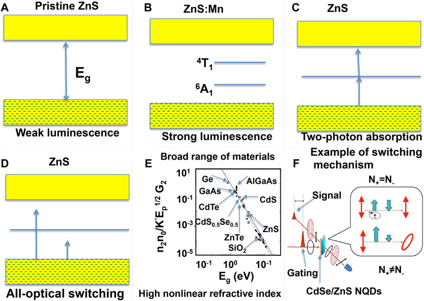
Figure 14. Schematic evolution of the idea of switching in the present investigations: (A) Pristine ZnS has a very low luminescence quantum yield, which can be considered to originate from defects, band-edge energy states, and excitonic energy levels. (B) Luminescence quantum yield is significantly increased when using Mn dopant, owing to the introduction of 4T1 and 6A1 energy states in the host. (C) When the energy bandgap of ZnS is covered with two photons of the same wavelength, the process is called degenerate two-photon absorption, which is used for various optical limiting applications. (D) In the search for schemes to achieve a high figure-of-merit, losses are reduced by using the wavelength of incident radiation where one-photon and two-photon absorption processes are avoided. (E) The idea can be extended to a broad range of materials, increasing the non-linear refractive index coefficient values (Ironside, 1993). (F) The all-optical switching mechanism in nanocrystal quantum dots, where the spin polarization concept is used.
7 Summary
In summary, we have answered the question of whether an all-optical switch is a better candidate than other switching devices. However, all-optical switching-based devices should have an edge over other switching devices in the future, provided practical implementations are taken into account. The concept of optical transistors and the potential for optical logic circuits to revolutionize information processing are also discussed. The pump-probe measurements and temporal walk-off of pulses in the ZnS sample are discussed, addressing the issue of chirp and temporal walk-off of the laser pulses if the white-light continuum is used as the probe beam. Various challenges are elaborated for practical photonic switching applications using semiconductor quantum dots. The pump-probe measurements of the ZnS sample are investigated using pump-probe beam wavelengths at 800 nm and 400 nm, respectively. Here, we have addressed the question of whether swapping the wavelengths of the pump and probe beams in non-degenerate pump-probe measurements can be useful to obtain extra information about the relaxation time of hot electrons in the conduction band. The following question is answered regarding whether the swapping exercise can be utilized to determine the characteristics of ZnS for application in optical switching devices.
In the present paper, we have reviewed the non-linear refraction and absorption mechanism in ZnS phosphors which can be further used to obtain higher figure-of-merit values in order to decide the suitability of materials for the switching applications. The next step will be to extend the present investigations for the study of the non-linear properties of the organic molecules by borrowing the idea from semiconductor materials discussed in the present manuscript. The off-resonant (degenerate), free space optics and Mach–Zehnder interferometer based all-optical switching configurations are already demonstrated by many researchers to test various semiconductor and non-linear organic materials (Sharma et al., 2021). The next challenge is to check the semiconductor and organic materials for realistic applications using a silicon organic hybrid waveguide (Pattanaik et al., 2016). The future road map is to incorporate organic and semiconductor materials in slot waveguide geometry (Sharma et al., 2021). It is to be noted that the figure-of-merit value of about ≥1 is reasonable for the switching applications; however, it is reported that the theoretical estimate of figure-of-merit of the YZ-V-69 organic molecule has attained a value ≥400 (Nalwa, 1993; Marder, 2016). Consequently, these organic materials can be tested for the switching applications by using free space Mach–Zehnder interferometer configuration which can be further extended to design waveguides in the telecommunication sector by embedding the high-figure-of-merit material in the slot wave-guide geometry.
Author contributions
AC: Writing–original draft. RaS: Writing–review and editing, Writing–original draft. MS: Writing–original draft, Investigation, Conceptualization. ReS: Writing–original draft, Validation, Software.
Funding
The authors declare that financial support was received for the research, authorship, and/or publication of this article. The authors acknowledge financial support of Department of Science and Technology, Government of India for Inspire project Grant number IF190054.
Conflict of interest
The authors declare that the research was conducted in the absence of any commercial or financial relationships that could be construed as a potential conflict of interest.
Publisher’s note
All claims expressed in this article are solely those of the authors and do not necessarily represent those of their affiliated organizations, or those of the publisher, the editors, and the reviewers. Any product that may be evaluated in this article, or claim that may be made by its manufacturer, is not guaranteed or endorsed by the publisher.
References
Alqattan, H., Hui, D., Sennary, M., and Hassan, M. T. (2022). Attosecond electronic delay response in dielectric materials. Faraday Discuss. 237, 317–326. doi:10.1039/d2fd00002d
Balaei, M., and Naseri, T. (2023). Efficient and enhanced optical switches based on saturation absorption via composite of 2D materials. Opt. Laser Technol. 161, 109208. doi:10.1016/j.optlastec.2023.109208
Banyai, L., and Koch, S. W. (1986). A simple theory for the effects of the plasma screening on the optical spectra of highly excited semiconductors. Z. Phys. B 63, 283.
Behrens, M., Lotnyk, A., Gerlach, J. W., Ehrhardt, M., Lorenz, P., and Rauschenbach, B. (2019). Direct measurement of crystal growth velocity in epitaxial phase-change material thin films. ACS Appl. Mater. Interfaces 11, 41544–41550. doi:10.1021/acsami.9b16111
Boltasseva, A., and Atwater, H. A. (2011). Low-loss plasmonic metamaterials. Science 331, 290–291. doi:10.1126/science.1198258
Borse, P. H., Srinivas, D., Shinde, R. F., Date, S. K., Vogel, W., and Kulkarni, S. K. (1999). Effect of Mn2+ concentration in ZnS nanoparticles on photoluminescence and electron-spin-resonance spectra. Phys. Rev. B 60 (12), 8659–8664. doi:10.1103/physrevb.60.8659
Burda, C., Chen, X., Narayanan, R., and El-Sayed, M. A. (2005). Chemistry and properties of nanocrystals of different shapes. Chem. Rev. 105 (4), 1025–1102. doi:10.1021/cr030063a
Butcher, P. N., and Cotter, D. (1990) The elements of nonlinear optics. Cambridge: Cambridge U. Press. Chap. 7.
Chattopadhyay, M., Kumbhakar, P., Sarkar, R., and Mitra, A. K. (2009). Enhanced three-photon absorption and nonlinear refraction in ZnS and Mn2+ doped ZnS quantum dots. Appl. Phys. Lett. 95, 163115. doi:10.1063/1.3254186
Chen, S., Zheng, M. L., Dong, X. Z., Zhao, Z. S., and Duan, X. M. (2013). Nondegenerate two-photon absorption in a zinc blende-type ZnS single crystal using the femtosecond pump–probe technique. J. Opt. Soc. Am. B 30 (12), 3117–3122. doi:10.1364/josab.30.003117
Christodoulides, D. N., Khoo, I. C., Salamo, G. J., Stegeman, G. I., and Van Stryland, E. W. (2010). Nonlinear refraction and absorption: mechanisms and magnitudes. Adv. Opt. Photonics 2, 60–200. doi:10.1364/aop.2.000060
Cirloganu, C. M., Padilha, L. A., Fishman, D. A., Webster, S., Hagan, D. J., and Van Stryland, E. W. (2011). Extremely nondegenerate two-photon absorption in direct-gap semiconductors [Invited]. Opt. Express 19, 22951. doi:10.1364/oe.19.022951
Corrado, C., Jiang, Y., Oba, F., Kozina, M., Bridges, F., and Zhang, J. Z. (2009). Synthesis, structural, and optical properties of stable ZnS:Cu, Cl nanocrystals. J. Phys. Chem. A 113, 3830–3839. doi:10.1021/jp809666t
Dake, D. V., Raskar, N. D., Mane, V. A., Sonpir, R. B., Khawal, H. A., Deshpande, U., et al. (2022). Photocatalytic performance of graphene-based Cr-substituted β ZnS nanocomposites. Appl. Phys. A 128 (4), 276. doi:10.1007/s00339-022-05407-1
DeSalvo, R., Said, A. A., Hagan, D. J., Van Stryland, E. W., and Sheik-Bahae, M. (1996). Infrared to ultraviolet measurements of two-photon absorption and n/sub 2/in wide bandgap solids. IEEE J. Quantum Electron. 32, 1324–1333. doi:10.1109/3.511545
Divyasree, M. C., and Chandrasekharan, K. (2017). Structural and nonlinear optical characterizations of ZnS/PVP nanocomposites synthesized by pulsed laser ablation. Opt. Mater. 67, 119–124. doi:10.1016/j.optmat.2016.12.025
Dorren, H. J. S., Duan, P., Raz, O., and Luijten, R. P. (2011). “Fundamental bounds fr photonic interconnects OECC (Kaohsiung, Taiwan),” in 16th Opto-Electronics and Communications Conference, Kaohsiung, Taiwan, 04-08 July 2011.
El-naggar, A. M., Heiba, Z. K., Mohamed, M. B., Kamal, A. M., Lakshminarayana, G., and Abd-Elkader, O. H. (2022). Effect of MnS/ZnS nanocomposite on the structural, linear and nonlinear optical properties of PVA/CMC blended polymer. Opt. Mater. 128, 112379. doi:10.1016/j.optmat.2022.112379
Erwin, S. C., Zu, L., Haftel, M. I., Efros, A. L., Kennedy, T. A., and Norris, D. J. (2005). Doping semiconductor nanocrystals. Nature 436 (7047), 91–94. doi:10.1038/nature03832
Fishman, D. A., Cirloganu, C. M., Webster, S., Padilha, L. A., Monroe, M., Hagan, D. J., et al. (2011). Sensitive mid-infrared detection in wide-bandgap semiconductors using extreme non-degenerate two-photon absorption. Nat. Photonics 5, 561–565. doi:10.1038/nphoton.2011.168
Furdyna, J. K.,, and Kossut, J. (1988). Diluted magnetic semiconductors; semiconductors and semimetals (New York: Academic).
Garito, A. F., Heflin, J. R., Wong, K. Y., and Zamani- Khamiri, O. (1989). in Organic materials for nonlinear optics III. Editors R. Hann, and O. Bloor (London: Royal Society of Chemistry), 16.
Gawai, U. P., Khawal, H. A., Shripathi, T., and Dole, B. N. (2016). A study on the synthesis, pair distribution function and diverse properties of cobalt doped ZnS nanowires. CrystEngComm 18, 1439–1445. doi:10.1039/c5ce02253c
He, J., Qu, Y. L., Li, H. P., Mi, J., and Ji, W. (2005). Three-photon absorption in ZnO and ZnS crystals. Opt. Express 13, 9235. doi:10.1364/opex.13.009235
He, Q., Liu, Z., Lu, Y., Ban, G., Tong, H., Wang, Y., et al. (2022). Low-loss ultrafast and nonvolatile all-optical switch enabled by all-dielectric phase change materials. Iscience 25 (6), 104375. doi:10.1016/j.isci.2022.104375
Hosokawa, S., Pilgrim, W.-C., Ho hle, A., Szubrin, D., Boudet, N., Be rar, J.-F., et al. (2012). Key experimental information on intermediate-range atomic structures in amorphous Ge2Sb2Te5 phase change material. J. Appl. Phys. 111, 083517. doi:10.1063/1.3703570
Huang, J., Yang, Y., Xue, S., Yang, B., Liu, S., and Shen, J. (1997). Photoluminescence and electroluminescence of ZnS:Cu nanocrystals in polymeric networks. Appl. Phys. Lett. 70, 2335–2337. doi:10.1063/1.118866
Hui, D., Alqattan, H., Yamada, S., Pervak, V., Yabana, K., and Hassan, M. T. (2022). Attosecond electron motion control in dielectric. Nat. Phot. 16, 33–37. doi:10.1038/s41566-021-00918-4
Hui, D., Alqattan, H., Zhang, S., Pervak, V., Chowdhury, E., and Hassan, M. T. (2023). Ultrafast optical switching and data encoding on synthesized light fields. Sci. Adv. 9, eadf1015. doi:10.1126/sciadv.adf1015
Hwang, J., Pototschnig, M., Lettow, R., Zumofen, G., Renn, A., Gotzinger, S., et al. (2009). A single-molecule optical transistor. Nature 460, 76–80. doi:10.1038/nature08134
Ironside, C. N. (1993). Ultra-fast all-optical switching. Contemp. Phys. 34 (1), 1–18. doi:10.1080/00107519308211070
Jacobs, B. C., and Franson, J. D. (2009). All-optical switching using the quantum Zeno effect and two-photon absorption. Phys. Rev. A 79, 063830. doi:10.1103/physreva.79.063830
Jiang, H., Zhao, Y., Ma, H., Wu, Yi, Chen, M., Wang, M., et al. (2022). Broad-band ultrafast all-optical switching based on enhanced nonlinear absorption in corrugated indium tin oxide films. ACS Nano 16 (8), 12878–12888. doi:10.1021/acsnano.2c05139
Jiang, T., Yin, K., Wang, C., You, J., Ouyang, H., Miao, R., et al. (2020). Ultrafast fiber lasers mode-locked by two-dimensional materials: review and prospect. Photonics Res. 8, 78. doi:10.1364/prj.8.000078
Jin, C. Y., and Wada, O. (2014). Photonic switching devices based on semiconductor nanostructures. J. Phys. D Appl. Phys. 47 (13), 133001. doi:10.1088/0022-3727/47/13/133001
Kole, A. K., Kumbhakar, P., and Chatterjee, U. (2014). Observations on nonlinear optical properties of ZnS nanosheet, ZnS–ZnO composite nanosheet and porous ZnO nanostructures dispersed in aqueous medium. Chem. Phys. Lett. 591, 93–98. doi:10.1016/j.cplett.2013.11.016
Kole, A. K., Tiwary, C. S., and Kumbhakar, P. (2013). Ethylenediamine assisted synthesis of wurtzite zinc sulphide nanosheets and porous zinc oxide nanostructures: near white light photoluminescence emission and photocatalytic activity under visible light irradiation. CrystEngComm 15, 5515. doi:10.1039/c3ce40531a
Kumbhakar, P., Chattopadhyay, M., Sarkar, R., and Chatterjee, U. (2011). Chin. Opt. Lett. 9, 101902.
Latif, A. A., Asyikin, A. S., Halimah, M. K., Zaid, M. H. M., Kamarudin, M. A., Faznny, M. F., et al. (2022). Structural, linear and nonlinear optical properties of samarium doped tellurite based glasses for potential optical switching application. Available at: https://ssrn.com/abstract=4122171.
Leeb, J., Gebhardt, V., Müller, G., Haarer, D., Su, D., Giersig, M., et al. (1999). Colloidal synthesis and electroluminescence properties of nanoporous Mn II ZnS films. J. Phys. Chem. B 103, 7839–7845. doi:10.1021/jp991514r
Li, C. (2016) Nonlinear optics: principles and applications. first ed. Berlin, Heidelberg: Springer.
Li, X.-B., Liu, X., Liu, X., Han, D., Zhang, Z., Han, X., et al. (2011). Role of electronic excitation in the amorphization of Ge-Sb-Te al loys. Phys. Rev. Lett. 107, 015501. doi:10.1103/physrevlett.107.015501
Lou, Y., He, P., Ge, B., Duan, X., Hu, L., Zhang, X., et al. (2022). InP/ZnSeS/ZnS core–shell quantum dots as novel saturable absorbers in mode-locked fiber lasers. Adv. Opt. Mater. 11, 2201939. doi:10.1002/adom.202201939
Luo, W., Ismail-Beigi, S., Cohen, M. L., and Louie, S. G. (2002). Quasiparticle band structure of ZnS and ZnSe. Phys. Rev. B 66 (19), 195215. doi:10.1103/physrevb.66.195215
Maly, P., Ravensbergen, J., Kennis, J., Van Grondelle, R., Croce, R., Mančal, T., et al. (2017). Polarization-controlled optimal scatter suppression in transient absorption spectroscopy. Sci. Rep. 7 (1), 43484–43487. doi:10.1038/srep43484
Mandal, M., De, P., Lakshan, S., Sarfaraj, M. N., Hazra, S., Dey, A., et al. (2023). A review of electro-optic, semiconductor optical amplifier and photonic crystal-based optical switches for application in quantum computing. J. Opt. 52 (2), 603–611. doi:10.1007/s12596-022-01045-1
Marder, S. R. (2016). Materials for third-order nonlinear optics. MRS Bull. 41, 53–62. doi:10.1557/mrs.2015.310
Miller, D. A. B. (2010). Are optical transistors the logical next step? Nat. Photonics 4, 3–5. doi:10.1038/nphoton.2009.240
Mote, V. D., Purushotham, Y., Shinde, R. S., Salunke, S. D., and Dole, B. N. (2015). Structural, optical and antibacterial properties of yttrium doped ZnO nanoparticles. Ceramica 61, 457–461. doi:10.1590/0366-69132015613601932
Muralidharan, M. N., Mathew, S., Seema, A., Radhakrishnan, P., and Kurian, T. (2016). Optical limiting properties of in situ reduced graphene oxide/polymer nanocomposites. Mater. Chem. Phys. 171, 367–373. doi:10.1016/j.matchemphys.2016.01.030
Nag, A., Chakraborty, S., and Sarma, D. D. (2008). To dope Mn2+ in a semiconducting nanocrystal. J. Am. Chem. Soc. 130 (32), 10605–10611. doi:10.1021/ja801249z
Nalwa, H. S. (1993). Organic Materials for third-order nonlinear optics. Adv. Mater. 5, 341–358. doi:10.1002/adma.19930050504
Nazarathy, M., Zalevsky, Z., Rudnitsky, A., Larom, B., Nevet, A., Orenstein, M., et al. (2009). All-optical linear reconfigurable logic with nonlinear phase erasure. J. Opt. Soc. Am. A 26, A21–A39. doi:10.1364/josaa.26.000a21
Negres, R. A., Hales, J. M., Kobyakov, A., Hagan, D. J., and Van Stryland, E. W. (2002a). Experiment and analysis of two-photon absorption spectroscopy using a white-light continuum probe. IEEE J. Quantum Electron. 38, 1205–1216. doi:10.1109/jqe.2002.802448
Negres, R. A., Hales, J. M., Kobyakov, A., Hagan, D. J., and Van Stryland, E. W. (2002b). Two-photon spectroscopy and analysis with a white-light continuum probe. Opt. Lett. 27 (4), 270–272. doi:10.1364/ol.27.000270
Norris, D. J., Efros, A. L., and Erwin, S. C. (2008). Doped nanocrystals. Science 319 (5871), 1776–1779. doi:10.1126/science.1143802
Norris, D. J., Yao, N., Charnock, F. T., and Kennedy, T. A. (2001). High-quality manganese-doped ZnSe nanocrystals. Nano Lett. 1 (1), 3–7. doi:10.1021/nl005503h
Olson, B. V., Gehlsen, M. P., and Boggess, T. F. (2013). Nondegenerate two-photon absorption in GaSb. Opt. Commun. 304, 54–57. doi:10.1016/j.optcom.2013.04.035
Pattanaik, H. S., Fishman, D. A., Hagan, D. J., and Van Stryland, E. W. (2013). Pulsed and CW IR detection in wide-gap semiconductors using extremely non-degenerate two-photon absorption. Proc. Conf. Lasers Electro-Opt CTu3E3, 1. doi:10.1364/cleo_si.2013.ctu3e.3
Pattanaik, H. S., Reichert, M., Hagan, K. J. B. D. J., and Van Stryland, E. W. (2016). Enhancement of two-photon absorption in quantum wells for extremely nondegenerate photon pairs. J. Quant. Electron IEEE 52, 9000114.
Pradhan, N., Battaglia, D. M., Liu, Y., and Peng, X. (2007). Efficient, stable, small, and water-soluble doped ZnSe nanocrystal emitters as non-cadmium biomedical labels. Nano Lett. 7 (2), 312–317. doi:10.1021/nl062336y
Pradhan, N., and Peng, X. (2007). Efficient and color-tunable Mn-doped ZnSe nanocrystal emitters: control of optical performance via greener synthetic chemistry. J. Am. Chem. Soc. 129 (11), 3339–3347. doi:10.1021/ja068360v
Qi, H., Wang, X., Hu, X., Du, Z., Yang, J., Yu, Z., et al. (2021). All-optical switch based on novel physics effects. J. Appl. Phys. 129, 210906. doi:10.1063/5.0048878
Saha, S., Diroll, B. T., Ozlu, M. G., Chowdhury, S. N., Peana, S., Kudyshev, Z., et al. (2023). Engineering the temporal dynamics of all-optical switching with fast and slow materials. Nat. Commun. 14, 5877. doi:10.1038/s41467-023-41377-5
Sharma, R., and Bhatti, H. S. (2007). Photoluminescence decay kinetics of doped ZnS nano phosphors. Nanotechnology 18 (46), 465703. doi:10.1088/0957-4484/18/46/465703
Sharma, R., Bhatti, H. S., and Kyhm, K. (2009a). Enhanced oscillator strengths and optical parameters of doped ZnS bulk and nano phosphors. Appl. Phys. B 97, 145–155. doi:10.1007/s00340-009-3632-7
Sharma, R., Kim, B. J., Cho, C., and Kyhm, K. (2009b). Modal optical gain and cavity mode analysis of unstructured and optically structured ZnO nanocrystalline thin films. J. Phys. D Appl. Phys. 42, 135421. doi:10.1088/0022-3727/42/13/135421
Sharma, R., Singh, M., and Kaur, H. (2021). Recent advances in high-figure-of-merit semiconductor and organic materials for all-optical switching applications. J. Mat. Sci. 56, 2838–2855. doi:10.1007/s10853-020-05486-6
Sharma, R., Singh, M., and Sharma, R. (2020). Recent advances in STED and RESOLFT super-resolution imaging techniques. Spectrochimica Acta Part A Mol. Biomol. Spectrosc. 231, 117715. doi:10.1016/j.saa.2019.117715
Shcherbakov, M. R., Vabishchevich, P. P., Shorokhov, A. S., Chong, K. E., Choi, D.-Y., Staude, I., et al. (2015). Ultrafast all-optical switching with magnetic resonances in nonlinear dielectric nanostructures. Nano Lett. 15, 6985–6990. doi:10.1021/acs.nanolett.5b02989
Sheik-Bahae, M., Wang, J., and Van Stryland, E. (1994). Nondegenerate optical Kerr effect in semiconductors. IEEE J. Quantum Electron. 30, 249–255. doi:10.1109/3.283767
Smith, P. W. (1984). Application of all-optical switching and logic. Phil. Trans. R. Soc. A 313, 349–355.
Srivastava, B. B., Jana, S., Karan, N. S., Paria, S., Jana, N. R., Sarma, D. D., et al. (2010). Highly luminescent Mn-doped ZnS nanocrystals: gram-scale synthesis. J. Phys. Chem. Lett. 1 (9), 1454–1458. doi:10.1021/jz100378w
Sun, Y., Larin, A., Mozharov, A., Ageev, E., Pashina, O., Komissarenko, F., et al. (2023). All-optical generation of static electric field in a single metal-semiconductor nanoantenna. Light Sci. Appl. 12, 237. doi:10.1038/s41377-023-01262-8
Thakar, R., Chen, Y., and Snee, P. T. (2007). Efficient emission from core/(doped) shell nanoparticles: applications for chemical sensing. Nano Lett. 7 (11), 3429–3432. doi:10.1021/nl0719168
Wada, O. (2004). Femtosecond all-optical devices for ultrafast communication and signal processing. New J. Phys. 6, 183. doi:10.1088/1367-2630/6/1/183
Wang, J., Sheik-Bahae, M., Said, A. A., Hagan, D. J., and Van Stryland, E. W. (1994). Time-resolved Z-scan measurements of optical nonlinearities. J. Opt. Soc. Am. B 11 (6), 1009–1017. doi:10.1364/josab.11.001009
Wang, Q., Rogers, E. T., Gholipour, B., Wang, C.-M., Yuan, G., Teng, J., et al. (2016). Optically reconfigurable metasurfaces and photonic devices based on phase change materials. Nat. Photonics 10, 60–65. doi:10.1038/nphoton.2015.247
Wang, W., Huang, Lu, Zhang, Q., Yuan, X., Ali, M., Meng, Q., et al. (2022). Ultrafast third-order nonlinear optical response of Ag modified ZnSe/ZnS core-shell structure quantum dots composite films. Optik 252, 168537. doi:10.1016/j.ijleo.2021.168537
Wang, Y., Liu, Yu, Jiang, P., Gao, Y., Yang, H., Peng, L.-Y., et al. (2023). Optical switch of electron-hole and electron-electron collisions in semiconductors. Phys. Rev. B 107, L161301. doi:10.1103/physrevb.107.l161301
Wu, L., Dong, Y., Zhao, J., Ma, D., Huang, W., Zhang, Y., et al. (2019). Kerr nonlinearity in 2D graphdiyne for passive photonic diodes. Adv. Mater. 31, 1807981. doi:10.1002/adma.201807981
Wu, Y. E., Ren, M., Wang, Z., Li, W., Wu, Q., Yi, S., et al. (2014). Optical nonlinear dynamics in ZnS from femtosecond laser pulses. AIP Adv. 4 (5). doi:10.1063/1.4876235
Xu, J., Peng, Y., Qian, S., and Jiang, L. (2023). Microstructured all-optical switching based on two-dimensional material. Coatings 13 (5), 876. doi:10.3390/coatings13050876
Yang, Y., Chen, O., Angerhofer, A., and Cao, Y. C. (2006). Radial-position-controlled doping in CdS/ZnS core/shell nanocrystals. J. Am. Chem. Soc. 128 (38), 12428–12429. doi:10.1021/ja064818h
Yang, Y., Chen, O., Angerhofer, A., and Cao, Y. C. (2008). On doping CdS/ZnS core/shell nanocrystals with Mn. J. Am. Chem. Soc. 130 (46), 15649–15661. doi:10.1021/ja805736k
Yoffe, A. D. (2001). Semiconductor quantum dots, and related systems: electronic, optical, luminescence and related properties of low dimensional systems. Adv. Phys. 50 (1), 1–208. doi:10.1080/00018730010006608
Zhang, P., Chung, T. F., Li, Q., Wang, S., Wang, Q., Huey, W. L. B., et al. (2022). All-optical switching of magnetization in atomically thin CrI3. Nat. Mat. 21, 1373–1378. doi:10.1038/s41563-022-01354-7
Keywords: zinc sulphide (ZnS) phosphor, pump-probe measurements, figure-of-merit, all-optical switching, non-linear refractive index, non-linear absorption coefficient, two-photon absorption
Citation: Chauhan A, Sharma R, Singh M and Sharma R (2024) Optical non-linearities and applications of ZnS phosphors. Adv. Opt. Technol. 13:1390474. doi: 10.3389/aot.2024.1390474
Received: 23 February 2024; Accepted: 23 April 2024;
Published: 09 May 2024.
Edited by:
David González-Andrade, UMR9001 Centre de Nanosciences et de Nanotechnologies (C2N), FranceReviewed by:
Babasaheb Dole, Dr. Babasaheb Ambedkar Marathwada University, IndiaGeorgios Ctistis, Institute for Nanophotonics e.V., Germany
Angel Ortega Gomez, Public University of Navarre, Spain
Copyright © 2024 Chauhan, Sharma, Singh and Sharma. This is an open-access article distributed under the terms of the Creative Commons Attribution License (CC BY). The use, distribution or reproduction in other forums is permitted, provided the original author(s) and the copyright owner(s) are credited and that the original publication in this journal is cited, in accordance with accepted academic practice. No use, distribution or reproduction is permitted which does not comply with these terms.
*Correspondence: Rajesh Sharma, c2hhcm1hX3JhamVzaDEyMzRAeWFob28uY29t