 Saunak Bhattacharya
 Abhijit Kundu
 Jhuma Kundu2
 Angsuman Sarkar
- 1Department of Electronics & Communication Engineering, Chaibasa Engineering College, Jharkhand, India
- 2Department of Electronics & Communication Engineering, NSHM Knowledge Campus, Durgapur, West Bengal, India
- 3Department of Electronics & Communication Engineering, Kalyani Govt. Engineering College, Kalyani, India
- 4Department of Physics, Adamas University, Kolkata, India
In this paper, the authors explore the potential of an exotic multi-graphene layer/Si nanowire (MGL/SiNW) pin device as a switch in the THz frequency domain. The device is developed by the incorporation of multiple SiNWs into its intrinsic region. In contrast, cap and bottom layers are developed by the incorporation of multiple graphene layers. The electrical characterization of the proposed exotic pin device is carried out by developing a quantum-rectified Schrodinger–Poisson drift-diffusion (QRSP-DD) model. The developed QRSP-DD model is validated by analyzing experimental and simulation observations under similar operating conditions. After establishing its validity, the same model in conjunction with the PSpice simulator is used to obtain the switching characteristics of MGL/SiNW pin-based series-shunt and shunt single-pole single-throw (SPST), single-pole double-throw (SPDT), and single-pole multiple-throw (SPMT) switches in the THz frequency domain. The analysis proves that the MGL/SiNW pin-based SPMT switch offers low resistance (0.56 Ω), high isolation (91.15 dB), and low insertion loss (0.007 dB) at 5 THz frequency compared to its SiNW counterpart.
1 Introduction
In recent years, device engineers have shown a remarkable increase in research interest in developing high-frequency switches due to their extensive applications in modern communication and defense sectors (Mamedes and Bornemann, 2021; Pratt and Oliver, 2021; Xu et al., 2021; Kundu et al., 2021a; Kundu et al., 2018; Paz-Martínez et al., 2021). The effective utilization of the sub-THz/MMW spectrum results in the development of high-performance active and passive devices, which are often expensive to fabricate. pin switches are the most powerful devices among RF switches, capable of controlling high-frequency RF signals with low DC current and voltage. Several studies investigated the switching characteristics of various materials and structures in pin switches, focusing on insertion loss and isolation within the frequency range of 1–100 GHz. The values of these two parameters do not significantly enhance device performance in the high-frequency region. It is observed from the reported research work that the size miniaturization and development of cost-effective, highly sensitive THz switches with low insertion loss and high isolation are still in the experimental stage (Buder et al., 2003; Camara and Zekentes, 2006; Kundu et al., 2019; Pinping et al., 2005; Pratt and Oliver, 2021; Yang et al., 2005; Kundu and Mukherjee, 2022). It is clear from the literature review that no report is available on multi-graphene layer/Si nanowire (MGL/SiNW)-based exotic pin switches at terahertz frequency.
Hence, there is a wide scope for improvement in the device performance by changing its geometric structure. Among different types of solid-state and electromechanical switches, pin-based switches are generally in demand for THz communication to date (Kundu et al., 2018; Paz-Martínez et al., 2021). The pin device consists of a lightly doped i-region between the heavily doped p and n regions. The lightly doped i-region plays an important role in handling large RF signals (Hadi et al., 2013). Hence, the doping concentration and the geometric structure of the i-region are the two essential factors for developing a pin-based THz-switch with low insertion loss and high isolation.
In this research work, the authors have investigated the switching properties of MGL/SiNW pin-based series-shunt and shunt single-pole single-throw (SPST), single-pole double-throw (SPDT), and single-pole multiple-throw (SPMT) switches in the THz frequency range. The miniaturized size of the device with low power consumption can be achieved by the incorporation of nanowires in the active region of the device. In nanowire devices, the energy band structure can be reformed due to its high surface area per unit volume (Ng et al., 2007). This phenomenon increases the electrical properties of the device to a certain level. As a result, the overall performance of the device is significantly enhanced (Tomioka et al., 2009; Tomioka et al., 2011). Due to the applied RF signal, the induced electric field excites the electron to move from the lower energy band to the higher energy band. The flow of the charged particles in the device depends on the amount of the applied RF signal. The overall performance of the device can be significantly enhanced by reducing internal RF resistance through band-bending engineering.
From the literature review, it has been observed that the switching properties of the conventional device can be obtained by solving the classical drift-diffusion model (Takahashi et al., 2011; Bellantoni et al., 1989; Boles et al., 2013; Egorov et al., 2018). Due to their miniature size, nanowire structures exhibit exceptional phenomena that cannot be described by the classical model. Therefore, in the case of nanowire devices, the switching characteristics are analyzed by the incorporation of necessary quantum correction to the classical drift-diffusion model. The quantum-rectified drift-diffusion (DD) model is developed by the inclusion of Bohm potential into the Schrodinger–Poisson equation. This quantum-rectified Schrodinger–Poisson DD model (QRSP-DD) is used to analyze the switching properties in device modeling with the appropriate boundary conditions. The validation of the developed QRSP-DD model is implemented through a comparability study of simulated and experimental results, retaining the variables (operating frequency, temperature, and electrical parameters) constant (Bogle et al., 2010; Henfiner et al., 2001). The performance of the device under test (DUT) is compared with that of the conventional Si nanowire counterpart. The geometric structure of the Si nanowire (SiNW) pin device is shown in Figure 1. In contrast, the geometric structure of the MGL/SiNW pin device is shown in Figure 2. It is observed from the geometric structure of MGL/SiNW devices that the p and n regions are made up of multiple graphene layers. Due to the inclusion of the multiple graphene layers into the p and n regions, the effective mobility of the charged particles in the p and n regions increases significantly (Novoselov et al., 2004; Oberlin et al., 1976; Johon et al., 2004). The design parameters of the device are calculated from the transit time phenomenon through several iterations in a computer program (Table 1). After developing the MGL/SiNW exotic pin device, the authors have designed and analyzed the switching performance of series shunt and shunt SPST, SPDT, and SPMT switches in the THz frequency domain in terms of insertion loss and isolation. The switching configurations of series shunt and shunt SPST, SPDT, and SPMT switches are shown in Figures 3A–D. The novelty of this research lies in the size miniaturization and the use of multiple graphene layers for the cap and bottom layers of the structure, which result in low power consumption, low insertion loss, and high isolation at THz frequencies.
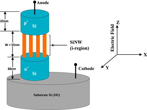
Figure 1. 3D SiNW pin structure.
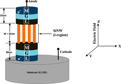
Figure 2. 3D MGL/SiNW-based pin structure.
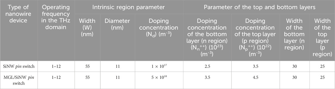
Table 1. Required design parameters of the proposed nanowire pin devices.
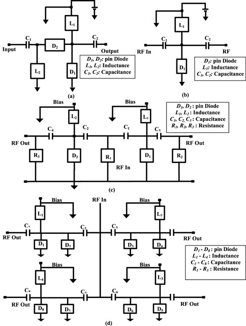
Figure 3. (A) Series-shunt SPST, (B) shunt SPST, (C) shunt SPDT, and (D) shunt SPMT—ultra fast pin switches for high-frequency operation.
2 Device modeling
This section describes the device modeling for the design and analysis of the switching characteristics of MGL/SiNW exotic pin switches in the THz frequency region. The non-linear RF characteristics of the device at THz frequencies are analyzed through the development of the QRSP-DD model by considering appropriate boundary conditions, simulation techniques, and the device’s structure details. The development of the QRSP-DD model, its design parameters, and non-linear RF characteristics are discussed in detail in Sections 2.1, 2.2, and 2.3 respectively.
2.1 Quantum-rectified Schrodinger–Poisson drift-diffusion model
The QRSP-DD model is developed based on the solutions to the Schrodinger–Poisson equation, in which quantum-potential (QP) is incorporated, and it can be expressed as (Falco et al., 2005)
In the intrinsic region, the effective mass of electron and hole changes along the z-axis, as depicted in Figures 1A, B. The working principle of the pin switch can be properly explained under biasing conditions. The switch reaches its ‘ON’ and ‘OFF’ state under forward bias and reverse bias conditions, respectively. Consequently, the effect of the biasing voltage (
In Equation 2,
where n is the concentration of the negatively charged carrier and can be represented as Equation 4.
In device modeling, the moderately doped intrinsic region and heavily doped p and n regions are divided into barriers and wells. Subsequently, the Schrodinger–Poisson equation can be expressed in the following form.
In Equation 5,
The kinetic energy term is split into two components: i. out-of-plane component and ii. in-plane component. The out-of-plane component is represented by
The actual energy for well and barrier can be written as shown in Equation 6.
During device modeling, the change in the effective potential in well and barrier regions of the device can be obtained by Equation 7.
where
The effective mass of the charged carriers in the well and barrier regions along in-plane and out-of-plane directions is given by (Greve, 2001; Ang et al., 2004) Equations 8a, 8b respectively.
In this device modeling, the wave function is represented by
In Equation 9, the periodicity of the Bloch function is denoted by
where
In Equation 5, the inclusion of position reliant effective mass
Applying the Ben Daniel–Duke boundary conditions, Equation 11 can be modified as
The assumption made in Equation 12 can be proven true as the total wave function,
The presumption made in Equation 13 affects the continuity of
In Equation 14,
Now, Equation 15 is solved by incorporating the appropriate boundary conditions, i.e.,
where d is the number of nanowires,
In Equation 17,
where
Due to the tunneling phenomenon, the electron and hole generation rate is expressed as Equations 21a–23,
In Equation 25,
In Equation 24, the ionization rate of electrons and holes is denoted by
In Equation 26, m represents the exponential co-efficient;
The induced electric field
2.2 Design parameters
The width (W) and doping concentration (
At the steady-state condition, the solution to Equation 28 is given by
where
In Equation 29,
The diffusion length (
In Equation 29,
where Nd represents the impurity concentration of the donor atoms; Na represents the impurity concentration of the acceptor atoms; and s represents the exponential incremental factor for the doping concentration at the vicinity of the junction.
The value of s varies from 3.5 nm to 4.5 nm to calculate the doping concentration of p and n regions.
2.3 Non-linear RF characteristics
The study of the non-linear switching characteristics of the proposed device has been performed through the development of the QRSP-DD model (coupled with a PSpice simulator). In this non-linear analysis, the large RF signal is applied to the developed QRSP-DD model by considering a 50% modulation index over the breakdown electric field. The switching performance, as well as the electrical characteristics of the DUT, is obtained by considering the iteration up to harmonics of the applied large RF signal, and it can be expressed as follows (Kundu et al., 2018):
Equation 33 indicates the variation in the RF signal over the DC breakdown voltage. The equivalent circuit of nanowire SPST switches is analyzed at THz frequency by considering the voltage excitation approach of the non-sinusoidal RF signal. The component of large-RF-signal can be expressed as
The V–I characteristics of the proposed DUT, which can be derived using Equation 34, yield the ideal values for DC current and breakdown voltage.
Equation 34 denotes the reverse saturation current of the proposed DUT. The charged particles are injected into the intrinsic region under forward bias conditions. The product of the carrier lifetime (τ) and the current flowing across the DUT under forward bias conditions yields the number of injected charged particles (Q) (Kundu et al., 2018). These injected charged particles move toward the anode and cathode under the biasing conditions. However, some of the charged particles remain in the intrinsic region. It can be eliminated by applying a reverse recovery process. The reverse recovery mechanism causes the instantaneous reverse-transit current (i(t)) to begin flowing across the DUT. The transit-current component (i(t)) is an important factor in power dissipation in the DUT. Therefore, the analysis of the DUT’s transit-time behavior is crucial for modeling the high-frequency device, and it can be represented as (Leenov, 1963)
In Equation 35,
The solution to the 2-D carrier transport equation yields the RF resistance. The value of the RF resistance depends on the magnitude of the intrinsic region’s resistance (
Another important factor for the analysis of the switching behavior of the DUT is power dissipation
In Equation 38,
Furthermore, the analysis of the SPST switch’s switching characteristics in the RF frequency region of the electromagnetic spectrum considers all these significant device parameters. Employing the combination of the QRSP-DD model and PSpice simulator, the switching characteristics of the device are obtained, taking into account the appropriate values of parasitic elements (Figures 3A–C). The proposed device-based SPST switch with series-shunt and shunt configurations is shown in Figures 4A–C.
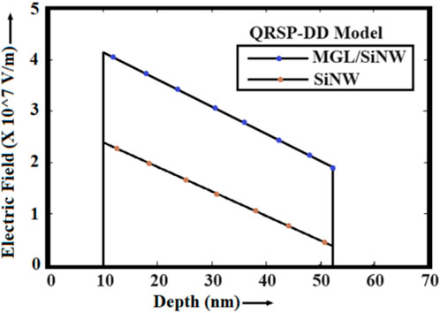
Figure 4. Induced electric field profile of SiNW and MGL/SiNW pin devices obtained from the QRSP-DD model.
The expressions are provided as Kundu and Mukherjee, 2022; Bellantoni et al., 1989 shown in Equations 39–42.
3 Results and discussion
In this section, the electrical characteristics of the DUTs and the performance of the switches are analyzed using the developed QRSP-DD model in conjunction with PSpice software. The authors have also divided this section into two subsections to describe the results and analysis in detail.
3.1 Electrical characterization of the DUTs
In this section, the authors investigate the electrical characteristics of the DUTs. The induced electric field in the i-region plays an important role in the separation of the charged carriers and enhancement of the conductivity of the device. This phenomenon plays an important role in increasing the overall performance of the solid-state switch. It is analyzed for a complete period of oscillation, i.e., 0 to
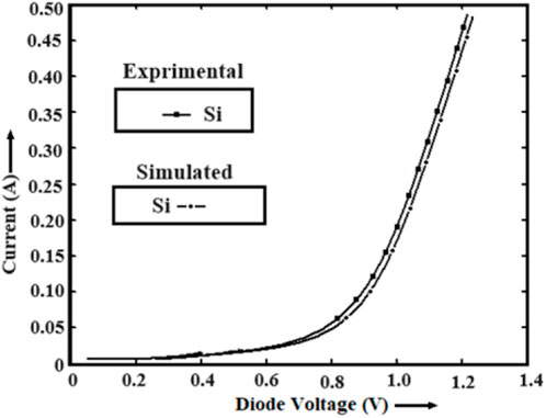
Figure 5. Variation in the diode current of the Si-based pin device at room temperature under experimental and simulated conditions.
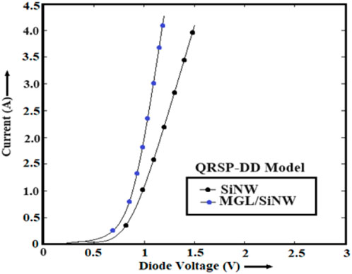
Figure 6. Variation in the device current under the forward bias condition.
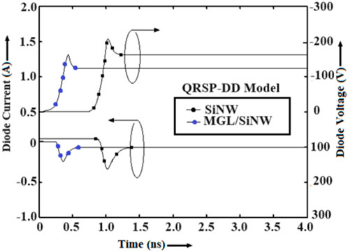
Figure 7. Reverse recovery current component for strained and unstrained Si-based pin devices under simulation conditions.
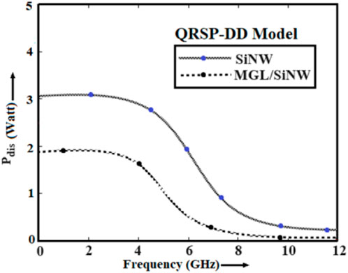
Figure 8. RF resistance of SiNW and MGL/SiNW pin devices obtained from the QRSP-DD model.
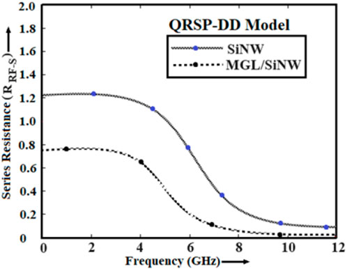
Figure 9. Power dissipation of SiNW and MGL/SiNW pin devices obtained from the QRSP-DD model.
3.2 Analysis of the switching characteristics of the series-shunt SPST and shunt SPST, SPDT, and SPMT switches
In this section, the authors have investigated the switching characteristics of the series-shunt and shunt SPST switches. The switching characteristics of the devices are studied in the THz frequency domain in terms of IL and ISO using the PSpice simulator coupled with the developed QRSP-DD model. The low insertion loss and high isolation can enhance the switching performance of the device at high-frequency operation. Hence, the optimization of these parameters is a challenging task for the device engineers. The authors have checked the model’s validity by analyzing the experimental observations and simulated data obtained from the PSpice simulator coupled with the QRSP-DD model in a similar operating environment (Henfiner et al., 2001). The authors have used the same model to analyze the switching characteristics of the devices in the THz frequency domain. The experimental observations and simulated data of IL and ISO with the variations in frequency in the microwave region are shown in Figures 10, 11, respectively. It is observed from Figures 10, 11 that the simulated data taken from the QRSP-DD model are similar to the actual data obtained from experimental observation. The abovementioned study clarifies the superiority of the developed model. In addition, the switching performance in terms of IL and ISO of the designed device-based series-shunt and shunt SPST switches are shown in Figures 12, 13, respectively, and shunt SPST and SPMT switches are shown in Figures 14, 15, respectively. It is observed from Figure 12 that the IL is 0.0052 dB at 5 THz frequency in the case of the MGL/SiNW-based shunt SPST switch. It is also observed from Figure 13 that ISO is −79.52 dB at 5 THz frequency in the case of the MGL/SiNW-based shunt SPST switch. The abovementioned discussion reveals the superiority of MGL/SiNW-based shunt SPST switches over their SiNW counterpart.
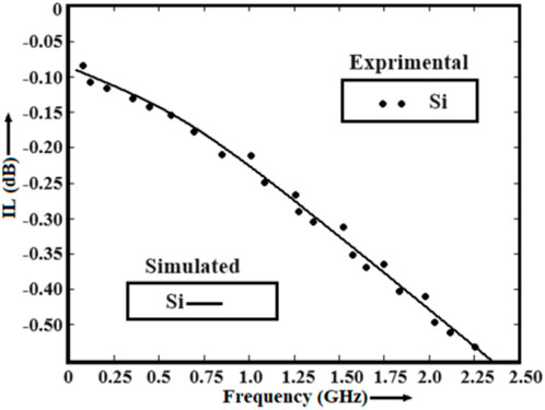
Figure 10. IL of Si pin devices under experimental and simulation conditions.
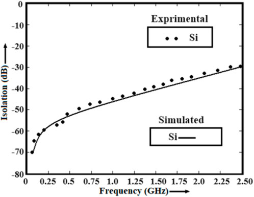
Figure 11. ISO of Si pin devices under experimental and simulation conditions.
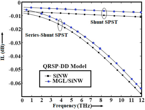
Figure 12. IL of SiNW and MGL/SiNW pin device-based series-shunt SPST and shunt SPST switches.
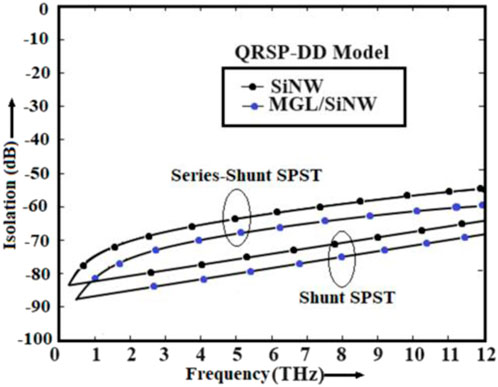
Figure 13. ISO of SiNW and MGL/SiNW pin device-based series-shunt SPST and shunt SPST switches.
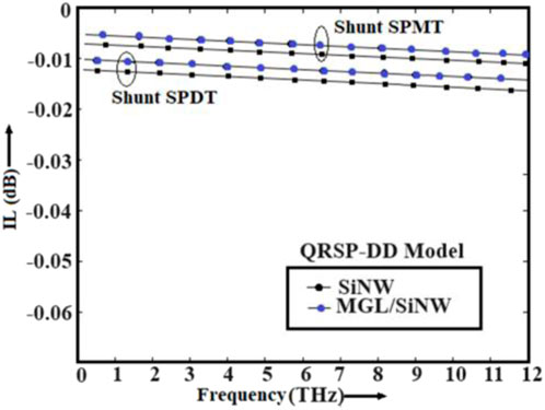
Figure 14. IL of SiNW and MGL/SiNW pin device-based shunt SPDT and shunt SPMT switches.
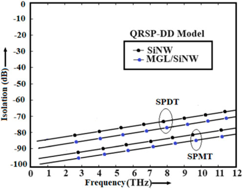
Figure 15. ISO of SiNW and MGL/SiNW pin device-based shunt SPDT and shunt SPMT switches.
It is also observed from Figure 14 that the IL is significantly small (0.007 dB) at 5 THz frequency in the case of the MGL/SiNW-based shunt SPMT switch compared to the shunt SPDT switch. On the other hand, ISO is significantly high (91.15 dB) at 5 THz frequency in the case of the MGL/SiNW-based shunt SPMT switch, as observed in Figure 15. Hence, this investigation reveals the superiority of the MGL/SiNW-based SPMT switch in the THz frequency region.
4 Proposed fabrication model of the device
The authors established multi-graphene layer/Si nanowire pin-based series-shunt and shunt SPST, SPDT, and SPMT switches in the THz frequency range. The electrical characteristics of graphene make it suitable for switching applications in the THz frequency range.
The heterostructure graphene/Si nanowire switch can be fabricated using the molecular beam epitaxy (MBE) method, which allows the creation of abrupt and flat hetero-interfaces. From the maturity and cost efficiency perspective, Si (100) could be chosen as a substrate material for developing the epitaxial layer of graphene and Si according to the device’s design. Ohmic contacts with low resistance could be developed using the plasma etching process, followed by the rapid thermal annealing (RTA) process.
Low-resistive metals like Ni/Ti/Au could be chosen for developing cathode terminals on the heavily doped n-type multi-graphene layer. Ni could be selected to develop the anode terminal on the heavily doped p-type multi-graphene layer. The mesa-structure of the device could be formed using photolithography and lift-off processes. The proposed fabrication model of the device is shown in Figure 16.
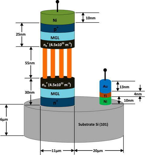
Figure 16. Proposed fabrication model of the MGL/SiNW pin switch.
5 Conclusion
The performance of SiNW exotic MGL/SiNW pin device-based SPST, SPDT, and SPMT switches is analyzed in terms of insertion loss and isolation in the THz frequency domain. From this comprehensive study, it has been observed that exotic MGL/SiNW pin device-based SPMT switches offer low insertion loss and high isolation compared to their SiNW counterparts in the THz frequency domain. Hence, the superiority of the exotic MGL/SiNW pin switch is established for application in the THz frequency domain. This study is very useful in the field of device engineering for the development of high-frequency switches and detectors.
Data availability statement
The original contributions presented in the study are included in the article/Supplementary Material; further inquiries can be directed to the corresponding author.
Author contributions
SB: writing–original draft and writing–review and editing. AK: writing–original draft and writing–review and editing. JK: writing–review and editing and writing–original draft. AS: writing–review and editing. MM: software, supervision, validation, and writing–review and editing.
Funding
The author(s) declare that no financial support was received for the research, authorship, and/or publication of this article.
Conflict of interest
The authors declare that the research was conducted in the absence of any commercial or financial relationships that could be construed as a potential conflict of interest.
Publisher’s note
All claims expressed in this article are solely those of the authors and do not necessarily represent those of their affiliated organizations, or those of the publisher, the editors and the reviewers. Any product that may be evaluated in this article, or claim that may be made by its manufacturer, is not guaranteed or endorsed by the publisher.
References
Ang, K. W., Chui, K. J., Blimetsov, V., Du, A., Balasubramanian, N., Li, M. F., et al. (2004). Enhanced performance in 50 nm N-MOSFETs with silicon–carbon source/drain regions. IEDM technical digest. IEEE Int. Electron. Dev. Meet. doi:10.1109/IEDM.2004.1419383
Bellantoni, J. V., Bartle, D. C., Payne, D., McDermott, G., Bandla, S., Tayrani, R., et al. (1989). Monolithic GaAs p-i-n diode switch circuits for high-power millimeter-wave applications. IEEE Trans. Microw. Theory Tech. 37, 2162–2165. doi:10.1109/22.44137
Bogle, J. J., Hubert, R. J., and Boles, T. E. (2010). “A 50 watt monolithic surface-mount series-shunt pin diode switch with integrated thermal sink,” in Proceeding of Asia-Pacific Conference, USA, 07-10 December 2010.
Boles, T., Brogl, J., and Hong, D., (2013). AlGaS anode hetero-junction pin diodes. Wiley 10, 786–789. doi:10.1002/pssc.201200612
Buder, T., Kinayman, T., and Yong-Hoon, Y. (2003). Low-loss high-isolation 60-80 GHz GaAs SPST pin switch. IEEE MTT-s Dig., 1307–1310. doi:10.1109/MWSYM.2003.1212610
Camara., N., and Zekentes, H. (2006). Microwave pin diode and switches based on 4H-SiC. IEEE Electron Device Lett. 27, 108–110. doi:10.1109/LED.2005.862686
Egorov, I., Xiao, Y., and Poloskov, A. (2018). Pin diode diagnostics of pulsed electron beam for high repetition rate model. J. Phys. Conf. Ser. 830, 0120044. doi:10.1088/1742-6596/755/1/011001
Falco, C. D., Gatti, E., Lacaita, A. L., and Sacco, R. (2005). Quantum-corrected drift-diffusion models for transport in semiconductor device. J. Comput. Phys. 204, 533–561. doi:10.1016/j.jcp.2004.10.029
Greve, D. W. (2001). Si–Ge–C growth and devices. Mater. Sci. Eng. B 87 (3), 271–276. doi:10.1016/S0921-5107(01)00724-3
Hadi, M. H., Ahmad, B. H., and Shairi, N. A. (2013). “Effect of discrete pin diode on defected ground structure,” in Wireless technology and applications (ISWTA)”, IEEE symposium, 333–337.
Henfiner, A. R., Singh, R., Lai, J. S., Berning, D.W., Chapuy, C., et al. (2001). SiC power diode provide breakthrough performance for a wide range of application. IEEE Trans. 16, 273–278. doi:10.1109/63.911152
Johon, D. L., Pulfrey, D. L., and Castrol, L. C., (2004). Quantum capacitance in nanoscale device modelling. J. Appl. Phys. 96, 5180. doi:10.1063/1.1803614
Kundu, A., Bhattacharya, S., Chakraborty, D., Chakraborty, S., and Mukherjee, M. (2021b). Strain—engineered asymmetrical Si/Si1–xGex IR-photo-detector: theoretical reliability and experimental feasibility studies. IEEE Trans. Device Mater. Reliab. 21 (4), 627–638. doi:10.1109/TDMR.2021.3125452
Kundu, A., Kanjilal, M., and Mukherjee, M. (2021a). Cubic versus hexagonal SiC vertical pin SPST/SPDT/SPMT switches for MMW communication systems: a modified quantum drift-diffusion model for switching characteristics analysis. Microsyst. Technol. 27, 387–406. doi:10.1007/s00542-019-04445-9
Kundu, A., Kanjilal, M. R., and Mukherjee, M. (2018). III-V super-lattice SPST/SPMT pin switches for THz communication: - theoretical and experimental feasibility studies. Microsyst. Technol. 27, 539–541. doi:10.1007/s00542-018-4053-5
Kundu, A., Kundu, J., Modak, D., and Mukherjee, M. (2019). Quantum modified drift-diffusion modeling of vertically doped asymmetrical pin switches for application in MMW system. AIP Conf. Proc. 2072. doi:10.1063/1.5090241
Kundu, A., and Mukherjee, M. (2022). Physics based non-linear large-signal analysis of multiple-graphene layer exotic pin (p++–n−–n–n++) devices and ultra-fast SPST/SPDT/SPMT switches on Si/3C-SiC (100) substrates for application in THz-communication. Microsyst. Technol. 28, 683–704. doi:10.1007/s00542-019-04325-2
Leenov, D. (1963). ―The silicon pin diode as a microwave rader protector at megawatt level. IEEE Trans. Electron Devices 10, 53–61. doi:10.1109/T-ED.1964.15283
Mamedes, D. F., and Bornemann, J. (2021). High-gain reconfigurable antenna system using PIN-Diode-Switched frequency selective surfaces for 3.5 GHz 5G application. 2021 SBMO/IEEE MTT-S Int. Microw. Optoelectron. Conf. (IMOC), 1–3. doi:10.1109/imoc53012.2021.9624918
Ng, M.-F., Zhou, L., Yang, S., Sim, L. Y., Tan, V. B. C., and Wu, P. (2007). Theoretical investigation of silicon nanowires: methodology, geometry, surface modification, and electrical conductivity using a multiscale approach. Phys. Rev. B 76, 155435. doi:10.1103/PhysRevB.76.155435
Novoselov, K. S., Geim, A. K., Morozov, S. V., Jiang, D., Zhang, Y., Dubonos, S. V., et al. (2004). Electric field effect in atomically thin carbon films. Science 306, 666–669. doi:10.1126/science.1102896
Oberlin, A., Endo, M., and Koyama, T. (1976). Filamentous growth of carbon through benzene decomposition. J. Cryst. Growth 32, 335–349. doi:10.1016/0022-0248(76)90115-9
Paz-Martínez, G., Trevino-Palacios, C. G., Molina-Reyes, J., Romero-Moran, A., Cervantes-Garcia, E., Mateos, J., et al. (2021). Influence of laser modulation frequency on the performance of terahertz photoconductive switches on semi-insulating GaAs exhibiting negative differential conductance. IEEE Trans. Terahertz Sci. Technol. 11 (5), 591–597. doi:10.1109/TTHZ.2021.3083926
Pinping, S., Wang, L., and Upadhyaya, U., (2005). High isolation 10HHz to 20GHZ SPDT switches design using novel octagonal pin diode structure. Microelectron. Electron Devices WMED 38, 15. doi:10.1109/WMED.2005.1431612
Pratt, I., and Oliver, M. (2021). “Performance of PIN diode RF switches within HF RFID reader designs,” in 2021 IEEE International Conference on RFID Technology and Applications (RFID-TA), USA, 6-8 Oct. 2021, 289–292. doi:10.1109/rfid-ta53372.2021.9617334
Sze, S. M. (2008). Semiconductor devices: physics and technology. 2nd Edition. New York: Willey. doi:10.1002/0470068329
Takahashi, K., Okamura, S., Wang, X., et al. (2011). “A capacitance compensated high isolation and low insertion loss series pin diode SPDT switch,” in Proceeding of the 41st European microwave communication (IEEE), 583–586. Available at: https://ieeexplore.ieee.org/document/6101964/.
Tomioka, K., Ikejiri, K., Tanaka, T., Motohisa, J., Hara, S., Hiruma, K., et al. (2011). Selective-area growth of III-V nanowires and their applications. J. Mater. Res. 26 (17), 2127–2141. doi:10.1557/jmr.2011.103
Tomioka, K., Kobayashi, Y., Motohisa, J., Hara, S., and Fukui, T. (2009). Selective-area growth of vertically aligned GaAs and GaAs/AlGaAs core-shell nanowires on Si(111) substrate. Nanotechnology 20 (14), 145302. doi:10.1088/0957-4484/20/14/145302
Xu, Y., Yuan, X., Ye, F., Wang, Z., Zhang, Y., Diab, M., et al. (2021). Impact of high switching speed and high switching frequency of wide-bandgap motor drives on electric machines. IEEE Access 9, 82866–82880. doi:10.1109/ACCESS.2021.3086680
Yang, Z., Yang, T., You, Y., and Xu, R. (2005). A 2GHz high isolation DPDT switches MMIC microwave proceeding. APMC, Asia Parcific Conf. Proceeding 2, 4–7. doi:10.1109/APMC.2005.1606503
Glossary
h Planck’s constant
Uunit-s unit step function
W width of the i-region
Nd impurity concentration of the donor atoms
Na impurity concentration of acceptor atoms
S exponential incremental factor for the doping concentration at the vicinity of the junction
Keywords: multi-graphene layer/Si nanowire, quantum rectified Schrodinger–Poisson drift-diffusion model, RF series resistance, insertion loss, isolation
Citation: Bhattacharya S, Kundu A, Kundu J, Sarkar A and Mukherjee M (2025) MGL/SiNW-based exotic pin switch with low insertion loss and high isolation for THz communication: a quantum-rectified Schrodinger–Poisson drift-diffusion model for the design and analysis of switching behavior. Adv. Opt. Technol. 14:1474728. doi: 10.3389/aot.2025.1474728
Received: 02 August 2024; Accepted: 15 January 2025;
Published: 12 February 2025.
Edited by:
Rajesh Sharma, Guru Ghasidas Vishwavidyalaya, IndiaReviewed by:
Huseyin Canbolat, Ankara Yıldırım Beyazıt University, TürkiyeReena Sharma, Indian Institute of Technology Ropar, India
Copyright © 2025 Bhattacharya, Kundu, Kundu, Sarkar and Mukherjee. This is an open-access article distributed under the terms of the Creative Commons Attribution License (CC BY). The use, distribution or reproduction in other forums is permitted, provided the original author(s) and the copyright owner(s) are credited and that the original publication in this journal is cited, in accordance with accepted academic practice. No use, distribution or reproduction is permitted which does not comply with these terms.
*Correspondence: Abhijit Kundu, YWJoaWppdHVkYXlAeWFob28uY28uaW4=