 Mingxi Chen
 Tsung-Tse Lin1,3
- 1Terahertz-Wave Research Group, RIKEN Center for Advanced Photonics, Sendai, Japan
- 2Department of Physics, Graduate School of Science, Tohoku University, Sendai, Japan
- 3Research Institute of Electrical Communication, Tohoku University, Sendai, Japan
Introduction:: Surface-emitting terahertz quantum cascade lasers (THz QCLs) are highly promising for applications requiring high-quality far-field beams and controlled beam divergence. However, limited brightness and output power in conventional surface-emitting designs remain significant barriers to practical implementation. Although photonic crystal structures and distributed Bragg reflectors have been explored to enhance surface emission, intrinsic limitations in emission area scaling and brightness improvement persist. Thus, new strategies are essential to advance the performance of surface-emitting THz QCLs.
Methods:: This study proposes a plasma-assisted photonic crystal waveguide design to improve surface emission efficiency in THz QCLs. A three-dimensional TM-mode coupled wave theory (3D TM-mode CWT) model was developed, incorporating effective permittivity enhancement and a self-consistent iterative scheme to accurately simulate optical field distribution and interaction within the structure.
Results:: Simulations reveal that the introduction of a plasma layer effectively disrupts the optical field symmetry characteristic of conventional double-metal waveguides, promoting vertical emission. Through systematic optimization, a plasma layer thickness of 0.8 μm was identified as having the potential to achieve surface emission efficiencies exceeding those of conventional structures by over two orders of magnitude. This enhancement is realized without significantly increasing fabrication complexity.
Discussion:: The plasma-assisted photonic crystal waveguide design offers a viable pathway toward realizing high-brightness surface-emitting THz QCLs. Although challenges such as material growth control and thermal management remain, the substantial improvement in surface emission efficiency underscores the potential of this approach for future high-performance terahertz applications.
1 Introduction
Terahertz quantum cascade lasers (THz QCLs) have demonstrated significant potential in various fields such as non-destructive testing, biological research, and high-speed communications due to their compact size, strong coherence, and high energy conversion efficiency (Chan et al., 2007; Scalari et al., 2009; Tao et al., 2020; Williams, 2007). In recent years, THz QCLs have achieved a maximum output power exceeding 1 W and an operating temperature of 265 K (Khalatpour et al., 2023; Li et al., 2017; Lin et al., 2022), marking a significant step towards practical applications. However, traditional edge-emitting THz QCLs face severe diffraction issues, resulting in poor far-field beam quality (Fathololoumi et al., 2010; Shao et al., 2021). Recent studies have demonstrated improved far-field performance by incorporating novel external structures such as silicon lenses (Wan et al., 2018). Yet, improving the intrinsic surface emission efficiency of the laser cavity itself remains a promising direction. Additionally, current THz QCLs hard to achieve both high brightness and high operating temperatures, particularly near room temperature. THz QCLs only achieve milliwatt-level brightness at relatively high-operating temperature (Khalatpour et al., 2021; Khalatpour et al., 2023; Lin et al., 2017). Consequently, improving far-field beam quality and radiation power has become a critical challenge for the practical application of THz QCLs.
Surface-emitting THz QCLs based on photonic crystal structures have shown unique advantages in enhancing far-field beam quality and radiation power (Colombelli et al., 2003; Czyszanowski, 2018; Liang et al., 2014). Compared to traditional lateral emission designs, surface-emitting lasers have a larger light extraction area, significantly improving far-field patterns and achieving higher radiation power. Moreover, due to the periodic spatial arrangement of the photonic crystal structures, these lasers also exhibit superior single-mode operation capabilities (Li et al., 2018). Despite these advantages, the realization of high-power surface-emitting THz QCLs remains elusive due to the low light extraction efficiency of waveguides, which has been a major challenge in this research area over the past decade.
We believe that developing appropriate simulation methods and gaining a deeper understanding of the optical field behavior in photonic crystal surface-emitting THz QCLs are key to addressing this challenge. Traditional numerical simulation methods, such as the finite-difference time-domain (FDTD) method and finite element method (FEM) (Colombelli et al., 2003; Yokoyama and Noda, 2005), while generally reliable, consume significant computational resources and introduce numerical dispersion when dealing with extreme permittivitycontrasts (Liu and Chang, 2013), making it difficult to explore a large number of potential designs within a limited time. In particular, THz QCLs often involve materials with large absolute permittivity values, negative real parts, and strong permittivitycontrast. These features make it extremely challenging to simulate non-standard structures—such as those employing heavily doped layers to modulate optical field distributions—using conventional methods. Furthermore, such numerical methods typically provide only superficial insight into electromagnetic behavior. They offer limited physical interpretability and make it difficult to identify the root causes of the low light extraction efficiency observed in many surface-emitting THz QCL structures.
In our previous work (Chen et al., 2025), we extended a method known as three dimensional TM-mode Coupled Wave Theory (3D TM-mode CWT) (Liang et al., 2013; Liang et al., 2011; Peng et al., 2011) to accurately and rapidly simulate optical field distributions in THz QCLs, providing clear physical insights. This method allowed us to delve into the intrinsic mechanisms of surface-emitting THz QCLs. Our research revealed that the low efficiency of current surface-emitting THz QCLs is primarily due to the high reflectivity of the upper and lower waveguides, leading to highly symmetrical upward and downward optical fields. This symmetry causes the optical fields to cancel each other out, preventing effective surface emission.
To overcome this limitation, we propose inserting a plasma layer, much thicker than the contact layer, at the back of the waveguide to break this symmetry. This design significantly enhances surface emission capabilities, achieving an efficiency that is a hundred times greater than traditional designs. By comparing our results with those obtained from the FDTD method, we verified the accuracy of our approach and, for the first time, successfully identified the reasons for the low light extraction efficiency of current surface-emitting THz QCLs compared to surface-emitting lasers in other wavelength bands. Our study also demonstrates the potential application of the enhanced TM-mode 3D CWT, coupled with a plasma layer and self-consistent iteration, as an effective simulation tool in the research of photonic crystal surface-emitting lasers, including surface-emitting THz QCLs.
2 Enhanced TM-mode 3D CWT as the simulation method
Traditional 3D TM-mode CWT models face significant numerical dispersion issues when dealing with metal waveguide structures. These issues arise primarily due to the extreme permittivities of metallic materials, leading to instability in numerical calculations. To overcome these challenges, we introduced the Effective Permittivity Enhanced (EPE) model, which is employed to describe the influence of the metal, thereby avoiding the direct calculation of metallic media. This approach simplifies the problem while maintaining high accuracy. The self-consistent iteration further enhances our model by allowing iterative refinements of the initial calculations, progressively approaching the true physical solution. This iterative process effectively handles the coupling effects of higher-order waves, thereby improving the accuracy and convergence of the simulation results. For further technical details, please refer to our previous work (Chen et al., 2025).
3 Simulation results and discussion
3.1 Traditional structures
In our simulations, we selected four typical photonic crystal structures: circular and right-angled triangular air holes, as well as two dual-lattice structures proposed in recent years. These structures have demonstrated effective functionality in surface-emitting semiconductor lasers. The filling factor of the air holes (the ratio of the air hole area to the waveguide area) ranged from 0.01 to 0.15. Larger air holes can weaken waveguide confinement and cause uneven current injection, damaging the device (Chassagneux et al., 2009).
In principle, increasing the lateral dimensions of the device (in the x and y directions) improves surface emission power. For sufficiently large devices, we simplify the simulation by assuming ideal periodic boundary conditions for the repeating photonic crystal unit cells.
It is well known that the permittivity of materials in the terahertz regime is strongly frequency dependent. To obtain the permittivity values used in our simulations, we adopted the Drude model. Materials were categorized into three types: metal, heavily doped GaAs, and intrinsic GaAs used in the active region. We then calculated their theoretical permittivities at 3.5 THz. The resulting complex permittivities were: metal, −183,000 + 167000i; heavily doped n++ GaAs, approximately −394 + 185i; and intrinsic GaAs, approximately 12.6. To avoid the complications of dispersion in our model, we used these values to construct an equivalent permittivity approximation for the simulations, following the approach in our previous work (Chen et al., 2025). Other detailed simulation parameters of structure are shown in Figure 1.
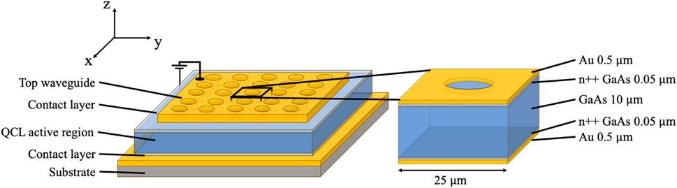
Figure 1. A sketch diagrams of (Left) surface-emitting THz QCL, and (Right) single unit cell within the photonic crystal is used for our calculations. We assume that the device is large enough to allow the unit cells to have ideal periodic boundary conditions along the x-y directions. The unit cell size is set to 25 μm, targeting an operating frequency around 3.5 THz—typical for THz QCLs.
The simulation results show that, for all investigated structures, the frequencies of modes A and B shift, indicating mode coupling within the waveguide. However, the corresponding surface emission coefficients remain close to zero (as shown in Figure 2), reflecting poor surface radiation efficiency in standard double metal waveguides. This observation is consistent with our previous findings.
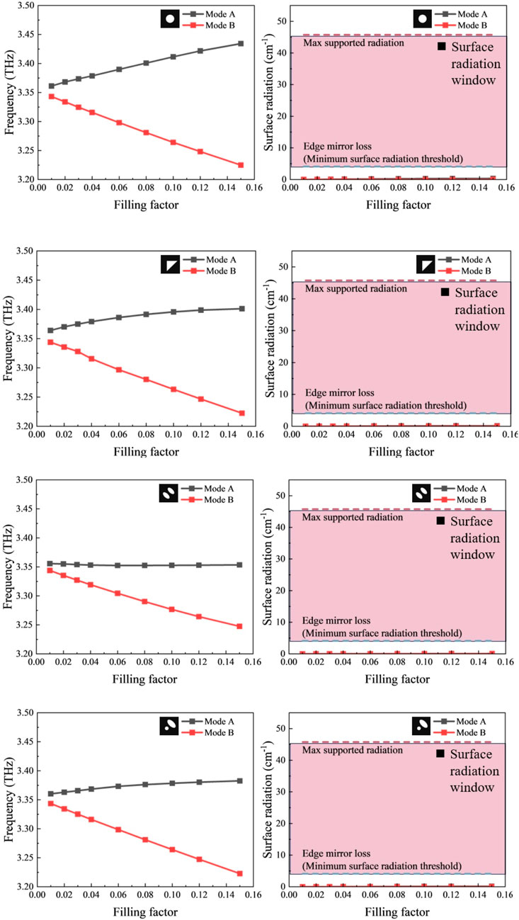
Figure 2. Simulation results for four representative surface-emitting photonic crystal designs. The different photonic crystal designs are indicated in the top right corner of the data plots: black regions represent the metal-covered areas, while white regions denote the air node areas. Modes A and B are the two highly efficient anti-symmetric modes typically considered in surface-emitting photonic crystals. We assume a gain of 50 cm-1 for the THz QCLs, which is a conservative estimate, and an edge mirror loss of 4 cm−1. For the laser to achieve successful lasing with surface radiation dominating the device behavior, the surface radiation loss must lie between 46 cm−1 and 4 cm−1; this range is referred to as the “surface radiation window.” The results show that, even under ideal conditions with a sufficiently large device, electromagnetic coupling between the waveguides causes a frequency shift in modes A and B, but none of the structures effectively extracts light from the surface in any mode.
These results collectively confirm that conventional double metal waveguide structures inherently suffer from low surface emission efficiency. Even in large-area devices where periodic boundary conditions can be reasonably assumed, strong in-plane (x–y) coupling within the photonic lattice significantly suppresses vertical radiation. Although the infinite-length approximation may slightly underestimate the absolute emission efficiency, it does not alter the main conclusion. For example, even in advanced designs such as (Li et al., 2024) the surface emission coefficient remains around 6 cm-1. This underscores the fundamental inefficiency of these structures for surface emission applications.
To better understand this behavior, we further examined the physical origin of surface emission in TM-mode devices. In typical THz QCLs, which operate in TM mode, the magnetic field components lie primarily in the lateral (x–y) directions, while the electric field component is oriented along the vertical (z) axis. For surface emission to occur, a portion of the electric field must be deflected into the horizontal plane (Kumar, 2007). This deflection typically arises from structural perturbations such as air nodes in photonic crystals. According to the Poynting vector expression
For clarity, we denote the local directions of the magnetic and electric fields as
Under the single-frequency approximation commonly used for laser modes, the transverse electric field can be further expressed as:
where
However, our simulations show that in conventional double metal waveguides, the magnetic field distribution along the z-axis remains nearly uniform (see Figure 3, curve labeled “Double Metal”). This implies that
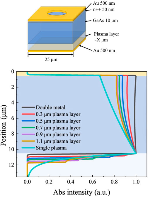
Figure 3. Improved unit cell structure. A plasma layer formed by a heavily doped semiconductor is inserted between the bottom metal waveguide and the active layer. For the calculations, we used an n++ doping type with a concentration of 5 × 1018 cm−3. The right side shows the longitudinal optical field distribution of the basic mode after inserting different plasma layers. The bottom waveguides of the various structures are not color-coded and are simply represented by white regions.
This phenomenon can be attributed to the subwavelength thickness of the waveguide, which limits vertical photon momentum, similar to the well-known diffraction behavior observed in narrow slits. In double metal structures, both the top and bottom metal layers act as nearly perfect reflectors. As a result, the upward and downward propagating waves are highly symmetric and tend to cancel each other’s phases in the vertical direction. Consequently, the electromagnetic energy is largely confined to horizontal propagation, and efficient surface emission through photonic crystal coupling becomes fundamentally difficult in such configurations.
3.2 Plasma layer assisted surface emission structures
Another widely used waveguide form in THz QCLs is the single plasma layer waveguide. Unlike double metal waveguides, its bottom layer is not metal but consists of a highly doped GaAs layer. Due to the significant permittivitycontrast between the upper metal layer (with a permittivity of approximately −106) and the lower highly doped layer (approximately −102), the longitudinal optical field distribution exhibits a noticeable tilt, as shown in Figure 3 (labeled by ‘Single plasma’). This observation suggests that we can avoid phase cancellation effects caused by high symmetry by adjusting the thickness of the bottom highly doped layer, thereby controlling the coupling efficiency of the surface emission coefficient.
However, single-plasma waveguide structures are not suitable for surface emission directly. The reason is that as the thickness of the heavily doped layer increases, it strongly absorbs the longitudinally propagating optical field. In our design, which aims for significantly higher surface emission efficiency than edge-emitting configurations, this absorption introduces a substantial loss. Moreover, the vertical component of the Poynting vector implies that surface-emitted energy may increasingly penetrate the doped region, leading to even greater losses. As a result, the optical gain provided by the active region may be insufficient to sustain lasing. This necessitates a new structural approach.
To address this, we introduce a hybrid structure that combines features of double metal and single-plasma waveguides. This design is feasible because highly doped layers already exist in both waveguide types. In addition to smoothing the Fermi level and facilitating electron injection, the doped layer also serves as part of the optical confinement. Importantly, the presence of a bottom metal layer and a relatively thinner doped layer—compared to conventional single-plasma designs—ensures sufficient reflectivity and avoids excessive backside optical absorption.
Based on these considerations, we introduced a plasma layer of varying thickness, from 0.1 μm to 1.1 μm. As previously discussed in the context of single-plasma waveguides, thicker plasma layers can lead to strong absorption of the longitudinally propagating optical field, reducing light extraction efficiency. To evaluate the effect of layer thickness on surface emission, we used the right-angled triangular air hole structure as a representative example (Figure 4).
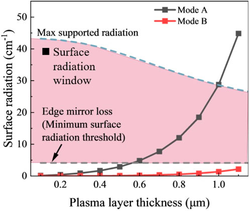
Figure 4. Simulation results showing the effect of varying the plasma layer thickness on surface radiation efficiency with a cylindrical air node and a fixed filling factor of 0.05. It is evident that changes in plasma layer thickness alter the surface radiation efficiency. The maximum supported radiation decreases with increasing plasma layer thickness, primarily due to the absorption effect of the plasma layer on the optical field.
Simulation results confirm that the introduction of a plasma layer significantly improves the surface emission coefficient across all examined photonic crystal designs. Moreover, as expected, a larger air hole area leads to more surface-emitted power. To further evaluate device feasibility, we illustrate in Figure 4 two horizontal dashed lines. The upper dashed line represents the maximum allowable radiation loss that can still be compensated by gain, considering both lateral mirror loss and optical absorption in the doped plasma layer. The lower dashed line corresponds to the lateral mirror loss alone. Surface emission becomes observable only when the radiation loss lies between these two thresholds. In this case, the device not only satisfies the condition for stimulated emission but also exhibits surface emission that dominates over lateral emission. The shaded pink region between the two dashed lines therefore defines the “surface radiation window.” In our calculation, we assume a typical gain of 50 cm−1 provided by the active region and a lateral mirror loss of approximately 4 cm−1. The absorption introduced by the heavily doped layer is estimated using the Transfer Matrix Method (TMM) (Vassell, 1974). As the plasma layer thickness increases, the maximum tolerable radiation loss decreases, due to enhanced absorption of the vertically propagating optical field by the thicker doped region.
Among the tested configurations, a plasma layer thickness of 0.8 μm was found to provide the best overall performance. It maintains the surface emission coefficient below the transverse mirror loss across multiple filling factors, thus ensuring efficient operation. This moderate coefficient also provides tolerance for variations in fabrication and design parameters. To further validate this configuration, we investigated four representative photonic crystal patterns using a fixed 0.8 μm plasma layer, while varying the filling factor in each case (Figure 5).
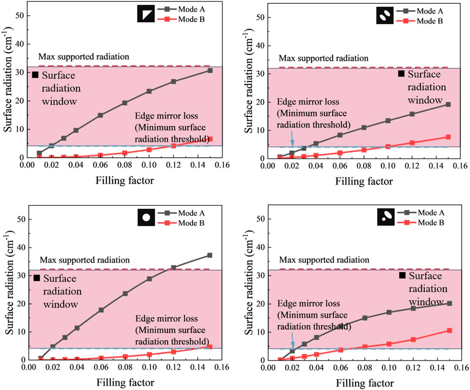
Figure 5. Simulation results for different photonic crystal designs with a fixed plasma layer thickness of 0.8 μm. A significant enhancement in surface radiation efficiency is observed across all four examined structures.
Notably, for circular air holes, despite their high symmetry—typically leading to cancellation of surface emission in anti-symmetric modes—we observed surface emission coefficients comparable to or even higher than those for right-angled triangular holes. This behavior differs from results reported in other wavelength regimes using conventional structures. It is not a numerical artifact, but instead arises from the use of a thicker plasma layer. While the layer has negative permittivity, part of the electric field can penetrate the doped plasma region and be reflected by the bottom metal. This introduces complex phase shifts in the electromagnetic field, leading to different coupling behavior. This effect is consistent with the guided-mode complex amplitude distributions obtained via the TMM.
Although a 0.8 μm doped layer is significantly thicker than typical THz QCL designs (∼0.05 μm), and may introduce stronger lattice mismatch, we believe this challenge remains manageable using modern MBE growth techniques, such as incorporating strain-relief buffer layers. Additionally, the increased vertical optical energy penetration in the plasma layer is expected to cause more pronounced thermal effects compared to traditional waveguide designs. Thus, improved thermal management strategies will be required. Despite these challenges, the substantial gain in surface emission efficiency makes this hybrid structure a compelling research direction.
4 Conclusion
This study proposes a plasma layer-assisted photonic crystal waveguide design, aiming to significantly enhance the radiation efficiency of surface-emitting THz QCLs through computational analysis. We introduced an innovative structure combining traditional double metal waveguides with single plasma layer waveguides and conducted detailed simulation calculations using an extended 3D TM-mode CWT. The simulation results demonstrate that the introduced plasma layer can effectively break the symmetry of the upper and lower waveguides, significantly enhancing the coupling efficiency of the optical field, thereby potentially increasing the radiation power of surface emission.
This study proposes a novel photonic crystal waveguide design that incorporates a plasma layer to enhance surface emission efficiency in THz QCLs. We combined elements from traditional double metal and single-plasma waveguides and performed detailed simulations using an extended 3D TM-mode Coupled Wave Theory framework. The results show that the inserted plasma layer effectively breaks the symmetry of the optical field, significantly improving its coupling to surface radiation.
A plasma layer thickness of 0.8 μm was found to provide optimal performance across different photonic crystal configurations. Although it presents growth and thermal challenges, the structure remains feasible within current fabrication capabilities and introduces no additional complexity to existing design workflows. Because the approach relies only on adjusting the thickness of an already-present layer in conventional double metal THz QCLs, it can be integrated into most surface-emitting designs with minimal modifications.
In summary, this work provides a promising solution for improving surface radiation efficiency in THz QCLs. It lays the groundwork for future experimental validation and design optimization. We expect that this design will be extended to other photonic crystal configurations and will help advance the development of high-brightness surface-emitting THz QCLs.
Data availability statement
The original contributions presented in the study are included in the article/supplementary material, further inquiries can be directed to the corresponding authors.
Author contributions
MC: Validation, Writing – review and editing, Visualization, Methodology, Writing – original draft, Software. T-TL: Methodology, Writing – review and editing. LW: Writing – review and editing. HH: Writing – review and editing. CO: Methodology, Supervision, Writing – review and editing, Resources, Project administration.
Funding
The author(s) declare that financial support was received for the research and/or publication of this article. This research was financially supported by the Junior Research Associate (JRA) Program of RIKEN, Japan.
Conflict of interest
The authors declare that the research was conducted in the absence of any commercial or financial relationships that could be construed as a potential conflict of interest.
Generative AI statement
The author(s) declare that Generative AI was used in the creation of this manuscript. The author(s) verify and take full responsibility for the use of generative AI in the preparation of this manuscript. Generative AI (ChatGPT, GPT-4 by OpenAI) was used for language refinement and structural editing only. All scientific content, simulation results, methods, analysis, and conclusions were entirely conceived and written by the authors. The authors critically reviewed and validated all AI-assisted suggestions to ensure their accuracy and alignment with the intended scientific meaning.
Publisher’s note
All claims expressed in this article are solely those of the authors and do not necessarily represent those of their affiliated organizations, or those of the publisher, the editors and the reviewers. Any product that may be evaluated in this article, or claim that may be made by its manufacturer, is not guaranteed or endorsed by the publisher.
References
Chan, W. L., Deibel, J., and Mittleman, D. M. (2007). Imaging with terahertz radiation. Rep. Prog. Phys. 70 (8), 1325–1379. doi:10.1088/0034-4885/70/8/r02
Chassagneux, Y., Colombelli, R., Maineult, W., Barbieri, S., Beere, H., Ritchie, D., et al. (2009). Electrically pumped photonic-crystal terahertz lasers controlled by boundary conditions. Nature 457 (7226), 174–178. doi:10.1038/nature07636
Chen, M., Lin, T.-T., Wang, L., Hirayama, H., and Otani, C. (2025). Enhanced TM-mode 3D coupled wave theory for photonic crystal surface-emitting terahertz quantum cascade lasers. J. Opt. Soc. Am. B. under review. doi:10.48550/arXiv.2410.10331
Colombelli, R., Srinivasan, K., Troccoli, M., Painter, O., Gmachl, C. F., Tennant, D. M., et al. (2003). Quantum cascade surface-emitting photonic crystal laser. Science 302 (5649), 1374–1377. doi:10.1126/science.1090561
Czyszanowski, T. (2018). Quantum-cascade vertical-cavity surface-emitting laser. IEEE Photonics Technol. Lett. 30 (4), 351–354. doi:10.1109/lpt.2018.2789847
Fathololoumi, S., Dupont, E., Razavipour, S., Laframboise, S., Delage, A., Wasilewski, Z., et al. (2010). Electrically switching transverse modes in high power THz quantum cascade lasers. Opt. express 18 (10), 10036–10048. doi:10.1364/oe.18.010036
Khalatpour, A., Paulsen, A. K., Deimert, C., Wasilewski, Z. R., and Hu, Q. (2021). High-power portable terahertz laser systems. Nat. Photonics 15 (1), 16–20. doi:10.1038/s41566-020-00707-5
Khalatpour, A., Tam, M. C., Addamane, S. J., Reno, J., Wasilewski, Z., and Hu, Q. (2023). Enhanced operating temperature in terahertz quantum cascade lasers based on direct phonon depopulation. Appl. Phys. Lett. 122 (16). doi:10.1063/5.0144705
Kumar, S. (2007). Development of terahertz quantum-cascade lasersMassachusetts Institute of Technology.
Li, L., Chen, L., Freeman, J., Salih, M., Dean, P., Davies, A., et al. (2017). Multi-Watt high-power THz frequency quantum cascade lasers. Electron. Lett. 53 (12), 799–800. doi:10.1049/el.2017.0662
Li, R., Xu, Y., Zhang, S., Ma, Y., Liu, J., Zhou, B., et al. (2024). High brightness terahertz quantum cascade laser with near-diffraction-limited Gaussian beam. Light Sci. and Appl. 13 (1), 193. doi:10.1038/s41377-024-01567-2
Li, Y., Zhao, F., Liu, J., Liu, F., Zhang, J., Zhuo, N., et al. (2018). Single-mode surface emitting terahertz quantum cascade lasers. J. Nanosci. Nanotechnol. 18 (11), 7554–7556. doi:10.1166/jnn.2018.16061
Liang, G., Dupont, E., Fathololoumi, S., Wasilewski, Z. R., Ban, D., Liang, H. K., et al. (2014). Planar integrated metasurfaces for highly-collimated terahertz quantum cascade lasers. Sci. Rep. 4 (1), 7083. doi:10.1038/srep07083
Liang, Y., Peng, C., Ishizaki, K., Iwahashi, S., Sakai, K., Tanaka, Y., et al. (2013). Three-dimensional coupled-wave analysis for triangular-lattice photonic-crystal surface-emitting lasers with transverse-electric polarization. Opt. express 21 (1), 565–580. doi:10.1364/oe.21.000565
Liang, Y., Peng, C., Sakai, K., Iwahashi, S., and Noda, S. (2011). Three-dimensional coupled-wave model for square-lattice photonic crystal lasers with transverse electric polarization: a general approach. Phys. Rev. B 84 (19), 195119. doi:10.1103/physrevb.84.195119
Lin, T.-T., Terashima, W., and Hirayama, H. (2017). 250 mW output power operation of GaAs-based THz quantum cascade lasers, JSAP-OSA Joint Symposia. Washington, D.C: Optica Publishing Group. Available online at: https://opg.optica.org/abstract.cfm?URI=JSAP-2017-7a_A409_6
Lin, T.-T., Wang, L., Wang, K., Grange, T., Birner, S., and Hirayama, H. (2022). Over one watt output power terahertz quantum cascade lasers by using high doping concentration and variable barrier-well height. Phys. status solidi (RRL)–Rapid Res. Lett. 16 (7), 2200033. doi:10.1002/pssr.202200033
Liu, Y.-C., and Chang, K. (2013). Simple implementation of effective permittivity at dispersive metal-dielectric tilt interfaces for open-source FDTD package, 2013 USNC-URSI Radio Science Meeting (Joint with AP-S Symposium). IEEE.
Peng, C., Liang, Y., Sakai, K., Iwahashi, S., and Noda, S. (2011). Coupled-wave analysis for photonic-crystal surface-emitting lasers on air holes with arbitrary sidewalls. Opt. Express 19 (24), 24672–24686. doi:10.1364/oe.19.024672
Scalari, G., Walther, C., Fischer, M., Terazzi, R., Beere, H., Ritchie, D., et al. (2009). THz and sub-THz quantum cascade lasers. Laser and Photonics Rev. 3 (1-2), 45–66. doi:10.1002/lpor.200810030
Shao, D., Yao, C., Fu, Z., Wan, W., Li, Z., and Cao, J. (2021). Terahertz quantum cascade lasers with sampled lateral gratings for single mode operation. Front. Optoelectron. 14, 94–98. doi:10.1007/s12200-020-1083-2
Tao, Y. H., Fitzgerald, A. J., and Wallace, V. P. (2020). Non-contact, non-destructive testing in various industrial sectors with terahertz technology. Sensors 20 (3), 712. doi:10.3390/s20030712
Vassell, M. (1974). Structure of optical guided modes in planar multilayers of optically anisotropic materials. JOSA 64 (2), 166–173. doi:10.1364/josa.64.000166
Wan, W., Li, H., and Cao, J. (2018). Homogeneous spectral broadening of pulsed terahertz quantum cascade lasers by radio frequency modulation. Opt. Express 26 (2), 980–989. doi:10.1364/oe.26.000980
Williams, B. S. (2007). Terahertz quantum-cascade lasers. Nat. photonics 1 (9), 517–525. doi:10.1038/nphoton.2007.166
Keywords: terahertz quantum cascade lasers (THz QCLs), surface-emitting lasers, photonic crystal waveguides, plasma-assisted waveguide design, coupled wave theory
Citation: Chen M, Lin T-T, Wang L, Hirayama H and Otani C (2025) Enhanced surface emission in terahertz quantum cascade lasers using plasma layer assisted photonic crystal waveguides. Front. Photonics 6:1614809. doi: 10.3389/fphot.2025.1614809
Received: 19 April 2025; Accepted: 29 May 2025;
Published: 18 June 2025.
Edited by:
Murilo A. Romero, University of São Paulo, BrazilReviewed by:
Dixiang Shao, Chinese Academy of Sciences (CAS), ChinaAnthony Kim, Apple, Inc, United States
Copyright © 2025 Chen, Lin, Wang, Hirayama and Otani. This is an open-access article distributed under the terms of the Creative Commons Attribution License (CC BY). The use, distribution or reproduction in other forums is permitted, provided the original author(s) and the copyright owner(s) are credited and that the original publication in this journal is cited, in accordance with accepted academic practice. No use, distribution or reproduction is permitted which does not comply with these terms.
*Correspondence: Mingxi Chen, bS5jaGVuQGFzdHIudG9ob2t1Lmpw; Chiko Otani, b3RhbmlAcmlrZW4uanA=