 Erica Fragomeni1Fritz Berkmann2Maria Eleonora Temperini1
 Leonetta Baldassarre1
 Michele Ortolani1Valeria Giliberti1,3
 Tommaso Venanzi3*
- 1Department of Physics, Sapienza University of Rome, Rome, Italy
- 2Experimental Physics and Functional Materials, BTU Cottbus, Cottbus, Germany
- 3Center for Life Nano-Science, Istituto Italiano di Tecnologia, Rome, Italy
Reaching nanometric spatial resolution in terahertz (THz) nanoimaging provides a powerful tool for the characterization of photonic devices. Here, we couple a THz source to a conductive atomic force microscope to measure the THz photo-induced current with nanometric spatial resolution. We aim at measuring the THz photo-induced current of few-layer graphene flakes with a platinum nanometric probe that acts both as THz field-enhancement antenna and as metal counter-electrode that forms a nanojunction. The THz beam is generated at 0.61 THz by an amplifier-multiplier chain. THz photo-induced current signals are detected and compared with the current-voltage characteristics. With this method, we map nanometric charge puddles in few-layer graphene flakes, and observe evidence of THz rectification at the platinum-graphene nanojunction. The local junction characteristic can be used to assess the surface quality of 2D-material flakes.
1 Introduction
Metal-semiconductor junctions are at the core of many commercial photonic devices including detectors, sources and photovoltaic cells Yi et al. (2016); Cao et al. (2010); Casini et al. (2011). Metal-graphene junctions represent a relevant field of research that has been extensively investigated because of their technological potential in the realization of fast photonic devices Mittendorff et al. (2013) and in improving the performances of existing device types. Notably, graphene has shown great performance as ultrafast infrared Liu et al. (2014) and terahertz (THz) Mittendorff et al. (2013) detectors. This field keeps expanding to include other 2D materials with various physical and electronic properties, such as narrow band-gap semiconductors An et al. (2023); Venanzi et al. (2024a) and their heterostructures Mittendorff et al. (2021). Such effort creates the need for new photonic characterization tools for 2D materials.
Near-field microscopy permits to obtain images with a lateral resolution well beyond the diffraction limit, which would be especially important in the THz range, where the wavelength approaches 1 mm Hillenbrand et al. (2025); Guo et al. (2024). Reaching nanometric spatial resolution in THz nanoimaging is a technological challenge that has been tackled with different approaches. Most of the experimental techniques make use of nanometric probes, such as THz scanning tunneling microscopy (Cocker et al., 2013) and atomic force microscopy (AFM)-based techniques such as scattering scanning near-field optical microscopy Leinß et al. (2008); Hillenbrand et al. (2025). Another class of near-field THz experiments utilizes metal scanning probes to perturb the local THz field in a microelectronic device and this perturbation is then detected by electrical measurements Dong et al. (2025); Alonso-González et al. (2017).
In this work, we use a different approach to probe the THz response with nanometric spatial resolution. We measure THz photo-induced current with a metal AFM probe realizing a THz photocondcutive AFM setup (THz-pcAFM), enlarging the spectral range of the pcAFM setup we have developed in the mid-infrared Venanzi et al. (2023) and Venanzi et al. (2024b). The AFM platinum probe is illuminated with a focused Gaussian beam generated by a 0.61 THz amplifier-multiplier chain. The AFM probe acts both as a scanning nanometric junction counter-electrode and as the THz field-enhancement antenna. This constitutes a novel and distinguishing feature relative to existing examples of THz nanoscopy, in which the AFM tip functions solely as a field concentrator and the in-plane electrical current is measured via lateral contacts. We measure the THz photo-induced current in few-layer graphene flakes through the scanning AFM probe, that forms a metal-graphene nanojunction at each scan point on the flake. We discuss the origin of the THz photo-response which is given by the photo-thermoelectric effect and THz-rectification at the nano-junction. With this method, we probe local charge puddles in few-layer graphene.
If compared to standard conductive-AFM setups, our instruments allow to add one additional dataset, i.e., the THz photo-induced current which is measured by demodulating the DC current signal with respect to the optical chopper frequency. This can be taken as a local measure of the barrier height and/or of the current-voltage nonlinearity, which is often difficult to extract from DC conductance measurements. In turn, the barrier height may depend critically on the surface quality of the flakes. For this reason, we propose our THz-photoconductive AFM as a novel 2D-material characterization tool for the development of light detectors and modulators incorporating 2D materials.
2 Materials and methods
The THz source is an amplifier-multiplier chain (TeraSchottky 600 by Lytid sas). The emission is tunable from 0.575 to 0.625 THz, with a CW power of approximately 2 mW, emitted into free space by a diagonal horn antenna. We focus the THz beam onto the AFM probe by using an off-axis parabolic mirror mounted on translational stages Intze et al. (2024). The conductive AFM (cAFM) has been customized from a commercial AFM setup Venanzi et al. (2023); Temperini et al. (2024). The effective THz spot size impinging on our sample is about 2 × 4
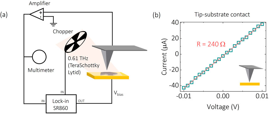
Figure 1. (a) Sketch of the THz-pcAFM setup. A multimeter (HP34401A) measures the current flowing between the AFM tip and the sample. A lock-in amplifier (SR860) detects the photo-induced current by demodulating the DC current signal with respect to the reference frequency from the optical chopper. (b) Electrical resistance of the setup with the platinum probe in direct contact with the gold substrate.
The setup is capable of measuring current transport and, simultaneously, the photo-induced transport from nanoscale objects, thanks to the capability of the AFM to place the probe with nanometric accuracy. Since the AFM probe is movable, it offers the possibility to probe a device by continuously changing its channel length or geometry in general.
3 Experimental results
3.1 THz photo-response
We investigate the THz photo-response of nanometric-thick graphite flakes. The blueish curves in Figures 2a,b show the I-V characteristics of two graphite flakes of 14 to 4 nm in thickness, corresponding to 30 to 10 carbon-atom layers. The conductive AFM probe is kept at a fixed position on the flake. The behavior is slightly superlinear, which is a signature of a potential energy barrier for carriers in the tunneling process between platinum tip and the few-layer graphene. Thin layers of graphite and a metal typically form a low-resistivity ohmic contact Robinson et al. (2011); Xia et al. (2011); Lee et al. (2008), with a negligible potential barrier. In particular, if the work function of the graphene and the metal are different, a significant charge transfer occurs Giovannetti et al. (2008), facilitating the good electrical contact. In our case, the nanometric size of the contact given by the tip radius of the AFM probe makes the electric contact very sensitive to local defects, charge puddles, and contaminants on the sample surface. A small defect density at the nanojunction can easily induce the formation of a small potential barrier. This is especially true in AFM imaging in ambient conditions, where various types of nanometric organic and inorganic contaminants can be attached to the sample and the tip Rozhok et al. (2004). The tunneling barrier from the graphite flake to the tip dominates the I-V characteristic of the circuit. At higher applied voltages, the carriers can overcome the small potential barrier between metal-graphene nanojunction, leading to an increase in the conductivity and a superlinear behavior.
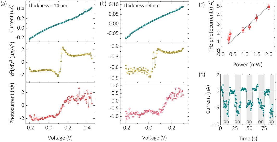
Figure 2. Current (blueish, top-panel), second derivative of the current (dark yellow, central panel), and THz-induced current (red, bottom panel) dependence on the applied bias for a 14 nm-thick (a) and a 4 nm-thick (b) graphite flakes. The DC current shows a superlinear behavior, while the THz-induced current saturates at large applied biases (c) THz power dependence of the photo-induced current under zero applied voltage. (d) DC current under zero applied bias by switching on and off mechanically the THz beam. The THz beam induces a negative DC current under zero bias applied.
The red curves in Figures 2a,b show the voltage dependence of the THz photo-induced current, measured with a lockin amplifier, simultaneously to the cAFM measurements. We observe a THz-induced current signal at zero applied bias. This may be given both by the photo-thermoelectric effect and by THz rectification at the asymmetric AFM probe-graphite-gold junction Vicarelli et al. (2012); Bianco et al. (2015). In various previous works in the literature, it has been shown that the photo-thermoelectric effect in graphene is particularly strong Vicarelli et al. (2012). To get a quantitative estimate of the photo-thermoelectric current, we use the following approximate formula:
By applying a bias voltage, we observe a nonlinear change of the photo-response that cannot be ascribed to the photo-thermoelectric effect. The photo-induced current shows a sharp positive slope at voltages close to 0.15 V and saturates at high applied voltages, both negative and positive. We rule out bolometric effect of graphite as the origin of the nonlinear dependence of the photo-induced current because the series resistance of graphite is very small given the nanometric thickness of the flake and the vertical transport through it. Rather, the resistance is dominated by the platinum-graphite nanojunction. In Figure 2 we report the second derivative of the I-V characteristics (see the Supplementary Material for further details). This quantity is proportional to the current due to THz-induced rectification Schlecht et al. (2019). As can be clearly seen from the figure, there is a good qualitative agreement between the
Finally, we mention the role of the geometric nanometric junction. In fact, as recently studied in graphene Zhu et al. (2013), our system can behave as a geometric diode where the nanometric platinum tip is the contact point, in contrast to the large gold substrate-graphene interface which acts as a counter-electrode. This represents a possible alternative explanation of the rectifying properties manifested by our sample.
3.2 THz nano-imaging
We demonstrate the scanning capability of the setup by measuring AFM topography, cAFM, and THz-pcAFM maps (Figure 3) simultaneously. Figure 3a shows the AFM topography of the few-layer graphene flakes and Figure 3b shows a zoom-in in the 1
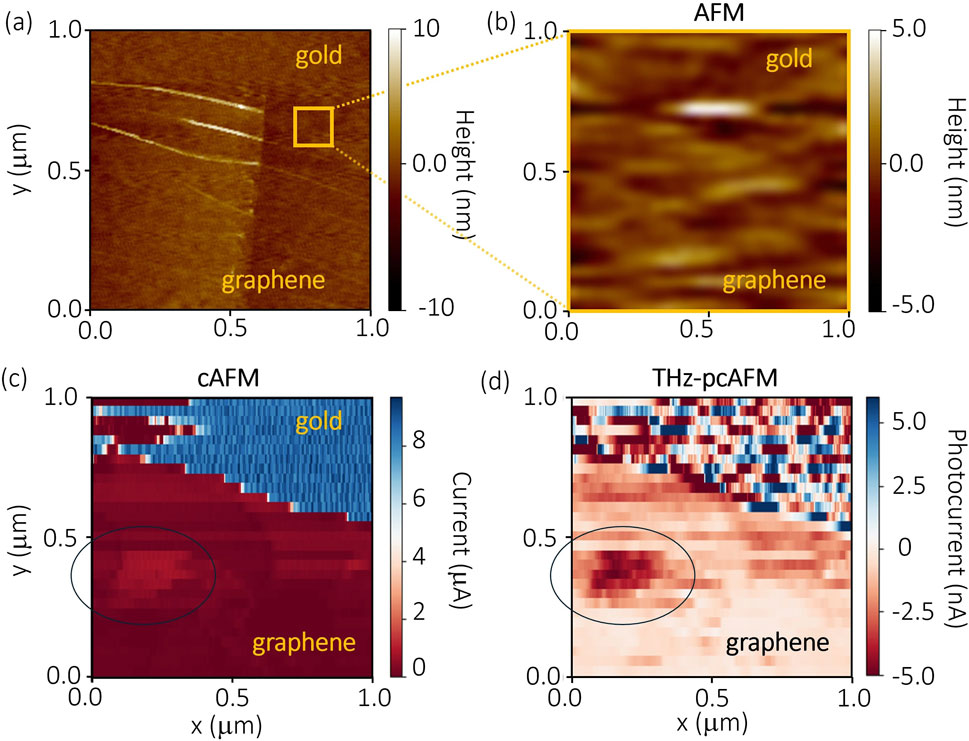
Figure 3. (a) AFM image of the few-layer graphene flake on gold. (b) Zoom-in on the sample region that we probe with cAFM (c) and THz-pcAFM (d). The circles in (c,d) highlight the region of the sample where we observe a charge puddle.
We also note that during the AFM raster scan of the sample, sometimes the electrical contact between the conductive AFM tip and the sample is lost, as it can be observed on the top left corner of Figures 3c,d. The instability of the electrical contact is the main limitation of this technique, a problem discussed in the literature for cAFM Jiang et al. (2019). A critical feature for the stability of the electrical contact is the cleanliness of the sample. In our case, to avoid contaminants on the sample, we use ultra-flat gold freshly stripped from the template as substrate. The graphite flakes are obtained from a chemical vapor deposition-grown crystal. After peeling off a top layer of the graphite via mechanical exfoliation, the crystal is mechanically pressed on the gold without the use of tape or any other polymer. These leaves clean and flat graphite flakes of different thicknesses.
Interestingly, both the cAFM and the THz photo-induced current map show a strong increase of the current/photocurrent in a small region of the few-layer graphene flake, while the rest of the flake has a rather homogeneous current and THz photo-response. The area is about 150 nm wide, which is a dimension that is smaller than the diffraction limit of visible lasers. Techniques such as Raman spectroscopy that we used to probe the sample, typically average over these regions. We interpret this observation as a consequence of a charge puddle in the few-layer graphene flake Martin et al. (2008); Samaddar et al. (2016). Since we do not observe any clear corrugation in the AFM topography, the charge puddle is likely induced by charged impurities between the few-layer graphene and the gold substrate Zhang et al. (2009). It is fundamental to remark that the charge puddle results in an increase of both the DC current and photocurrent absolute signal. This means that the observed increase cannot be solely due to the photo-thermoelectric effect. In fact, a change in the Seebeck coefficient, which depends nonlinearly on the local charge density Castilla et al. (2019); Duan et al. (2016), would affect the photocurrent but not the DC current. As a consequence of this observation, we hypothesize that the main role of the charge puddle is to increase the number of available charges that can tunnel between the tip and the sample. Quantifying charge density from our measurements would be of crucial importance for the future refinement of the THz-pcAFM technique. However, for this kind of estimation it is essential to develop a precise quantitative model to describe the photocurrent. This quantitative analysis goes beyond the scope of this work, and would be indeed particularly tough without knowing some key parameters, such as the precise mechanisms governing the photo-induced current signal and the evaluation of the graphite flakes intrinsic doping level.
The observation of charge puddles in graphene has been obtained by means of scanning tunneling microscopy (STM) Zhang et al. (2009), single-electron transistor (SET) microscopy Martin et al. (2008) and other scanning probe microscopy techniques Zhao et al. (2021). In our experimental, the spatial resolution of our experimental setup is given mostly by the tip apex (20 nm of radius), enlarged by the current pathways that are not solely vertical. As a consequence, we are limited to observing charge puddles of about hundred of nanometers in size, different from what has been observed in STM experiments Zhang et al. (2009) where smaller charge puddles have been observed. Another important distinction lies in the sample cleanliness. In the STM and SET experiments performed in the aforementioned works, charge puddles are observed in an ultra-high vacuum chamber, after a proper thermal annealing of the sample. By doing so, the amount of adsorbates is significantly reduced with respect to our ambient temperature and pressure conditions. This may lead to significant changes in the origin of the puddles that in our case may be due to deep potential traps caused by adsorbates. Finally, while both SET and STM techniques involve a negligible flow of current between tip and sample, our THz-pcAFM setup relies on a good electrical contact. This implies a significant amount of charge transfer, and hence a change of the local Fermi energy of few-layer graphene depending on the relative work functions of platinum and graphite Giovannetti et al. (2008). In this sense, our approach is more perturbative and less accurate to quantify the charge density in the puddles.
4 Conclusion
In conclusion, we have coupled a focused Gaussian beam at 0.61 THz to a conductive AFM setup employing platinum probes that also act as THz nanoantennas. The resulting system acquires THz photocurrent maps at the nanoscale, thus measuring nanometer-resolved surface quality maps of 2D materials. As an example, we have mapped charge puddles in a few-layer graphene flake, and we show that the nanojunctions between platinum and few-layer graphene flakes form an electric potential barrier with THz rectification capabilities, both at zero DC bias and with a DC bias voltage applied to the AFM probe. This rectification capability of the metal-graphene junctions can be exploited to characterize and develop light detectors in the THz and infrared ranges.
Data availability statement
The raw data supporting the conclusions of this article will be made available by the authors, without undue reservation.
Author contributions
EF: Data curation, Validation, Methodology, Investigation, Software, Writing – review and editing, Visualization, Writing – original draft, Formal Analysis. FB: Validation, Writing – review and editing, Investigation. MT: Methodology, Validation, Writing – review and editing. LB: Resources, Funding acquisition, Validation, Writing – review and editing, Investigation, Methodology. MO: Funding acquisition, Investigation, Conceptualization, Resources, Writing – original draft, Validation, Writing – review and editing, Supervision. VG: Conceptualization, Validation, Methodology, Supervision, Investigation, Writing – review and editing. TV: Supervision, Methodology, Investigation, Conceptualization, Writing – review and editing, Data curation, Software, Formal Analysis, Writing – original draft, Visualization.
Funding
The author(s) declare that financial support was received for the research and/or publication of this article. MO, VG and TV acknowledge funding by the European Innovation Council (NEHO 101046329). Views and opinions expressed are however those of the authors only and do not necessarily reflect those of the European Union or EIC. Neither the European Union nor the granting authority can be held responsible for them.
Conflict of interest
The authors declare that the research was conducted in the absence of any commercial or financial relationships that could be construed as a potential conflict of interest.
Generative AI statement
The author(s) declare that no Generative AI was used in the creation of this manuscript.
Publisher’s note
All claims expressed in this article are solely those of the authors and do not necessarily represent those of their affiliated organizations, or those of the publisher, the editors and the reviewers. Any product that may be evaluated in this article, or claim that may be made by its manufacturer, is not guaranteed or endorsed by the publisher.
Supplementary material
The Supplementary Material for this article can be found online at: https://www.frontiersin.org/articles/10.3389/fphot.2025.1638350/full#supplementary-material
References
Alonso-González, P., Nikitin, A. Y., Gao, Y., Woessner, A., Lundeberg, M. B., Principi, A., et al. (2017). Acoustic terahertz graphene plasmons revealed by photocurrent nanoscopy. Nat. Nanotechnol. 12, 31–35. doi:10.1038/nnano.2016.185
An, S., Park, H., and Kim, M. (2023). Recent advances in single crystal narrow band-gap semiconductor nanomembranes and their flexible optoelectronic device applications: ge, gesn, ingaas, and 2d materials. J. Mater. Chem. C 11, 2430–2448. doi:10.1039/d2tc05041b
Bianco, F., Perenzoni, D., Convertino, D., De Bonis, S., Spirito, D., Perenzoni, M., et al. (2015). Terahertz detection by epitaxial-graphene field-effect-transistors on silicon carbide. Appl. Phys. Lett. 107. doi:10.1063/1.4932091
Cao, L., Park, J.-S., Fan, P., Clemens, B., and Brongersma, M. L. (2010). Resonant germanium nanoantenna photodetectors. Nano Lett. 10, 1229–1233. doi:10.1021/nl9037278
Casini, R., Di Gaspare, A., Giovine, E., Notargiacomo, A., Ortolani, M., and Foglietti, V. (2011). Three-dimensional shaping of sub-micron gaas schottky junctions for zero-bias terahertz rectification. Appl. Phys. Lett. 99. doi:10.1063/1.3672439
Castilla, S., Terrés, B., Autore, M., Viti, L., Li, J., Nikitin, A. Y., et al. (2019). Fast and sensitive terahertz detection using an antenna-integrated graphene pn junction. Nano Lett. 19, 2765–2773. doi:10.1021/acs.nanolett.8b04171
Citroni, R., Di Paolo, F., and Livreri, P. (2022). Progress in thz rectifier technology: research and perspectives. Nanomaterials 12, 2479. doi:10.3390/nano12142479
Cocker, T., Jelic, V., Hillenbrand, R., and Hegmann, F. (2021). Nanoscale terahertz scanning probe microscopy. Nat. photonics 15, 558–569. doi:10.1038/s41566-021-00835-6
Cocker, T. L., Jelic, V., Gupta, M., Molesky, S. J., Burgess, J. A., Reyes, G. D. L., et al. (2013). An ultrafast terahertz scanning tunnelling microscope. Nat. Photonics 7, 620–625. doi:10.1038/nphoton.2013.151
Dong, Y., Sun, Z., Phinney, I., Sun, D., Andersen, T., Xiong, L., et al. (2025). Current-driven nonequilibrium electrodynamics in graphene revealed by nano-infrared imaging. Nat. Commun. 16, 3861. doi:10.1038/s41467-025-58953-6
Duan, J., Wang, X., Lai, X., Li, G., Watanabe, K., Taniguchi, T., et al. (2016). High thermoelectricpower factor in graphene/hbn devices. Proc. Natl. Acad. Sci. 113, 14272–14276. doi:10.1073/pnas.1615913113
Giovannetti, G., Khomyakov, P. A., Brocks, G., Karpan, V. v., van den Brink, J., and Kelly, P. J. (2008). Doping graphene with metal contacts. Phys. Rev. Lett. 101, 026803. doi:10.1103/physrevlett.101.026803
Goossens, A., Calado, V., Barreiro, A., Watanabe, K., Taniguchi, T., and Vandersypen, L. (2012). Mechanical cleaning of graphene. Appl. Phys. Lett. 100. doi:10.1063/1.3685504
Guo, X., Bertling, K., Donose, B. C., Brünig, M., Cernescu, A., Govyadinov, A. A., et al. (2024). Terahertz nanoscopy: advances, challenges, and the road ahead. Appl. Phys. Rev. 11, 021306. doi:10.1063/5.0189061
Hillenbrand, R., Abate, Y., Liu, M., Chen, X., and Basov, D. (2025). Visible-to-thz near-field nanoscopy. Nat. Rev. Mater. 10, 285–310. doi:10.1038/s41578-024-00761-3
Intze, A., Temperini, M. E., Gregori, G., Verde, F., Ortolani, M., and Giliberti, V. (2024). Effect of 0.6 thz continuous-wave irradiation on pathologically relevant protein aggregates. IEEE Trans. Terahertz Sci. Technol. 14, 652–660. doi:10.1109/tthz.2024.3435397
Jiang, L., Weber, J., Puglisi, F. M., Pavan, P., Larcher, L., Frammelsberger, W., et al. (2019). Understanding current instabilities in conductive atomic force microscopy. Materials 12, 459. doi:10.3390/ma12030459
Lee, E. J., Balasubramanian, K., Weitz, R. T., Burghard, M., and Kern, K. (2008). Contact and edge effects in graphene devices. Nat. Nanotechnol. 3, 486–490. doi:10.1038/nnano.2008.172
Leinß, S., Kampfrath, T., Volkmann, K. v., Wolf, M., Steiner, J. T., Kira, M., et al. (2008). Terahertz coherent control of optically dark paraexcitons in cu2o. Phys. Rev. Lett. 101, 246401. doi:10.1103/physrevlett.101.246401
Liu, C.-H., Chang, Y.-C., Norris, T. B., and Zhong, Z. (2014). Graphene photodetectors with ultra-broadband and high responsivity at room temperature. Nat. Nanotechnol. 9, 273–278. doi:10.1038/nnano.2014.31
Martin, J., Akerman, N., Ulbricht, G., Lohmann, T., Smet, J. v., Von Klitzing, K., et al. (2008). Observation of electron–hole puddles in graphene using a scanning single-electron transistor. Nat. Phys. 4, 144–148. doi:10.1038/nphys781
Mittendorff, M., Winnerl, S., Kamann, J., Eroms, J., Weiss, D., Schneider, H., et al. (2013). Ultrafast graphene-based broadband thz detector. Appl. Phys. Lett. 103. doi:10.1063/1.4813621
Mittendorff, M., Winnerl, S., and Murphy, T. E. (2021). 2d thz optoelectronics. Adv. Opt. Mater. 9, 2001500. doi:10.1002/adom.202001500
Robinson, J. A., LaBella, M., Zhu, M., Hollander, M., Kasarda, R., Hughes, Z., et al. (2011). Contacting graphene. Appl. Phys. Lett. 98. doi:10.1063/1.3549183
Rozhok, S., Sun, P., Piner, R., Lieberman, M., and Mirkin, C. A. (2004). Afm study of water meniscus formation between an afm tip and nacl substrate. J. Phys. Chem. B 108, 7814–7819. doi:10.1021/jp0401269
Samaddar, S., Yudhistira, I., Adam, S., Courtois, H., and Winkelmann, C. (2016). Charge puddles in graphene near the dirac point. Phys. Rev. Lett. 116, 126804. doi:10.1103/physrevlett.116.126804
Schwartz, J. J., Jakob, D. S., and Centrone, A. (2022). A guide to nanoscale ir spectroscopy: resonance enhanced transduction in contact and tapping mode afm-ir. Chem. Soc. Rev. 51, 5248–5267. doi:10.1039/d2cs00095d
Temperini, M. E., Polito, R., Venanzi, T., Baldassarre, L., Hu, H., Ciracì, C., et al. (2024). An infrared nanospectroscopy technique for the study of electric-field-induced molecular dynamics. Nano Lett. 24, 9808–9815. doi:10.1021/acs.nanolett.4c01387
Venanzi, T., Cuccu, M., Perea-Causin, R., Sun, X., Brem, S., Erkensten, D., et al. (2024a). Ultrafast switching of trions in 2d materials by terahertz photons. Nat. Photonics 18, 1344–1349. doi:10.1038/s41566-024-01512-0
Venanzi, T., Giliberti, V., Temperini, M., Sotgiu, S., Polito, R., Mattioli, F., et al. (2023). Mid-infrared photocurrent nano-spectroscopy exploiting the thermoelectric effect in graphene. Appl. Phys. Lett. 123. doi:10.1063/5.0162631
Venanzi, T., Temperini, M. E., Baldassarre, L., Ortolani, M., and Giliberti, V. (2024b). Mid-infrared assisted transport at the nano-junction between graphene and a doped-diamond scanning probe. Photonics Nanostructures-Fundamentals Appl. 58, 101243. doi:10.1016/j.photonics.2024.101243
Vicarelli, L., Vitiello, M., Coquillat, D., Lombardo, A., Ferrari, A. C., Knap, W., et al. (2012). Graphene field-effect transistors as room-temperature terahertz detectors. Nat. Mater. 11, 865–871. doi:10.1038/nmat3417
Xia, F., Perebeinos, V., Lin, Y.-m., Wu, Y., and Avouris, P. (2011). The origins and limits of metal–graphene junction resistance. Nat. Nanotechnol. 6, 179–184. doi:10.1038/nnano.2011.6
Yi, S.-G., Kim, S. H., Park, S., Oh, D., Choi, H. Y., Lee, N., et al. (2016). Mo1−xwxse2-based schottky junction photovoltaic cells. ACS Appl. Mater. and interfaces 8, 33811–33820. doi:10.1021/acsami.6b11768
Zhang, Y., Brar, V. W., Girit, C., Zettl, A., and Crommie, M. F. (2009). Origin of spatial charge inhomogeneity in graphene. Nat. Phys. 5, 722–726. doi:10.1038/nphys1365
Zhao, M., Kim, D., Lee, Y., Ling, N., Zheng, S., Lee, Y. H., et al. (2021). Harnessing thermoelectric puddles via the stacking order and electronic screening in graphene. ACS nano 15, 5397–5404. doi:10.1021/acsnano.1c00030
Keywords: AFM, THz, photocurrent, THz nanoimaging, graphene
Citation: Fragomeni E, Berkmann F, Temperini ME, Baldassarre L, Ortolani M, Giliberti V and Venanzi T (2025) Terahertz photoconductive atomic force microscopy of few-layer graphene flakes. Front. Photonics 6:1638350. doi: 10.3389/fphot.2025.1638350
Received: 30 May 2025; Accepted: 25 July 2025;
Published: 06 August 2025.
Edited by:
Chiara Schiattarella, Nanoscience Institute, ItalyReviewed by:
Andres De Luna, National Autonomous University of Mexico, MexicoLeonardo Viti, Istituto Nanoscienze, Italy
Copyright © 2025 Fragomeni, Berkmann, Temperini, Baldassarre, Ortolani, Giliberti and Venanzi. This is an open-access article distributed under the terms of the Creative Commons Attribution License (CC BY). The use, distribution or reproduction in other forums is permitted, provided the original author(s) and the copyright owner(s) are credited and that the original publication in this journal is cited, in accordance with accepted academic practice. No use, distribution or reproduction is permitted which does not comply with these terms.
*Correspondence: Tommaso Venanzi, dG9tbWFzby52ZW5hbnppQGlpdC5pdA==