 Antonio Abate*
Introduction
In 1638, the Italian astronomer Galileo Galilei designed one of the first experiments attempting to measure the speed of light (Foschi and Leone, 2009). Although the test was not conclusive, it reinforced the hypothesis that light could have a finite speed. The speed limit was one of the key steps toward understanding the elusive nature of light and the complex phenomena that surrounds light-matter interaction. Much later, it was demonstrated that when light (and any electromagnetic radiation in general) interacts with matter, it might induce a flow of electrons. Symmetrically, a flow of electrons within matter might generate electromagnetic radiation.
We call optoelectronics “the study and the application of the phenomena, materials, and devices involved with the interaction between electrons within a material or a device and the absorption or emission of electromagnetic radiation from the same” (Koch, 2014).
Optoelectronic is essential in modern life, and it will become increasingly more important in future because technological development is relying more and more on the diffusion of devices that source, detect, and control electromagnetic radiation. X-ray, ultraviolet, visible, and infrared light optoelectronics are the most relevant. They are involved in a large number of applications in many relevant fields of technological development, including but not limited to Energy, Medicine, Architecture, Communication, Robotics, Transport, Security, and Entertainment. Below we report some examples of applications representative of the fields listed above (Figure 1).
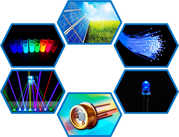
FIGURE 1. Schematic showing pictures of a few examples of optoelectronic devices.
Energy
The demand for electricity has been steadily increasing since we started to monitor it. The consumption of fossil fuels to meet the requirement for electricity is being progressively abandoned as people turn toward new and renewable sources of energy. Among renewables, photovoltaic energy production is one of the most promising since it is capable of meeting a significant share of the worldwide energy demands in the next few decades. Here, optoelectronics is playing a fundamental role. The research and development of more efficient photovoltaic solar cells identified several new materials that enabled devices capable of converting sunlight into electric power with an unprecedented power conversion efficiency and at a fractional cost of the state-of-the-art technologies (Polman et al., 2016). We do expect an exponential increase of public and private investment in photovoltaics, both toward fundamental research and toward the development of products for large-scale production.
Together with light-harvesting for energy, light generation from low-energy consumption is a consolidated strategy to mitigate the increasing demand. Over the last few years, we assisted in the revolutionary design of light-emitting diodes (LEDs) that replaced incandescent bulbs to generate light. LEDs are a dynamic field of research that is experimenting with the application of new materials to prepare more efficient and cost-effective LEDs.
Medicine
Wearable and implantable devices are spreading massively in healthcare for monitoring, diagnosis, and therapy. We are used to multi-component devices, such as wearable fitness watches and implantable cardiac monitors, that can read and transmit, for example, heart rate, temperature and, with the most advanced versions, the sweat composition for monitoring diabetes. Here, optoelectronics can offer significant progress toward integrating the functionality of a multi-component device in a disposable sticker for healthcare monitoring, diagnosis, and therapy. Integrating display, sensor, and energy supply functionalities within the same sticker calls for flexible and stretchable thin optoelectronics.
Furthermore, implantable systems require biocompatibility and resistance in a biological environment. For example, edible devices would allow for monitoring of a wide range of health diseases, but they need to be compatible with the tissue they are going to be in contact with. One example of implantable systems is the artificial retina (Ghezzi et al., 2011). Loss of vision due to retinal degeneration affects a non-negligible part of the worldwide population. Retinal degradation originates mainly from diseases and aging. Different approaches, including purely biological approaches, such as in vitro or in vivo regeneration, are currently being explored. An optoelectronic approach aiming to create an artificial retina that is capable of converting incoming light into electrical signals and transmitting them to the neurons is collecting more and more interest among research institutes and private companies.
Architecture
The construction of new commercial and residential buildings must consider energy efficiency as one of the main guiding principles during planning. Optoelectronics can play an important role in increasing building energy efficiency. Building-integrated photovoltaics is a well-established approach (Biyik et al., 2017). Here, the architects are made to consider aesthetic aspects. Thus, the application has to consider, for example, the possibility of creating a device colored a specific way and to integrate them with other architectonic elements. Developing flexible solar cells that can be modeled on different surfaces allow for coating of the entire external surface of the building. Besides producing energy, saving energy by managing indoor illumination with smart windows is also considered very useful. Smart windows can be prepared with optoelectronics devices that can modulate the light entering buildings (Ke et al., 2019). The current technologies are rather expensive and thus not widespread. New optoelectronics solutions are highly desired in this field.
Communication
Internet of things is revolutionizing our lives in many fields and from multiple aspects (Nauman et al., 2020). The concept of enabling devices to communicate has been considered since the computer era. However, it has only recently become effectively applicable, and it will unavoidably invade our life soon. Examples of application fields are smart homes, elder care, health care, environmental monitoring, manufacturing, and many others. Regardless of the application, the optoelectronic can deliver an infinite number of solutions to support the development of Internet of things. One example is powering indoor and outdoor devices to make them independent from the electric network and thus portable.
Robotics
The idea of having machines that can help and assist humans in their day-to-day lives is an old vision that is becoming real. Robots are primarily used for manufacturing but are becoming more and more important in medicine, elder care, and health care. The more complex the task the robot has to accomplish, the higher the level of interaction the robot needs with the surrounding environment. Sensors are essential to make the robot aware of what is going on around it. Here, optoelectronics is critical. When we talk about robots, we should not think about a human-like machine but rather a miniaturized system that accomplishes a specific function. Thus, sensors need to be adapted to the task the robot has to perform, and they should be as low-energy consuming as possible or, ideally, self-powering.
Transport
Self-driving cars are more than a promise for the future of transportation. Many companies are actively investing in developing their algorithms and prototypes. The functioning of these vehicles relies on the analysis of the information collected by a myriad of sensors. The three primary self-driving cars sensors are camera, radar, and lidar, which are different examples of optoelectronics. The cameras collect the images that are analyzed by the software to identify obstacles. Radar sensors, similar to those mounted on aircrafts and ships, can support the camera vision in case of low visibility. A lidar—a sensor that measures the distance by pulsed lasers—can recreate a 3D picture of the environment in almost any condition of visibility (Wu et al., 2020). Such a sensor is considered fundamental for self-driving cars. However, they are far more expensive than cameras and radar, and they still have a limited range of detection around the vehicle.
Entertainment
Ultra-high-definition screens for televisions and virtual reality systems are two pillars of entertainment. Here the application of optoelectronics is driven mainly by private companies that finance the development of more advanced products. However, we would not be surprised if further advancements will come from fundamental research that will apply optoelectronics to entertainment.
Optoelectronics of Tomorrow
We believe that optoelectronics will be an essential technological accelerator for the coming decades. We are collecting information on materials and devices to unlock unprecedented technological advancements. Nevertheless, we have to respect the environment and the resources that future generations will inherit. A concept like renewable materials, self-powering devices, and circular lifecycles are mandatory while designing future technologies.
Sustainable Materials
Future optoelectronics will rely on the most recent advancement in new materials. While the last century saw the success of silicon and other inorganics, the future will see the ingress of organic and hybrid organic-inorganic materials into optoelectronics. We already have a large number of examples in different fields of applications. Organic is not necessarily going to replace inorganic, nor do we believe that organic will be cheaper than inorganic. We do find that the use of organic and hybrid materials will unlock new opportunities. One of the most recent pieces of evidence is the use of hybrid halide perovskite in photovoltaic solar cells (Correa-Baena et al., 2017). Perovskite is unlikely going to replace the silicon photovoltaic market. Still, it is reasonable to predict that a combination of perovskite and silicon in tandem devices will deliver the next generation of solar cells. The primary driving principle in the exploration and selection of new materials is taking care when using earth-abundant and non-toxic elements that can be recycled with inexpensive and clean processing.
Self-Powering Devices
Optoelectronics need electric energy. As the number of optoelectronic devices employed in any aspect of our lives is increasing exponentially, we should expect that the demand for batteries grows too. A possible solution to reduce the need for batteries is to push for self-powering optoelectronics. One of the approaches to deliver self-powering devices is integrating solar cells within the device. Indoor photovoltaic solar cells are one example of providing self-powering for wireless indoor optoelectronics for home automation systems that control lighting, climate, entertainment systems, and appliances (Mathews et al., 2019). However, photovoltaic powering is not always possible. Alternative solutions designed for this specific application are thus in high demand and will be a challenge for the future.
Circular Life Cycle
The design of a new technology cannot ignore the lifecycle of the design, accounting for the environmental impact across all stages of raw material extraction, material processing, manufacturing, use, and end-of-life. A life cycle approach makes it more challenging to identify new technological solutions, and it implies a multidisciplinary method for developing the optoelectronics of the future.
Scientific and Technological Challenges
The paradigm of future optoelectronics is to deliver high performing devices that have a low environmental impact, i.e., make use of non-toxic elements and green manufacturing processes. This challenge makes the research and development of new technologies far more complicated than in the past. A multidisciplinary approach encompassing expertize from both basic science and process engineering seems necessary.
A significant boost to the field could come from the application of machine learning to specific tasks. One of the most productive areas of use is the screening of new materials that match the renewable criteria and circular lifecycle mentioned above. Here the application of machine learning can significantly speed up the discovery and the synthesis of a new class of materials for optoelectronics. For example, the recent rise of interest for halide perovskites demonstrated that the entire library made up of thousands of potential optoelectronic materials had so far been ignored. Exploring all the possibilities that halide perovskites can offer is nearly impossible when following a simple experimental approach. The application of machine learning seems almost necessary to fully exploit this new class of materials.
Similarly, many other material concepts are there waiting. However, despite the rapid development, many aspects of merging machine learning with material science remain only partially explored and challenging. Most of the work has been, in fact, devoted to developing machine learning architecture to generate predictors that connect physical structures to their properties. Another very fruitful research line was the use of generative methods to “create” new in-silico materials directly. Far less work has been devoted to applying machine learning directly to the synthesis, fabrication, and deposition processes of materials and devices. We do believe that taking the challenge of machine learning applied to materials and devices for optoelectronics will open up new and unexpected opportunities.
Automated high-throughput platforms for preparing and testing new materials and devices can be designed and implemented, making use of robotics. As many technologies rely on the identification of new materials and processing that is compatible with the specific application, the use of robots for fast screening is becoming of increasing interest in many fields of research and development. For example, several technologies currently in use are manufactured using toxic solvents. One can think of replacing toxic solvents with an automated screening of green alternatives for a specific application (Gu et al., 2020). This approach, which is now in use for simple tasks, will be developed for more complicated procedures.
Storing data in large databanks is already being done for several activities of our life. Taking advantage of these databases to extract information is what we are learning to do. The application of big data analysis to the development of new optoelectronics is a potential new compelling scenario. We expect that the use of machine learning in big data will allow for an entirely new approach to the research of new technological solutions. Ideally, new materials and device concepts will be predicted similarly to what theoretical physicists have been making with subatomic particles in the past.
Overview
A future made of autonomous transporting vehicles, intelligent robots, and human and building integrated devices relies on advancing the basic science and the technology behind the application of optoelectronics. New material and device concepts will result in the optoelectronics necessary for autonomous vehicles to move around safely and for robots to interact deeply with the surrounding environment. Implantable and wearable optoelectronics will massively impact health and elder care. Buildings will become more and more smart, reducing the consumption of energy and enhancing comfort indoors. There any many other fields which will benefit from the joint effort of academic and industrial research toward a sustainable future.
Conflict of Interest
The author declares that the research was conducted in the absence of any commercial or financial relationships that could be construed as a potential conflict of interest.
References
Biyik, E., Araz, M., Hepbasli, A., Shahrestani, M., Yao, R., Shao, L., et al. (2017). A key review of building integrated photovoltaic (BIPV) systems. Eng. Sci. Technol. Int. J. 20 (3), 833–858. doi:10.1016/j.jestch.2017.01.009
Correa-Baena, J.-P., Saliba, M., Buonassisi, T., Grätzel, M., Abate, A., Tress, W., et al. (2017). Promises and challenges of perovskite solar cells. Science 358 (6364), 739–744. doi:10.1126/science.aam6323
Foschi, R., and Leone, M. (2009). Galileo, measurement of the velocity of light, and the reaction times. Perception 38 (8), 1251–1259. doi:10.1068/p6263
Ghezzi, D., Antognazza, M. R., Maschio, M. D., Lanzarini, E., Benfenati, F., and Lanzani, G. (2011). A hybrid bioorganic interface for neuronal photoactivation. Nat. Commun. 2 (1), 1–7. doi:10.1038/ncomms1164
Gu, E., Tang, X., Langner, S., Duchstein, P., Zhao, Y., Levchuk, I., et al. (2020). Robot-based high-throughput screening of antisolvents for lead halide perovskites. Joule, 1806–1822. doi:10.1016/j.joule.2020.06.013
Ke, Y., Chen, J., Lin, G., Wang, S., Zhou, Y., Yin, J., et al. (2019). Smart windows: electro‐, thermo‐, mechano‐, photochromics, and beyond. Adv. Energy Mater. 9 (39), 1902066. doi:10.1002/aenm.201902066
N. Koch (Editor) (2014). Supramolecular materials for opto-electronics. London, United Kingdom: Royal Society of Chemistry.
Mathews, I., Kantareddy, S. N., Buonassisi, T., and Peters, I. M. (2019). Technology and market perspective for indoor photovoltaic cells. Joule 3 (6), 1415–1426. doi:10.1016/j.joule.2019.03.026
Nauman, A., Qadri, Y. A., Amjad, M., Zikria, Y. B., Afzal, M. K., and Kim, S. W. (2020). Multimedia internet of things: a comprehensive survey. IEEE Access 8, 8202–8250. doi:10.1109/ACCESS.2020.2964280
Polman, A., Knight, M., Garnett, E. C., Ehrler, B., and Sinke, W. C. (2016). Photovoltaic materials: present efficiencies and future challenges. Science 352 (6283), aad4424. doi:10.1126/science.aad4424
Keywords: optoelectronics, solar, light-emitting diode, sensor, energy
Citation: Abate A (2020) Specialty Grand Challenges in Optoelectronics. Front. Electron. 1:579890. doi:10.3389/felec.2020.579890
Received: 03 July 2020; Accepted: 12 August 2020;
Published: 25 August 2020.
Edited by:
Yue Hu, Huazhong University of Science and Technology, ChinaReviewed by:
Claudia Barolo, University of Turin, ItalyPetr Kovaricek, J. Heyrovsky Institute of Physical Chemistry (ASCR), Czechia
Jiangjian Shi, Institute of Physics (CAS), China
Copyright © 2020 Abate. This is an open-access article distributed under the terms of the Creative Commons Attribution License (CC BY). The use, distribution or reproduction in other forums is permitted, provided the original author(s) and the copyright owner(s) are credited and that the original publication in this journal is cited, in accordance with accepted academic practice. No use, distribution or reproduction is permitted which does not comply with these terms.
*Correspondence: Antonio Abate, YW50b25pby5hYmF0ZUBoZWxtaG9sdHotYmVybGluLmRl