 Xintai Wang1
 Maksim Kuznetcov1Wenfeng Jiang1Zhongyu Tang1Zhangchenyu Wei1Aili Zhang1Naixu Wei1Xiaoying Li2*
- 12D Material Lab, Zhejiang Mashang GM2D Research Institute, Wenzhou, China
- 2College of Environmental Science and Engineering, Dalian Maritime University, Dalian, China
This review investigates the revolutionary potential of printed RFID technology in enabling next-generation IoT systems through sustainable manufacturing. The analysis systematically evaluates emerging conductive ink formulations, including metallic nanoparticles, carbon-based nanomaterials, MXenes, and hybrid composites, while assessing their performance trade-offs in electrical conductivity, environmental stability, and printing compatibility. Fundamental design strategies for high-performance antennas are examined, focusing on impedance matching optimization, radiation pattern control, and substrate-material synergy. Advances in printing methodologies such as inkjet deposition, screen printing, and direct ink writing are comparatively analyzed, with particular attention to the trade-off between performance and efficiency in high-resolution patterning versus industrial-scale production. Technical bottlenecks restricting commercial application are critically evaluated, emphasizing material property limitations and performance variations induced by the printing process. Finally, the study proposes three synergistic innovation pathways: intelligent material discovery through machine learning algorithms, multi-parameter simulation-guided antenna design, and hybrid manufacturing integrating multiple printing technologies. These integrated approaches aim to accelerate the transition from prototype development to industrial deployment of printed RFID systems. This comprehensive assessment provides actionable insights for advancing eco-friendly, mass-producible RFID solutions that meet the escalating demands of ubiquitous IoT connectivity across various smart environments.
1 Introduction
Radio Frequency Identification (RFID) technology has evolved into a versatile solution for contactless identification in diverse industrial sectors (Khan et al., 2024), including logistics (Yu and Wang, 2021; Werthmann et al., 2017), healthcare (Amendola et al., 2014; Sani et al., 2010), and supply chain management (Shariq et al., 2021). Unlike conventional optical systems like barcodes or QR codes, RFID offers key advantages: automated data capture without manual intervention, extended operational ranges exceeding 10 m for passive tags, and simultaneous recognition of multiple tags without line-of-sight requirements (Varriale et al., 2021; Ondemir et al., 2012; Roy et al., 2010). These characteristics make RFID fundamental to perception layers in the Internet of Things (IoT) ecosystem, where distributed sensing and traceability generate critical datasets for advanced analytics. Recent sensor integration progress extends RFID functionality beyond basic identification, enabling real-time monitoring of essential environmental parameters such as temperature fluctuations (Shafiq et al., 2019; Zhou et al., 2024), chemical exposure levels (Jun et al., 2016), and mechanical stress conditions (Ju et al., 2024). This technological integration has opened new application domains in precision environmental monitoring (Kassal et al., 2018), advanced medical diagnostics (Sun et al., 2021), and intelligent packaging systems with embedded quality indicators (Wang G. et al., 2019).
Antennas are the essential electromagnetic interface for reliable radio frequency signal transmission in RFID systems. The antenna architecture directly influences critical performance metrics: operational range across diverse environmental conditions, data transmission speed in high-density tag deployment scenarios, and resilience to electromagnetic interference. Although industrial manufacturing primarily relies on etched aluminum deposition processes, additive printed electronics has emerged as a sustainable fabrication alternative (Zhang and Cui, 2017; Subramanian et al., 2005; Rizwan et al., 2017; Kavcic et al., 2014; Fathi et al., 2021). This approach enables direct deposition of precision-patterned antennas onto various substrates—including flexible textiles, curved glass, and multilayer packaging materials—while eliminating the need for traditional photolithography and chemical etching. The additive method dramatically reduces material waste and hazardous chemical byproducts, concurrently lowering production costs—advantages that strongly align with global sustainability goals in electronics manufacturing.
Developing high-performance printed RFID systems requires the coordinated development of three interdependent domains: conductive ink formulation, antenna geometric design, and printing process optimization. Conductive inks—typically composed of metallic nanoparticles, carbon-based materials, or hybrid composites—demand careful balancing of electrical conductivity, environmental stability, and cost-efficiency. Simultaneously, antenna miniaturization for compact tags must address fundamental trade-offs between radiation efficiency and operational bandwidth, particularly at UHF frequencies. Printing techniques such as inkjet and screen printing require optimization across pattern resolution, manufacturing throughput, and compatibility with flexible or textured substrates. Although recent advances in nano-engineered materials and additive manufacturing have alleviated some constraints, the systemic integration of materials, devices, and processes remains challenging for achieving commercial-scale reliability.
Previous studies have often focused on isolated technical aspects of printed RFID systems. Yang et al. (2022) (Yang et al., 2023a) provided a comprehensive overview of conductive ink formulation via combinatorial optimization. Hamidon et al. (2021) (Hamidon et al., 2024) systematically characterized printable materials compatible with RFID-specific printing processes, establishing correlations among substrate properties, fabrication methods, and print quality. Rida et al. (2020) (Rida et al., 2009) developed structured frameworks for evaluating inkjet-printed antennas, demonstrating variations in radiation efficiency across different printed patterns. Nevertheless, these foundational studies typically examined technical elements in isolation rather than investigating their synergistic interactions within integrated architectures.
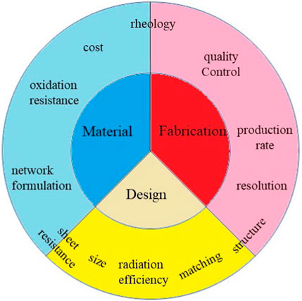
Building upon this background, this review methodically examines cross-disciplinary advancements through three critical perspectives (Figure 1): material innovations in conductive composites (Section 2), topology-optimized antenna architectures (Section 3), and hybrid printing methodologies (Section 4). Finally, we discuss current challenges and emerging opportunities for printed RFID technology, concluding with forward-looking research perspectives (Section 5).
2 Conductive inks
2.1 Basic principles of conductive Ink network formulation
Conductive ink systems form the foundation of printed RFID technology, requiring precise engineering to balance electrical conductivity, manufacturing cost, and fabrication compatibility.
A standard conductive ink formulation comprises four components: conductive fillers, polymeric binders, carrier liquids, and functional additives. Conductive particles or flakes, which serve as the primary conductive fillers, directly determine the electrical performance of the ink. These fillers are dispersed uniformly within organic or aqueous carrier liquids, where specialized additives stabilize colloidal suspensions and modulate rheological behavior to match specific printing methodologies. Following deposition, the ink undergoes solvent evaporation during drying, followed by sintering—a thermal treatment that increases filler concentration until it surpasses the percolation threshold. During this phase, adjacent particles fuse via atomic diffusion, forming a continuous conductive network. Concurrently, polymeric binders immobilize the filler particles, thereby enhancing mechanical stability and minimizing the risk of interfacial delamination.
The selection of filler materials critically determines ink performance metrics. Industrial-scale production predominantly employs two synthesis strategies: bottom-up and top-down approaches. The bottom-up methodology, which involves atomic/molecular assembly, produces fillers with narrow size distributions and high crystallinity, at the expense of higher production costs (Wang Y. et al., 2019). In contrast, the top-down approach utilizes mechanical milling or exfoliation to reduce bulk materials, offering cost advantages but requiring stringent defect control to minimize structural imperfections (Li P. et al., 2024; Claypole et al., 2021). Regardless of the synthesis route, the ultimate conductivity of printed patterns depends on three interdependent factors: (i) the intrinsic conductivity of the filler material, (ii) the morphology of interparticle contacts, and (iii) the alignment efficiency within the conductive network.
2.2 Silver based Ink
Silver has recently dominated as the primary conductive material in printed electronics, offering the highest bulk conductivity (6.3 × 10⁷ S/m at room temperature) among metals, alongside exceptional oxidation resistance compared to copper or nickel. These attributes have established silver micro/nanoparticles as the most widely studied conductive fillers for RFID applications, with proven industrial integration in electronic circuits and RFID tags.
Silver particle synthesis utilizes both physical and chemical methodologies. Physical methods primarily rely on mechanical milling of bulk metal with grinding additives, yielding micron-sized particles (1–10 μm) with wide size distributions (Li et al., 2016). While this approach preserves silver purity, the resulting large particle dimensions reduce specific surface area and complicate sintering processes. Extended ball milling combined with chemical precursors can produce nanoparticles, though the process remains time-consuming (Kim D.-W. et al., 2018). Vacuum-based evaporation/condensation techniques enable rapid nanoparticle generation but encounter scalability challenges for industrial use (Iravani et al., 2014; Rafique et al., 2019).
Chemical synthesis employs a bottom-up strategy using silver ion precursors. In this approach, dissolved silver salts (e.g., AgNO3) undergo reduction in solution, where reducing agents convert Ag+ ions to metallic Ag0. Surface-adsorbed stabilizing agents prevent nanoparticle aggregation through steric or electrostatic repulsion (Bin Ahmad et al., 2011). Key parameters such as precursor concentration (Suriati et al., 2014), reduction potential (Zhang et al., 2014a; Yugay et al., 2020), temperature (Peterson et al., 2016), pH (Salazar-Bryam et al., 2021), and stabilizer selection (Hileuskaya et al., 2020) allow precise control over particle size and morphology. Recent developments incorporate energy-assisted reduction methods like electrochemical deposition and microwave irradiation to accelerate nanoparticle formation (Strapasson et al., 2021). Challenges remain in achieving uniform size distribution, preventing particle agglomeration, and scaling production in a cost-effective manner.
Pioneering work by Nikitin et al. (Nikitin et al., 2005) demonstrated silver-ink printed RFID tags achieving conductivities near 1 × 10⁶ S/m at 25 μm thickness, with read ranges comparable to bulk copper antennas at lower costs. Subsequent investigations by Ren et al. (Ren et al., 2015) developed ultra-high frequency (UHF) RFID antennas printed on cardboard, fabric, and paper substrates, achieving operational ranges of 8–13 m. This technology enables compatibility with flexible substrates, eliminating the acid resistance required in traditional metal etching processes.
Mechanical flexibility represents a critical advantage of printed RFID systems. Nanoparticle-based structure exhibit enhanced stress resistance through size-dependent mechanisms compare with bulk metal (Akbari et al., 2017). Studies by Araki et al. (Araki et al., 2011) and Zu et al. (Zu et al., 2022) demonstrated that replacing spherical silver nanoparticles with flake-shaped particles improves stretchability, enabling strain tolerance beyond 500%. Similarly, silver nanowire (AgNW) systems also show reduced microcracking under deformation compared to nanoparticle-based designs. Chen et al. (Chen X. et al., 2023) and Huang et al. (Huang et al., 2018) reported AgNW patterns maintaining functionality under 400% strain through diameter optimization and plasma sintering (Figures 2a-c). Composite approaches, such as Zhong et al.'s (Zhong et al., 2019) integration of fluorinated rubber into silver ink, achieved antennas with 5 × 10⁴ S/m conductivity and 1000-cycle stretch durability. While Lee et. al. (Lee et al., 2013) also report significant anti-stress ability of Ag printed pattern while replacing AgNP with silver nano-palette, with Scanning Electron Macroscopic image shown clear scratch for AgNP printed pattern after stress, which not observable for silver nano-palette printed pattern (Figures 2d-f).
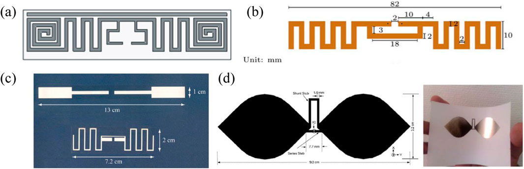
Figure 2. (a–d) Examples of typical printed passive UHF RFID antenna tags. These antennas generally consist of a matching loop and radiating dipole arms. Techniques such as meandering or size reduction are employed to tailor the antenna for specific application requirements. Panel (a,b) is reprinted with permission from ref. (Marindra et al., 2017), Cambridge University Press, 2018, Cambridge University Press. Panel c is reprinted with permission from ref. (Amin et al., 2009), 2009, Institute of Electrical and Electronics Engineers Inc. Panel d is reprinted with permission from ref. (Lee et al., 2011), 2009, Electromagnetics Academy.
Despite these advancements, the high material cost of silver ink limits its economic competitiveness against aluminum-etched alternatives. Manufacturing savings frequently fail to offset precious metal expenses, restricting silver-based printed RFID to high-value applications rather than complete replacement of conventional tags.
2.3 Copper based ink
Copper has emerged as a viable low-cost alternative to silver for RFID antenna fabrication, offering the second-highest intrinsic conductivity (5.96 × 10⁷ S/m) (Wuenscher et al., 2014) among metallic elements, with resource abundance exceeding silver by three orders of magnitude and material costs reduced by 90% (Magdassi et al., 2010; Lee et al., 2009; Li W. et al., 2020). However, copper ink systems must overcome two critical challenges: (i) elevated sintering temperature requirements compared to silver, and (ii) propensity for oxide layer formation (CuO/Cu2O) under ambient conditions. These oxide layers inhibit atomic diffusion during sintering and induce progressive conductivity degradation, leading to printed patterns with compromised initial conductivity and accelerated performance decay (Magdassi et al., 2010; Jeong et al., 2008).
Recent technological developments have introduced multi-pronged strategies to address these challenges. Surface stabilization techniques involving organic protective shells effectively delay copper particle oxidation and at same time prevent aggregation (Grouchko et al., 2009; Zhang et al., 2014b; Yan et al., 2011). However, conventional stabilizers requiring decomposition temperatures (∼300 °C) remain incompatible with temperature-sensitive RFID substrates such as polyethylene terephthalate (PET) and paper. Novel low-temperature stabilizers including 1-amino-2-propanol enable copper pattern formation with 3 × 10⁶ S/m conductivity at 180 °C sintering, but their antioxidative efficacy requires further enhancement (Hokita et al., 2015).
Alternative approaches utilize copper complexes as particle-free precursors, facilitating metallic copper formation at reduced thermal budgets through controlled decomposition pathways, but the method usually suffering from low metal loading (Yabuki et al., 2011; Yang et al., 2023b; Mohan et al., 2025; Xu et al., 2017). Hybrid sintering protocols combining formic acid atmospheres (Hermerschmidt et al., 2018; Li et al., 2018a) with reducing agent additives demonstrate synergistic suppression of oxide formation, while pressure-assisted densification (Komoda et al., 2012; Zeng et al., 2022) and secondary copper layering (Hong et al., 2019) techniques enhance long-term stability by minimizing oxygen/water permeation through microstructural optimization (Tam et al., 2016; Li et al., 2018b).
Notable implementations validate copper’s potential in RFID applications. Kim et al. (Kim et al., 2012) demonstrated that antenna printed from copper complexes exhibit superior surface smoothness (0.23 μm vs. 1.4 μm for silver), reducing AC resistance and enhancing inductance characteristics to achieve wider operational bandwidth (Figure 3c). Hong et al. (Hong et al., 2022) developed screen-printed copper tags attaining 2.1 × 10⁶ S/m conductivity with 170 °C sintering, demonstrating bending durability and 12.8 m read ranges comparable to silver-based systems (Figure 3b). Wang et al. (Wang L. et al., 2023) further reported formic acid-treated copper nanoparticles maintaining 2.2 × 10⁶ S/m conductivity with year-long stability at −4 °C, producing HF/UHF tags with Q-factors exceeding silver counterparts.
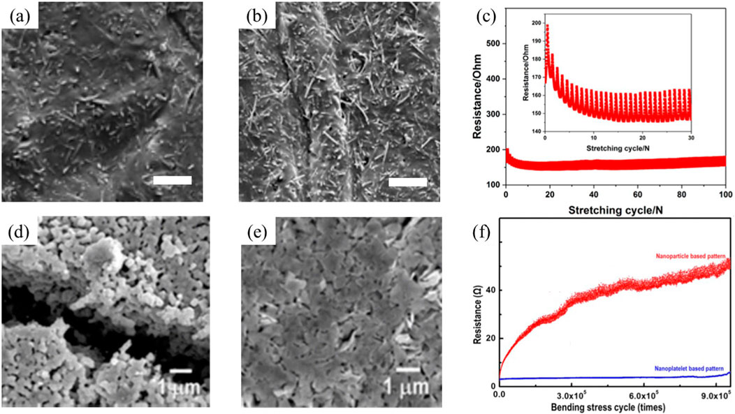
Figure 3. Morphological and electrical characterization of printed conductive patterns. (a–c) Silver nanowire (AgNW)-based patterns: (a,b) SEM image of printed structure before and after stretching, (c) and corresponding resistance-strain response during stretching. (d–f) Ag particle structure evaluation: SEM images of (d) silver nanoparticle (AgNP) and (e) silver nanoplatelet patterns after multicycle stress testing, with (f) their normalized resistance-cycling performance. Panel (a–c) is reprinted with permission from ref. (Huang et al., 2018), 2018, American Chemical Society. Panel (d–f) is Reprinted with permission from ref. (Lee et al., 2013), 2013, American Chemical Society.
Despite these advances, technical and economic barriers persist. Many copper treatment protocols demand specialized equipment or controlled atmospheres that diminish its cost competitiveness. While copper inks show promise for specific applications, current limitations in scalability and process compatibility stopped broad replacement of either silver inks or conventional etching methods.
2.4 Nickel based ink
Nickel is another alternative conductive filler to silver and copper in printed electronics. While nickel demonstrates better oxidation resistance than copper but worse than silver, its electrical conductivity (1.4 × 10⁷ S/m) remains substantially lower than both metals. The material’s high melting point further elevated the necessary sintering temperatures, typically resulting in reduced conductivity compared to silver/copper-based systems (Xie et al., 2023; Park and Kim, 2014). Although nickel inks have shown promise in flexible electronics and sensor applications (Xie et al., 2023; Park and Kim, 2014; Xie et al., 2022), their adoption in RFID antenna manufacturing remains limited. This limitation stems from conflicting requirements in RFID applications: antennas demand both low-temperature processing for substrate compatibility and high conductivity for optimal performance - criteria that nickel-based systems struggle to satisfy simultaneously.
2.5 Low dimensional carbon based Ink
Carbon-based conductive inks present unique advantages for sustainable RFID applications, including natural abundance, environmental compatibility, and resistance to electromigration. While conventional carbon materials like carbon black exhibit insufficient conductivity for antenna applications, low-dimensional carbon (LDC) materials such as carbon nanotubes (CNTs) and graphene demonstrate enhanced potential through their ultrahigh specific surface area and exceptional charge carrier mobility. These properties enable efficient conductive network formation compared with traditional carbon fillers.
Graphene’s two-dimensional honeycomb lattice structure facilitates exceptional in-plane electron mobility (up to 106 cm2/Vs), enabling conductivity approaching metallic levels (Ji et al., 2012; Thodkar and Gramm, 2023; Banszerus et al., 2015). However, achieving this performance requires high-quality single-layer graphene with minimal defects (Tian et al., 2017; Liu et al., 2015; Wei et al., 2011). Production methods like chemical vapor deposition (CVD) (Li et al., 2009; Kim et al., 2009) and silicon carbide epitaxy (Kim et al., 2009; Cao et al., 2018; Song et al., 2025; Merk et al., 2025) can create pristine graphene sheets, but their high costs and low throughput limit practical applications. Liquid-phase exfoliation (LPE) has emerged as the predominant industrial method, where mechanical forces (ultrasonication (Yi and Shen, 2015; Coleman et al., 2011) or shear mixing (Zhao et al., 2010; Paton et al., 2014; Murugadoss et al., 2025)) separate graphite into few-layer graphene flakes within solvents (Torrisi et al., 2012; Parvez et al., 2014; Kadziela et al., 2025; Guo et al., 2025). This process balances quality and scalability, though the resulting flakes typically contain 3–10 atomic layers.
Solvent selection critically influences LPE efficiency. Polar aprotic solvents like N-methyl-2-pyrrolidone (NMP) and dimethylformamide (DMF) effectively exfoliate graphene due to matched surface energy parameters (Shih et al., 2010; Michel et al., 2017; Htwe et al., 2021; Dimitrieva et al., 2024), preventing re-stacking through π-π interactions (Hernandez et al., 2008). However, these solvents pose significant toxicity concerns, driving research into eco-friendly alternatives. Recent advances employ Cyrene™, a biodegradable solvent derived from renewable resources, which achieves comparable exfoliation efficiency without hazardous byproducts (Pan et al., 2018; Salavagione et al., 2017; Tkachev et al., 2021). Water-based exfoliation remains challenging due to graphene’s hydrophobicity, typically requiring surfactants to help dispersion, which degrade conductivity through residual contamination (Dimitrieva et al., 2024).
Pretreatment strategies enhance graphene production efficiency. Expandable graphite precursors, prepared through chemical or electrochemical intercalation, enable rapid exfoliation under microwave irradiation. This pre-expansion weakens interlayer bonds, reducing energy input during subsequent mechanical exfoliation. Post-processing techniques like roll compression further improve conductivity by enhancing flake alignment and interlayer contact (Saidaminov et al., 2012; Lin et al., 2017). Comparing with metallic counterpart, graphene based pattern normally exhibit better resistivity toward bending, but normally need thick layer to achieve RFID demand (Figure 4a) (He et al., 2019).
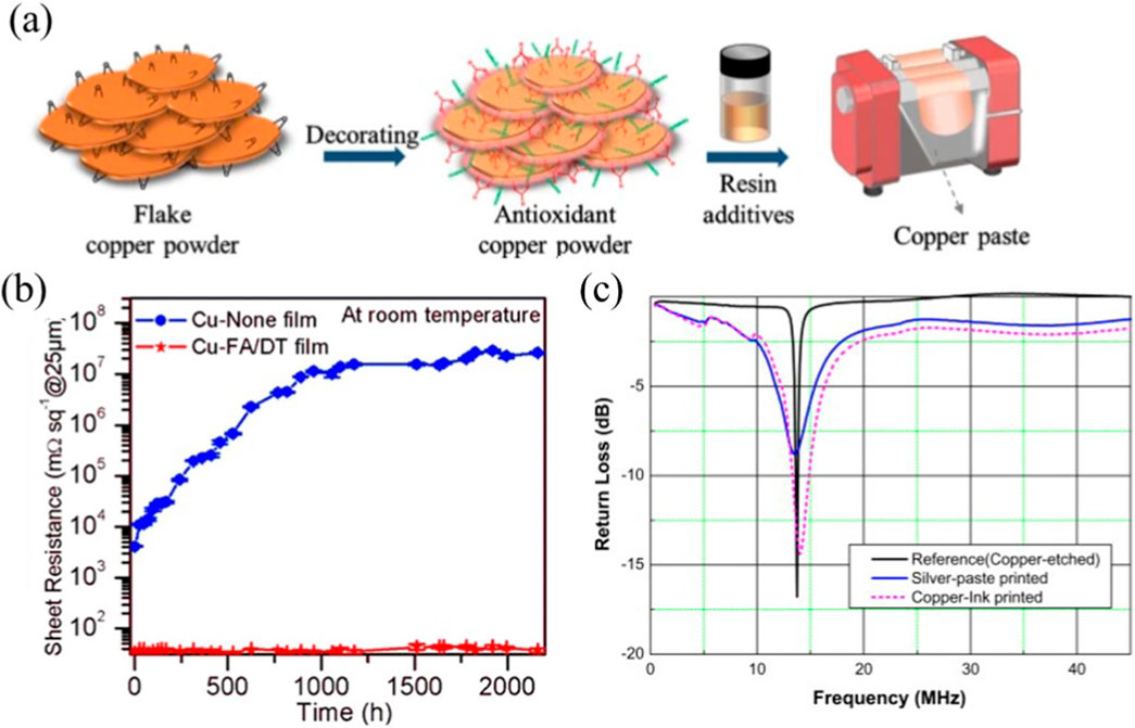
Figure 4. Antioxidant engineering for copper-based conductive inks. (a) Schematic of antioxidant fabrication strategy. (b) Stability comparison between antioxidant-treated (Cu-FA/DT film) and untreated (Cu-None film) copper patterns. (c) Radar plot comparing radio-frequency performance metrics: return loss of etched copper tags, silver printed tags, and copper printed tags. Panel a, b is reprinted with permission from ref. (Hong et al., 2022), 2022, Springer Nature. Panel c is reprinted with permission from ref. (Kim et al., 2012), 2012, Elsevier.
Practical implementations demonstrate the potential of graphene-based RFID tag. Huang et al. (Huang et al., 2015a; Huang et al., 2015b) developed roll-compressed graphene antennas achieving 4.3 × 10⁴ S/m conductivity and 10-m read ranges without binder additives (Figure 4c). Pan et al. (Pan et al., 2018) optimized Cyrene-based LPE parameters to produce antennas with 7.1 × 10⁴ S/m conductivity and 9-m operational range (Figure 4c). Zhou et al. (Zhou et al., 2024) introduced shear-mixed graphene inks offering improved scalability (3 × 10⁴ S/m) with integrated temperature sensing capabilities (Figure 4b). Peng et al. (Xu et al., 2023) employed ball milling to shear graphite into graphene flakes, achieving enhanced conductivity of 1.3 × 10⁵ S/m and RFID tags with 8.9-m operational ranges. Chemically derived reduced graphene oxide (rGO) provides alternative solutions. Sector et al. (Secor et al., 2013) reported rGO inks with conductivities exceeding 2.5 × 10⁴ S/m, while Ozek et al. (Ozek et al., 2021) demonstrated flexible rGO tags capable of 0°–90° bending deformation with high thermal sensitivity (0.0125 °C−1). However, rGO’s higher defect density from oxygen functional groups limits conductivity compared to LPE graphene.
Carbon nanotubes (CNTs) complement graphene in LDC applications, offering unique advantages through their one-dimensional tubular structure (Grado-Caffaro and Grado-Caffaro, 2004; Grado-Caffaro and Grado-Caffaro, 2008). Single-walled CNTs (SWCNTs) exhibit exceptional axial conductivity from defect-free sp2 hybridization, while multi-walled variants (MWCNTs) provide enhanced mechanical stability. Synthesis methods like arc discharge produce high-quality CNTs but remain cost-prohibitive (Zhang et al., 2006; Prasek et al., 2011), whereas chemical vapor deposition (CVD) offers better scalability (Fan et al., 1999; Li et al., 1996). CNT-based inks have demonstrated functionality in gas-sensing RFID tags, especially toward NOx and NH3 (Kong et al., 2000). Li et al. (Yang et al., 2009) developing SWCNT antennas for ammonia detection and Ayesha et al. (Habib et al., 2023) creating MWCNT tags for dual CO2/temperature monitoring.
Although progress, LDC materials face fundamental conductivity limitations compared to metals. Current LDC-based antennas require larger dimensions to compensate for lower conductivity, limiting miniaturization potential. Bridging this performance gap through material engineering and processing optimization remains critical for realizing sustainable carbon-based RFID systems.
2.6 MXene based Ink
MXenes, a class of two-dimensional transition metal carbides/nitrides with the general formula Mn+1XnTx (where M is transition metals, X is carbon/nitrogen, and Tx is surface functional groups), have emerged as promising conductive materials for printed electronics. Their layered structure resembles graphene’s architecture but offers distinct advantages. The partially filled d-orbitals of transition metals in MXenes enable higher charge carrier densities compared to graphene, resulting in superior electrical conductivity even with structural defects. This unique property makes MXenes particularly attractive for printed conductive networks (Lim et al., 2022).
MXene synthesis typically begins with MAX phase precursors (Mn+1AXn, where A is aluminum or silicon group elements). The conventional production method involves selectively etching the A-layer using hydrofluoric acid (HF), which breaks M-A bonds and introduces surface functional groups from the etching solution (Lim et al., 2022; Feng et al., 2017) (Figure 5a). Due to HF’s environmental hazards, alternative etching strategies have emerged including LiF/HCl mixtures (Guo et al., 2020), molten salt systems (Liu et al., 2013), and strong alkaline solutions like NaOH (Ghidiu et al., 2014). Post-etching processes often require intercalation and ultrasonication to separate MXene layers, though excessive additives can increase interflake resistance and reduce conductivity (Xue et al., 2020). While chemical vapor deposition (CVD) provides alternative synthesis routes (Wang D. et al., 2023), its high cost and low throughput same as CVD graphene’s production challenges, limiting the practical applications in conductive inks.
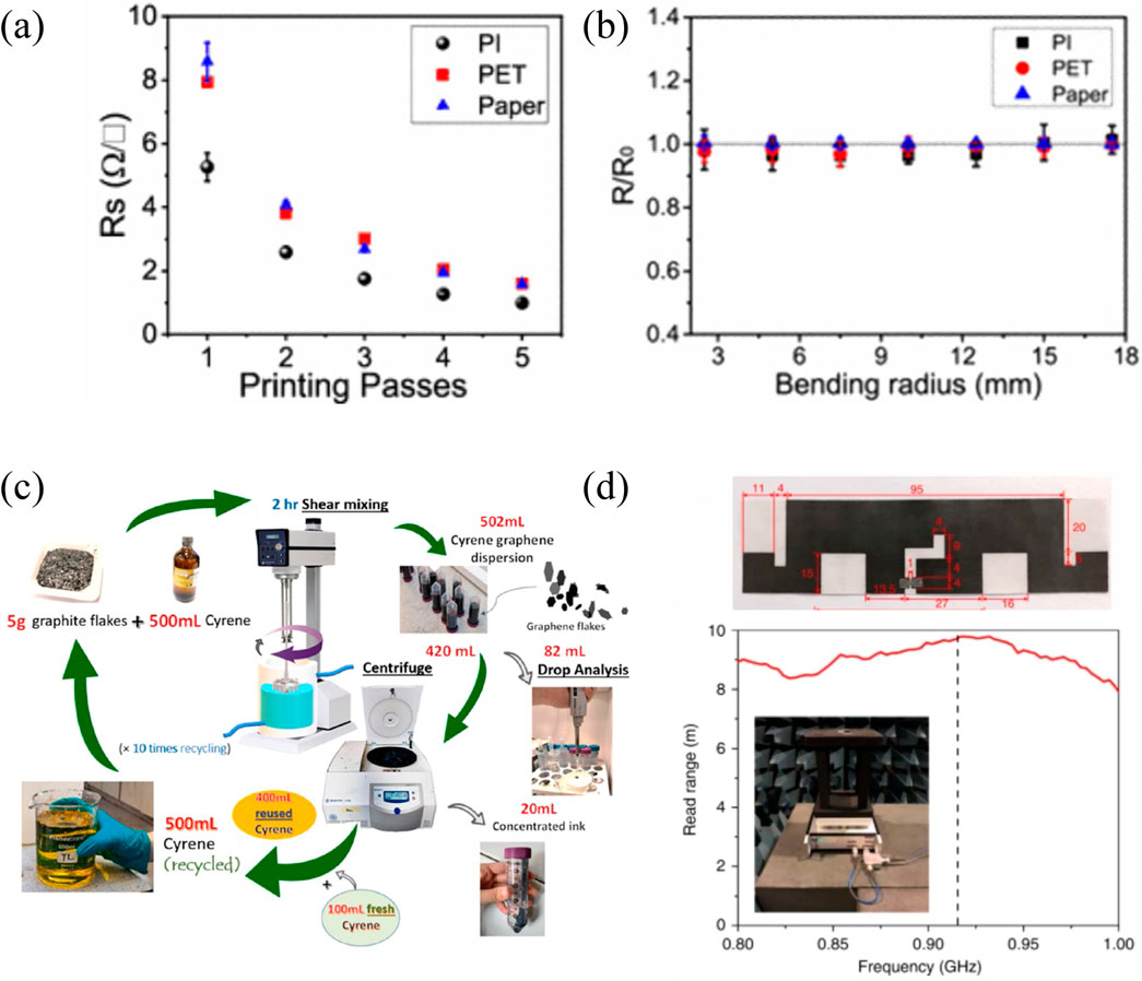
Figure 5. Sustainable graphene engineering and RFID fabrication. (a) Example of graphene printed pattern, sheet resistance vs. printing pass and bending radius, (b) Green graphene production methodology, and (c) an example graphene-based RFID tag with performance evaluation. Panel a is reprinted with permission from ref. (He et al., 2019), 2019, American Chemical Society. Panel b is reprinted with permission from ref. (Zhou et al., 2024), 2023, Elsevier. Panel c is reprinted with permission from ref. (Pan et al., 2018), 2018, Springer Nature.
Recent advancements highlight MXenes’ potential in printed RFID systems (Das et al., 2024; Zhang et al., 2019). Shao et al. (Shao et al., 2022) demonstrated extrusion-printed RFID antennas using Ti3C2Tx MXenes, achieving remarkable conductivity of 7 × 10⁶ S/m - comparable to metallic inks (Figure 5b). The antenna maintains functionality through 500 bending cycles, exhibiting exceptional mechanical durability. Chen et al. (Chen S. et al., 2023) addressed scalability challenges through screen-printed MXene inks with viscosity tuning via sub-micrometer flake optimization, achieving 1.7 × 10⁵ S/m conductivity and RFID tags with 8-m read ranges that retained over 90% performance after 1,000 bending cycles (Figure 5c).
Despite these successes, three critical challenges have to be solved before MXene’s large scale application in RFID industries. Firstly, etching serves as a prerequisite step in the preparation of MXene; however, this process readily introduces uncontrollable surface functional groups (e.g., -F, -OH), which can significantly alter the electronic structure of MXene and, in most cases, remarkably degrade its electrical conductivity. Secondly, the electrical conductivity of MXene is highly dependent on flake characteristics—such as size, thickness, and defect density—parameters that are influenced by both the quality of the precursor MAX phase and the conditions used during exfoliation. Consequently, scaling up MXene ink production from laboratory to industrial levels needs a reliable supply of high-quality MAX phase and precise processing equipment, which may substantially increase manufacturing costs. Finally, as a two-dimensional material, MXene exhibits incomplete coordination of its transition metal atoms, which makes them highly active to oxidation upon exposure to water or oxygen, leading to the formation of metal oxides (e.g., TiO2, V2O5). This oxidation not only disrupts the electronic structure of MXene but also induces structural defects and cracks, resulting in severe deterioration of electrical conductivity. Current research focuses on mild MAX phase etching (Guo et al., 2020), encapsulation techniques and redox-stable MXene formulations (Naguib et al., 2012), but significant technical barriers remain unresolved.
2.7 Multi-filler ink
The pursuit of optimal cost-performance balance in printed electronics has driven development of multi-component conductive inks that combine complementary materials. A prominent strategy involves copper-silver core-shell structures, where a thin silver layer coatings protect low-cost copper cores from oxidation. Grouchko et al. (Grouchko et al., 2009) achieved conductivity comparable to pure silver inks using 40 nm copper nanoparticles with 2 nm silver shells via redox deposition. Pajor-Świerzy et al. (Pajor-Swierzy et al., 2017) demonstrated long-term stability over 6 months using 1 μm copper particles with 40 nm silver layers, maintaining 8 × 10⁶ S/m conductivity. Copper-nickel core-shell systems also show particular promise under extreme conditions (Kim T. G. et al., 2018), like Li et al. (Li et al., 2022a) reporting functional integrity after 180-h exposure to 180 °C and 1,000 bending cycles.
However, synthesizing ideal core-shell structures remains technically challenging. While continuous protective shells theoretically maximize oxidation resistance, practical synthesis through metal displacement reactions often produces discontinuous coatings due to heterogeneous nucleation. Multi-step precipitation methods can improve shell uniformity but introduce procedural complexity that hinders industrial scalability (Njagi et al., 2017). This highlights the need for simplified coating techniques that maintain structural precision while enabling mass production.
Hybrid formulations extend beyond core-shell architectures through strategic material combinations. Incorporating nanocarbon materials to metallic ink enhances both mechanical and electrical performance. For example, adding <1 wt% MWCNTs to copper inks improves electrode uniformity through heterogeneous nucleation while enhancing mechanical durability (Seong et al., 2018). Single-walled carbon nanotubes SWCNTs at 0.5 wt% mixed with Cu ink reduce sintering energy requirements by 30% through improved thermal transfer efficiency (Rosen et al., 2017). Metal blending systems like Cu/Ag and Cu/Ni balance cost and provide partial oxidation resistance (Bhuiyan et al., 2019; Kawamura et al., 2015; Chung et al., 2016), while Li et al. (Li Y. et al., 2020) achieved unprecedented stretchability (∼1,000% strain) and conductivity >106 S/m by integrating self-healing liquid metal into copper ink (Li Y. et al., 2020).
Graphene-silver hybrids demonstrate cost-saving potential without significant conductivity loss. Karim et al. (Karim et al., 2019) replaced 35%–50% silver with graphene while maintaining 1.5 × 10⁶ S/m conductivity through optimized percolation networks. Li et al. (Li et al., 2022b) further enhanced network quality using cysteamine bridging molecules between graphene and silver nanoparticles, achieving over 50% conductivity improvement.
The multi-component systems inherently involve performance trade-offs. Silver-copper hybrids delay oxidation but increase costs compared to pure copper. High nanocarbon loadings improve mechanical properties at the expense of ink jetting consistency. Poor interfacial bonding between dissimilar materials like metals and carbons can degrade electrical pathways.
While multi-component ink facing challenge on different physical behavior and bad wettability between materials, multi-filler ink composed of same component with different morphology have reported with potential to enhance ink performance without the above issue. By strategically combining silver nanoparticles with silver nanowires, researchers achieved significant conductivity enhancement compared to single-morphology systems, attributed to the nanowires’ bridging effect that establishes continuous conductive networks (Shen and Yao, 2016). Similarly, hybrid systems incorporating micron-scale copper particles with copper nanoparticles exhibit improvements in packing density, significantly reducing interfacial resistance through geometric complementarity (Joo et al., 2014). In carbon-based formulations, the addition of carbon black to graphene ink enhances both conductivity and printability through optimized viscoelastic behavior (Liu et al., 2021). While with these advancements, multi-morphology strategies confront inherent material limitations that constrain widespread adoption. Precious metal components maintain prohibitively high costs for silver, while copper-based systems remain vulnerable to oxidation under ambient conditions. Carbon additives exhibit intrinsic conductivity limitations compared to metallic counterparts. More critically, batch-to-batch variations in different filler distribution and morphology consistency also pose significant challenges for industrial-scale manufacturing, requiring precision control which challenges current technological capabilities.
3 RFID antenna design and performance
3.1 Fundamental principles and system architecture
A conventional RFID tag comprises two core elements: an antenna and an integrated circuit (IC). The antenna executes dual operational roles — harvesting electromagnetic energy from the reader’s field to power the IC, and enabling bidirectional data transmission via backscattering modulation (Glidden et al., 2004). When activated, the reader’s interrogation antenna generates RF signals that induce oscillating currents in the tag antenna. These currents power the IC, which modulates the antenna’s impedance characteristics to encode stored data, including unique identification codes, into the reflected signal l (Ghovanloo and Najafi, 2004). Commercial ICs from manufacturers such as Alien Technology and Impinj exhibit inherent capacitive properties, necessitating precise impedance matching with the antenna for optimal frequency alignment.
RFID systems are classified into three operational categories based on power configurations. Active tags with integrated batteries achieve detection ranges exceeding 100 m, albeit with elevated costs and system complexity. Passive tags operate exclusively through harvested RF energy, typically achieving read distances below 12 m. Semi-passive variants combine battery-powered sensors with passive communication modules, balancing energy efficiency and functionality (Glidden et al., 2004). The backscattering mechanism remains central to passive RFID operation, where the tag reflects modulated portions of incident RF energy using amplitude shift keying (ASK) for data encoding (Nikitin and Rao, 2007).
Regional regulatory frameworks impose critical constraints through effective isotropic radiated power (EIRP) limitations. For example, the Federal Communications Commission (FCC) permits 36 dBm (4 W) transmissions in the 902–928 MHz band for North American markets, while the European Telecommunications Standards Institute (ETSI) restricts operations to 33 dBm (2 W) within 865–868 MHz. These regional disparities demand customized antenna optimizations, particularly for commercial off-the-shelf (COTS) components with narrow-band frequency responses (Roy, 2008).
Antenna design optimization requires systematic evaluation of five interdependent parameters. First, IC selection focuses on chips with low activation thresholds (−18 to −22 dBm) to reduce energy demands. Second, achieving conjugate impedance matching between antenna and IC at target frequencies (e.g., 915 MHz) ensures maximal power transfer efficiency. Third, material conductivity directly determines radiation efficiency — traditional etched metal foils (∼107 S/m) outperform printed conductive inks (105–107 S/m), creating cost-performance tradeoffs. Fourth, radiation patterns are application-specific: omnidirectional dipole antennas dominate item-level tracking, while directional patch antennas excel in portal monitoring. Fifth, substrate compatibility requires mechanical adaptations — flexible dipole designs (per commercial UHF standards) incorporate stress-relief patterns for curved surfaces, while metallic substrates necessitate electromagnetic isolation techniques such as λ/4 ground plane spacing.
3.2 Impedance matching
Achieving reliable long-range RFID communication demands precise impedance alignment between the antenna and integrated circuit (IC). Commercial ICs exhibit inherent capacitive properties that must resonate with antenna inductance at operational frequencies (860–960 MHz for UHF systems) to enable efficient energy transfer. The maximum read distance (r) follows Equation 1 (Mehrjerdi, 2011):
where λ corresponds to the operational wavelength, and EIRP (Effective Isotropic Radiated Power) represents region-specific transmitted power limits combining reader antenna gain and output power. The tag antenna’s gain (Gtag) and power transmission coefficient (τ) characterize impedance alignment efficiency. The threshold power (Pth), typically ranging from −18 dBm to −22 dBm for commercial ICs, specifies the minimum energy required for chip activation.
The power transmission coefficient (τ) is defined as in Equation 2:
where Γ denotes the reflection coefficient at the antenna-IC interface, Zc and Za represent chip impedance and antenna input impedance, respectively. Rc and Ra are the real parts of the chip and antenna impedance.
The complex impedances Zc = Rc − jXc (IC) and Za = Ra + jXa (antenna) must adhere to the conjugate matching condition (Ra = Rc, Xa = −Xc) to minimize signal reflection, where Xa and Xc are the imaginary parts of the chip and antenna impedance. Practical implementations frequently employ external matching networks such as T-match or inductive feed structures to compensate for IC parasitic capacitance and antenna reactance (Rao et al., 2005).
Printed RFID systems face two primary challenges in impedance alignment. First, the conductivity of printed conductive inks (105–107 S/m) remains inferior to bulk metals (∼108 S/m), elevating ohmic losses and diminishing antenna gain (Gtag). Second, conductance variations during ink deposition — caused by material packing density, thickness fluctuations, particle orientation, and network defects — induce impedance inconsistencies compromise production consistency in large-scale manufacturing (Kim and Soo, 2013).
3.3 Antenna structure design
RFID antennas integrate impedance-matching elements such as inductive loops with radiating components like dipoles to optimize both power transfer efficiency and radiation characteristics (Figure 6) (Marindra et al., 2017; Amin et al., 2009; Lee et al., 2011). The inverse correlation between antenna quality factor (Q) and operational bandwidth presents a critical design trade-off: high-Q configurations achieve narrow bandwidths suitable for stable operational environments, while low-Q designs enable broadband operation adaptable to dynamic application scenarios (Tsai et al., 2013). This fundamental relationship demands meticulous parameter selection based on deployment-specific electromagnetic conditions and spectral requirements. The input impedance (Zin) at the antenna port is given by Equation 3 and Equation 4:
where Zloop = j2πfLloop represents the loop impedance, M denotes mutual inductance, and Za corresponds to the radiating element’s impedance (Tsai et al., 2013). Commercial ICs exhibit low input impedance (typically 10–50 Ω) with significant capacitive reactance (Xc), need conjugate matching (Za = Zc) to maximize the power transmission coefficient as mentioned in previous section.
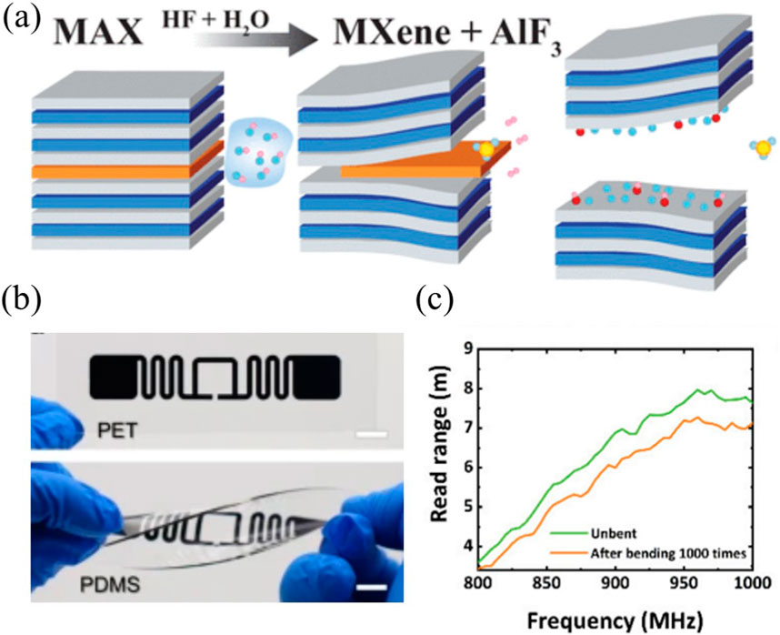
Figure 6. MXene processing and flexible device integration. (a) Illustration of chemical delamination process from MAX phase precursors. (b) Fabricated MXene-based RFID tags on different substrate. (c) Mechanical reliability evaluation showing operational range comparison of printed tags pre-/post-1000 bending cycles. Panel a is reprinted with permission from ref. (Srivastava et al., 2016), 2016, American Chemical Society. Panel b is reprinted with permission from ref. (Shao et al., 2022), 2022, Springer Nature. Panel c is reprinted with permission from ref. (Chen S. et al., 2023), 2023, Springer Nature.
Practical implementations must address parasitic capacitance effects arising from IC placement on antenna terminals. Two primary compensation strategies are widely adopted: T-match networks introduce adjustable LC components to offset parasitic capacitance, achieving impedance alignment, or meandered dipole geometries employ spatial folding techniques to enhance inductive reactance, effectively compensating for capacitive impedance mismatches while maintaining compact antenna dimensions (Tsai et al., 2013).
3.4 Radiation efficiency and conductivity
Radiation efficiency (η) has emerged as a defining performance parameter in RFID antenna design, systematically characterizing the power conversion ratio between radiated power (Prad) and total input power (Prad + Pohmic) (Ostadrahimi et al., 2012), as shown in Equation 5:
Here, Pohmic represents resistive losses in the conductive traces. Impedance mismatches (Za ≠ Zc) and material conductivity limitations jointly degrade η by increasing Pohmic.
For printed antenna architectures, this efficiency metric can be deconvoluted into two distinct factors, impedance mismatching loss (ηmismatch) and conductor resistive loss (ηohm), via Equation 6:
The latter is principally determined by printed pattern conductivity (σ) through the relationship in Equation 7:
where t is the printed conductive layer thickness (typically 5–50 μm for printed antennas). Although increased thickness reduces resistive losses by expanding charge carrier pathways, it simultaneously escalates material consumption. This fundamental constraint presents a critical trade-off between electrical performance and manufacturing cost in printed antenna development.
3.5 Surface morphology and thickness optimization
The radiation efficiency (η) of printed RFID antennas is primarily determined by conductor thickness and surface morphology. Experimental studies confirm that ink thickness below 15 μm significantly increases sheet resistance, thereby degrading signal propagation, while thickness exceeding 50 μm yields diminishing conductivity improvements (Kopyt et al., 2016). Optimal thickness ranges balance material cost and ohmic loss minimization. Surface roughness, which is determined by ink quality and fabrication technique, further compromises performance, particularly in high-current-density regions where morphological irregularities induce localized impedance discontinuities (Shahpari and Thiel, 2015).
The relationship between material roughness,
Here,
where f denotes operating frequency. For typical UHF RFID applications (860–960 MHz), printed antenna require minimum thicknesses >3δ to ensure bulk conductivity (Merilampi et al., 2010). Printing technique selection profoundly determines morphology and thickness control of printed antenna, which will be discussed in next section.
3.6 Substrate selection for printed RFID antennas
Substrate materials exhibit significant impacts on the operational performance and application scope of printed RFID systems. Commercial off-the-shelf (COTS) devices predominantly utilize thin-film substrates including paper and polyethylene terephthalate (PET), with thickness typically 50–100 μm. Paper-based variants account for emerging dominant of global RFID production due to their recyclability and cost-effectiveness (Sajal et al., 2017). Surface functionalization through plasma treatment or chemical coating is also sometimes required to optimize ink adhesion and print resolution (Izdebska-Podsiadly, 2021; J. Izdebska, 2019). Textile substrates (cotton/polyester/silk) have emerged as promising candidates for wearable electronics, yet their inherent morphological characteristics – including surface roughness and porosity – impose significant challenges in achieving high printing accuracy (Guo et al., 2022; Guo et al., 2021). Polymer-based materials such as poly imide (PI) and polyvinyl chloride (PVC) demonstrate superior thermal stability, making them ideal for specific applications requiring wide temperature operation range (Ren et al., 2014).
Substrate thickness modulates antenna performance through dual mechanisms: electromagnetic coupling effects between conductive traces and dielectric interfaces and mechanical stress distribution during flexural deformation. While thicker substrates can induce marginal ohmic losses, these remain negligible compared to conductor-related dissipation in most operational scenarios (Amin et al., 2012). Material selection follows application-specific design strategy: flexible PET accommodates curvilinear surfaces in smart packaging, whereas paper substrates align with disposable medical tracking systems requiring biodegradability (Palazzi et al., 2014). Regulatory compliance with FCC (North American) and ETSI (Europe) standards dictates substrate selection through frequency-dependent permittivity and loss tangent requirements. Advanced engineering solutions employ dielectric spacers to minimize metal surface detuning effects, achieving lower frequency shift in metallic environments. Humidity-resistant polymer formulations are prioritized for outdoor deployment, demonstrating good signal integrity retention (Byondi and Chung, 2019).
3.7 Antenna placement considerations in RFID design
Antenna placement critically influences the performance and reliability of RFID tags. Commercial off-the-shelf (COTS) tags are typically optimized for thin substrates, where minimal performance degradation occurs (Rao et al., 2005). However, placement on thick substrates (e.g., paper layers or metallic surfaces) introduces significant losses and disrupts antenna response due to impedance mismatches and conductive losses. These effects are exacerbated when tags are affixed to high-loss materials such as water or metal, often rendering the tag non-responsive (Michel et al., 2018).
Water and metallic objects behind the tag create parasitic coupling, increasing ohmic losses and impedance mismatches at the chip interface (Michel et al., 2018). While wideband frequency tags offer some adaptability, their performance remains highly sensitive to substrate thickness and material properties. COTS tags are generally designed for specific application scenarios rather than universal use, necessitating careful placement optimization. For unique deployment environments (e.g., glass surfaces), antenna detuning becomes inevitable when the tag operates in free space versus on the target substrate. A practical mitigation strategy involves inserting dielectric spacers (e.g., foam or specialized substrates) between the tag and lossy surfaces to reduce parasitic coupling (Byondi and Chung, 2019).
Bending-induced performance degradation presents another critical challenge. Studies demonstrate that bending near the chip (up to 90°) severely disrupts tag functionality, while side bending causes only minor range reduction (Jiang, 2021). This asymmetry arises from the antenna’s inductive loop design, which suppresses parasitic capacitance from the chip. Consequently, the loop-dominated regions exhibit greater bending tolerance compared to chip-adjacent areas. These findings underscore the importance of mechanical-EM co-design for flexible RFID tags, particularly in applications requiring conformal placement on curved surfaces.
3.8 Chipless RFID
Chipless RFID represents a groundbreaking innovation in the evolution of RFID technology. In contrast to conventional RFID systems that rely on discrete substrates or silicon-based chips, chipless RFID tags are applied directly onto product surfaces or packaging without micro-integrated circuits. This approach streamlines the tagging process, reduces material and manufacturing costs, and greatly expands the potential applications, positioning chipless RFID as a highly versatile solution across numerous industries (Behera, 2022).
Chipless RFID tags are typically composed of printed patterns or spatially designed structures that modulate incident electromagnetic waves—functioning much like RF barcodes or tamper-evident labels (Behera, 2022; Ahmadihaji et al., 2023). Unlike optical methods, chipless RFID systems operate by irradiating tags with electromagnetic signals and decoding the resulting response, which is shaped by the tag’s physical design. This non-line-of-sight capability enables faster read rates, greater operational flexibility, and improved performance in challenging environments, Additionally, chipless tags exhibit greater resilience to mechanical deformations such as bending, as their operation does not depend on rigid chip components or impedance matching. Fabrication methods—often based on printing or etching—are straightforward and scalable, supporting high-volume production at low cost (Sharma and Hashmi, 2021; Barbot et al., 2020; Noman et al., 2023).
Nevertheless, the development of practical reading systems remains a significant challenge. Chipless RFID tags commonly operate at high frequencies over wide bandwidths, typically within the 3.1–10.6 GHz range under licensed spectra. To date, no commercial chipless RFID reader is available; most research implementations rely on costly laboratory instruments such as vector network analyzers (VNAs), which are un-suited for real deployment (Mulloni and Donelli, 2020).
Core reading mechanisms often involve frequency-modulated continuous wave (FMCW) radar or stepped-frequency continuous wave (SFCW) signaling. These methods introduce several difficulties, including sensitivity to tag orientation, reading inaccuracy, multi-tag collisions, and susceptibility to environmental interference. Moreover, operation across broad frequency bands raises issues related to signal integrity, noise, and regulatory compliance (Sharma and Hashmi, 2021; Abbasi et al., 2020). These obstacles must be overcome to enable broad commercial adoption.
Detection methodologies also vary considerably across systems, leading to inconsistency in readout performance and reliability. Although chipless RFID remains largely in the research and pilot stage, emerging approaches—particularly machine learning (ML)—offer promising pathways to address these shortcomings. ML algorithms can enhance signal interpretation, adapt to varying tag orientations, mitigate multi-tag interference, and improve robustness under noisy conditions. By integrating adaptive learning into response analysis, ML can standardize detection and accelerate the transition of chipless RFID from laboratory prototypes to practical applications (Zhao et al., 2025).
4 Fabrication techniques
Printing technology fundamentally determined the functional performance and manufacturing scalability of RFID antennas, with critical parameters including conductive network morphology, surface roughness, and film thickness distribution. Recent advancements in additive manufacturing have established explicit correlations between printing process parameters and pattern electromagnetic characteristics (Table 1).
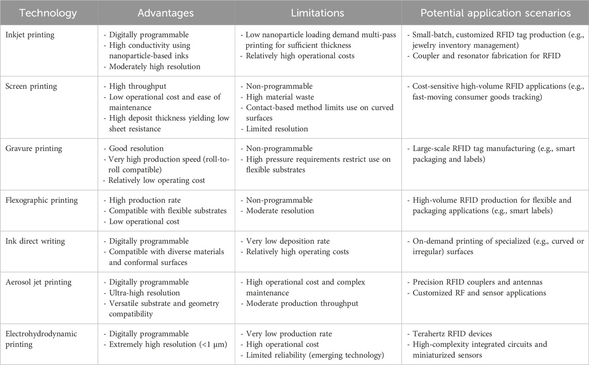
Table 1. Comparative analysis of printed manufacturing technologies for RFID applications.
4.1 Inkjet printing
Inkjet printing has emerged as a predominant non-contact patterning method for RFID antenna fabrication, achieving micrometer-scale resolution through controlled droplet deposition (Figure 7a). Two distinct operational modalities dominate industrial applications: continuous inkjet (CIJ) and drop-on-demand (DOD) systems (Phung and Kwon, 2022). While CIJ employs electrostatic guidance for high-throughput conductive fluid deposition, its material compatibility constraints with functional inks have limited adoption in flexible electronics. DOD method can overcome these limitations. This technique employing thermal, piezoelectric, or acoustic actuation mechanisms to eject droplets on demand, ensuring substrate versatility and fine pattern control (Khalil et al., 2025; Zhao et al., 2021).
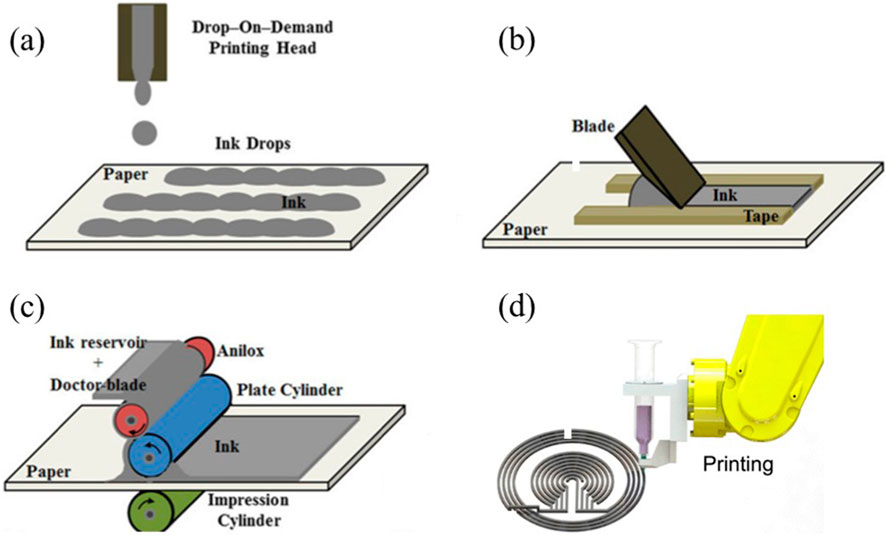
Figure 7. Illustration of inkjet printing (a), screen printing (b), flexographic printing (c) and ink direct writing (d). Panel (a–c) is reprinted with permission from ref. (Srivastava et al., 2016), 2015, Springer Nature. Panel d is reprinted with permission from ref. (Kalhori and Kim, 2022), 2022, American Chemical Society.
The printability of conductive inks depends critically on nozzle geometry (diameter α) and ink properties—particularly viscosity (η, 1–25 mPa s), surface tension (γ, 25–50 mN/m), and density (ρ) (Kiliszkiewicz, 2024). These parameters collectively define the dimensionless Z-number (Jang et al., 2009):
which indicating the droplet formation dynamics, with optimal printability occurring at Z = 4–14 (Jang et al., 2009). While inkjet printing has been widely examined for printed electronics, its implementation in RFID antennas faces material-specific challenges. Silver nanoparticle inks achieve near-copper performance when paired with optimized antenna structure and sintering protocols (Orecchini et al., 2010). In contrast, graphene-based inks typically exhibit insufficient conductivity (<104 S/m) for RFID applications (Huang et al., 2015a), though multicycle printing combined with high-pressure compression has demonstrated viability (>4 × 10⁴ S/m) (Karim et al., 2017). The low viscosity and non-contact droplet addition method of inkjet printing inherently limit conductive filler amount during printing, creating thin film and sparse of interparticle networks after sintering. This bottleneck reduces thickness and need multi-cycle deposition strategies to enhance the cross section area (Hamidon et al., 2024). However, this method significantly reduces production rates while increasing alignment errors and resolution loss (Colella et al., 2017). The trade-off between conductivity enhancement and manufacturing efficiency remains a key challenge for inkjet-printed RFID antennas.
4.2 Screen printing
Screen printing has emerged as a pivotal contact-based manufacturing technique for radio frequency identification (RFID) antenna fabrication, particularly valued for its high-throughput capabilities in industrial-scale production. This mature patterning technology utilizes precision-engineered mesh stencils - typically fabricated from polyamide, polyester, or stainless steel with controlled mesh densities - to transfer functional materials onto flexible substrates (Pan et al., 2018; Chen S. et al., 2023). During the deposition process, viscous conductive pastes are mechanically forced through the emulsion-free apertures via a computer or mechanical-controlled squeegee system, achieving high resolution pattern with tight dimensional tolerance (Parashkov et al., 2005).
Optimal pattern fidelity depends on synchronized parameter adjustments, including ink viscosity, squeegee angle, mesh count, printing speed, and applied pressure (Parashkov et al., 2005). Comparative studies reveal that: screen-printed antennas exhibit lower conductivity than inkjet-printed counterparts due to residual solvents in high-viscosity inks. However, the thicker conductive layers achievable through screen printing reduce radio frequency (RF) losses, enhancing overall antenna efficiency (Salmeron et al., 2014). Materials such as silver (Salmeron et al., 2014), copper (Kim et al., 2012), graphene (Pan et al., 2018), and MXene (Chen S. et al., 2023) have demonstrated viability for screen-printed RFID tags, with performance approaching that of traditional etched copper antennas.
Two persistent technical barriers currently limit this method from broader industrial adoption: surface morphology irregularities induced by mesh-texture transfer effects, and suboptimal material utilization efficiency compared to drop-on-demand inkjet systems (Bjorninen et al., 2009).
4.3 Gravure printing
Gravure printing serves as a widely implemented manufacturing technique in printed electronics, employing laser-etched cylinders to transfer conductive inks onto flexible substrates. During operation, the engraved cylinder rotates through an ink reservoir, where excess ink is removed by a blade, leaving material only within the recessed patterns. When the cylinder contacts the substrate under optimized surface energy conditions, the retained ink transfers to form precise antenna geometries. Three critical parameters determine printing quality: ink viscosity, substrate speed, and impression roller pressure (Abbel et al., 2018).
Despite its inherent advantages in roll-to-roll production throughput, gravure printing faces limited adoption in RF antenna manufacturing due to conductivity constraints. Conventional gravure-printed antennas exhibit significantly lower conductivity compared to etched copper counterparts, primarily due to ink formulation limitations (Nguyen et al., 2017; Allen et al., 2011). Recent developments in multi-pass printing strategies have partially addressed this challenge (Choi et al., 2010; Park et al., 2012; Allen et al., 2011), enabling roll-to-roll fabrication of RFID tags with radiation efficiencies reaching 60% of traditional etched antennas (Choi et al., 2010). Line missing during printing is another essential issue for gravure printing, which directly dropped the quality control during industrial scale production, thus accurate parameter control (like grey-based Taguchi method) is needed, which pose additional barrier for its industrial use (Nguyen et al., 2017).
4.4 Flexographic printing
Flexographic printing serves as a rapid roll-to-roll manufacturing method suitable for antenna fabrication. Unlike gravure printing, this technique employs raised relief patterns on flexible polymer plates to transfer ink, analogous to a stamping mechanism. During operation, a perforated ceramic roller draws ink from the reservoir, with excess ink removed by a doctor blade. The roller’s micro-pores precisely meter the ink volume, transferring it to the raised plate areas during rotation (Figure 7c). These inked patterns are subsequently stamped onto the substrate through controlled pressure. Critical process parameters influencing pattern fidelity include roller gap settings, printing speed, and ink volume control (Shrestha et al., 2019).
Despite progress in printed electronics applications, flexography faces resolution limitations compared to gravure methods, restricting its adoption in high-frequency RF antenna manufacturing. A notable study successfully demonstrated microwave RFID tag production via flexographic printing using silver nanoparticle inks, achieving satisfactory radar cross-section performance (Shrestha et al., 2019). Comparative analyses with screen printing method reveal flexography’s superior production rates but worse quality control during RFID production (Dokic et al., 2015).
4.5 Ink direct writing
Ink Direct Writing (IDW) has emerged as a promising fabrication method for printed RFID antennas. This technique employs pneumatic pressure to extrude conductive ink through a syringe nozzle onto substrates, coupled with a programmable three-axis robotic arm that progressively builds antenna structures through layer-by-layer deposition. Unlike conventional planar printing techniques, IDW demonstrates exceptional substrate compatibility, enabling antenna fabrication on both flat surfaces and complex three-dimensional geometries—a critical advantage for applications involving textiles or curved electronics (Figure 7d).
Recent advancements confirm IDW’s capability to produce functional RFID antennas using silver (He et al., 2017), graphene (Akbari et al., 2017), and MXene-based inks (Shao et al., 2022). These implementations achieve performance metrics comparable to screen-printed and inkjet-printed counterparts while offering superior adaptability to non-planar surfaces. Although IDW typically exhibits lower resolution than other methods, studies demonstrate that optimizing ink parameters—including conductive filler concentration, particle size distribution, and shear-thinning rheology—can enhance printing precision to match inkjet printing standards and exceed screen printing capabilities (Shao et al., 2022).
The primary limitation of IDW lies in its relatively low production efficiency. Typical printing speeds of approximately 1 m/min is significantly below the previous mentioned mainstream methods like inkjet (∼10 m/min), screen (∼50 m/min), gravure (∼100 m/min), and flexographic printing (∼100 m/min) (Kalhori and Kim, 2022). This speed constraint currently restricts IDW’s industrial scalability in near future.
4.6 Emerging printing technologies
Driven by growing demands for precise, programmable, and material-compatible manufacturing, several advanced printing technologies have recently been developed, including Aerosol Jet Printing (AJP) and Electrohydrodynamic Printing (EHDP).
AJP employs an atomization module to generate aerosol droplets (diameter <5 μm) from functional nano-inks through ultrasonication or pneumatic energy. These aerosol droplets are transported by a carrier gas into a print head, where an annular sheath gas stream surrounds and focuses the aerosol flow into a tightly constrained jet. This jet is then ejected from the nozzle and deposited onto the target substrate. Notably, this focusing mechanism allows the printed stream to be significantly finer than the nozzle diameter, enabling high-resolution patterning even with a standoff distance between the print head and the substrate (Secor, 2018). This unique feature effectively merges the benefits of direct ink writing (DIW), such as compatibility with non-planar surfaces, with those of inkjet printing, with high printing precision. AJP has demonstrated considerable potential for fabricating RFID tags, utilizing various conductive inks including silver (Verma et al., 2025), silver–MXene composites (Niu et al., 2025), and graphene (Gamba et al., 2023). It enables the fabrication of antennas with programmable geometries, showing particular promise for chipless RFID and smart packaging applications. Despite these advantages, AJP currently faces challenges in throughput, largely due to the typically low solid content of metallic nanoparticle inks, which often need multiple printing passes (Secor, 2018). Although multi-nozzle configurations combined in-line drying have been shown to improve throughput (Guyll et al., 2024), issues related to system complexity, maintenance, and ink formulation remain significant obstacles to large-scale application.
EHDP represents another emerging high-resolution additive manufacturing technique. This process utilizes a strong electric field applied between the nozzle and the substrate, which polarizes the nozzle tip and induces the formation of a Taylor cone. Once the electric field exceeds a critical threshold, a stable micro-jet is ejected from the cone apex and deposited onto the substrate. Given that the jet originates from a nanometric meniscus, EHDP currently achieves the highest resolution among printing methods, with feature sizes reaching sub-100 nm (Ma et al., 2023). Although EHDP has been successfully applied in flexible electronics (Zhang et al., 2020; Yin et al., 2024), its use in RFID manufacturing remains limited. This is largely because conventional RFID systems operate in the MHz to GHz range (wavelengths from meters to centimeters), where the extreme resolution of EHDP offers negligible benefits, while its drawbacks—such as low printing speed and high operational costs—become more significant. However, as the demand for higher response rates and data transmission capacities grows, EHDP is anticipated to play a critical role in the development of next-generation ultrahigh-frequency RFID systems, such as those operating in the terahertz (THz) regime, where its exceptional precision will be the most important advantage.
5 Summary and perspectives
The development of printed RFID technology has reached a critical transition point from laboratory validation to industrial implementation. As detailed in previous sections, recent advancements in conductive inks, antenna design, and printing methodologies have demonstrated the feasibility of printed RFID tags in specialized applications, showcasing inherent advantages in flexibility and environmentally sustainable manufacturing compared to traditional etching processes (Table 2). However, the widespread industrial application of these technologies continues to face multifaceted challenges that demand systematic solutions.
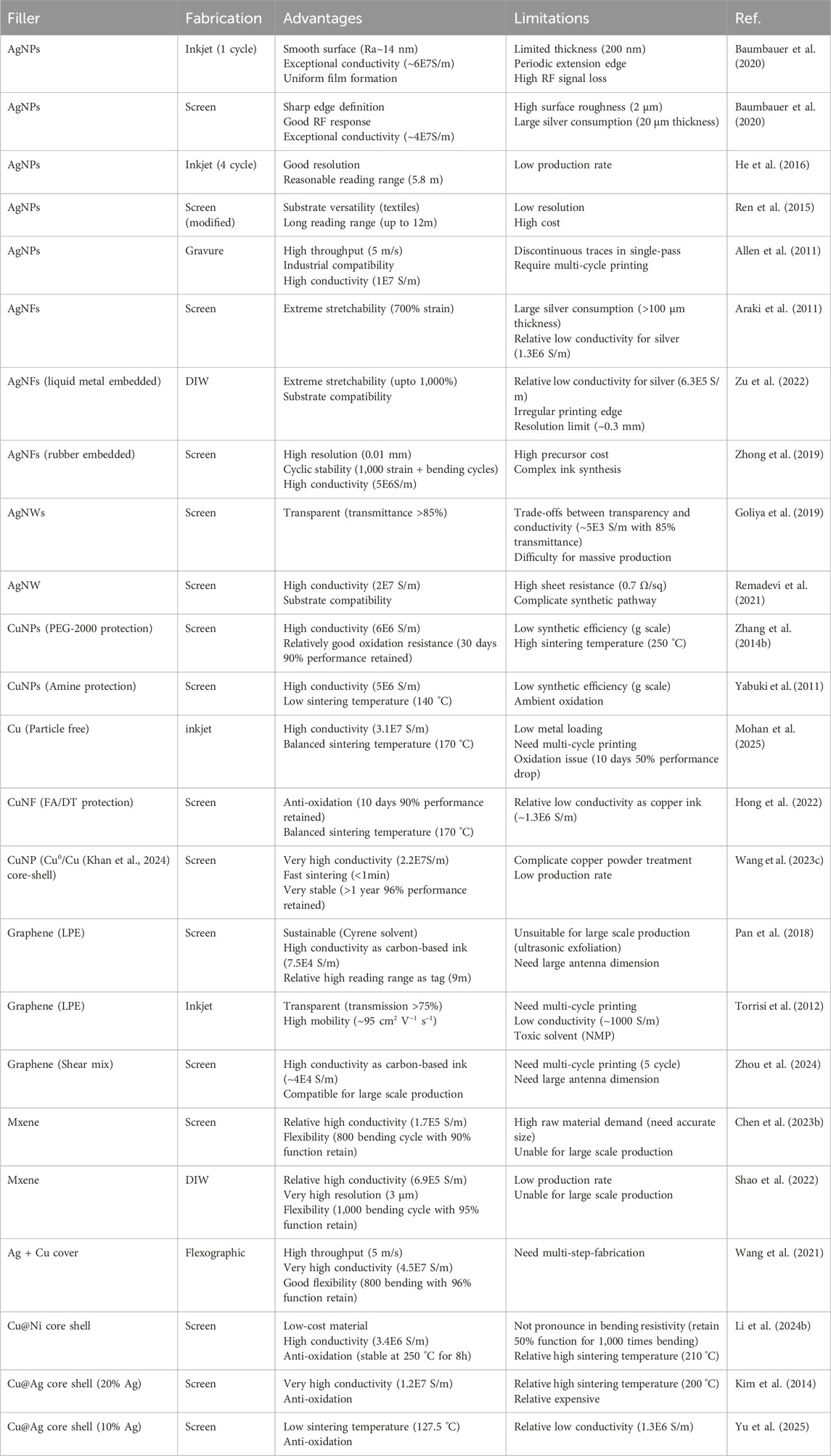
Table 2. Advantage and limitations of reported printed pattern/tag with different fillers and fabrication methods.
The principal constraint in the development of printed radio-frequency identification (RFID) tags stems from the inherent limitations of conductive fillers (Table 3). Although silver-based RFID systems have reached commercial viability, their high manufacturing costs remain a barrier to broad implementation. Scaling up production of printed RFID technology will require abundant and cost-effective materials. Copper-based composites represent the most promising near-term (within 2–3 years) alternative to silver, owing to copper’s excellent intrinsic electrical conductivity, while the issue of its oxidative instability. While recent advances have demonstrated antioxidant copper inks with ambient stability comparable to that of silver (see Section 2.3), these formulations often depend on precise processing conditions. The impact of such treatments on manufacturing cost and production throughput at an industrial scale remains poorly quantified and represents a critical gap in the current literature. Furthermore, ensuring consistent treatment quality during the transition from laboratory to industrial production poses additional challenges. In the long term, low-dimensional carbon (LDC) materials may emerge as an ideal candidate for printed RFID applications, due to the exceptional abundance and environmental stability of carbon. However, despite decades of research and numerous notable advances (see Section 2.4), the electrical conductivity of LDCs remains orders of magnitude lower than that of metals. High-quality LDCs often command a cost exceeding that of noble metals such as silver, without delivering superior performance, whereas lower-quality LDCs exhibit graphitic rather than metallic conduction. Barring a fundamental breakthrough, LDCs are unlikely to serve as the primary material for printed RFID in the foreseeable future. Nonetheless, their unique attributes—including high specific surface area, mechanical flexibility, and environmental sensitivity—make them suitable for specialized applications such as metallic ink additives, RF sensors, and large-area flexible tags. Similarly, MXenes, as two-dimensional materials, face challenges analogous to those of LDCs (particularly graphene). Although the d-orbitals of transition metal atoms provide additional charge carriers—yielding higher intrinsic conductivity than LDCs—these undercoordinated sites also facilitate oxidation. Moreover, unlike graphite (the precursor for graphene), high-quality MXene precursors (MAX phases) remain difficult to synthesize at scale, rendering large-scale production impractical in the short term. Current efforts toward industrialization of printed RFID tags should prioritize the development of multi-material architectures designed to optimize percolation networks. For instance, the large specific surface area of graphene can bridge unpercolated silver nanoparticles, substantially reducing silver usage without significantly compromising electrical performance. Liquid metals, offering self-healing capabilities, show promise in protecting copper (or silver-coated copper) from oxidation while enhancing bending durability. Another significant challenge in printed RFID fabrication lies in the curing process. Flexible and sustainable substrates are often unable to withstand high temperatures, yet lower curing temperatures prove insufficient to activate effective particle percolation, leading to elevated interfacial resistance and compromised electrical performance. Particle-free ink systems with high metal-loading capacity offer a promising solution by reducing curing requirements and enhancing printing resolution, thereby representing a strategic direction for advancing printable electronics. To overcome these limitations, next-generation conductive ink development may focus on two critical pathways. First, improving electronic transport efficiency requires optimizing conductive network architecture through increased specific surface area of fillers while minimizing defect susceptibility. Second, use particle free printing strategy using metal-complex with high metal loading capacities. The formulation of conductive networks and rheological control in inks depend not only on filler properties but also on binder characteristics, carrier fluid parameters, and additive compositions. Advanced computational platforms demonstrate significant potential for efficiently screening material combinations with tailored properties. When combined with AI-driven approaches for material design and performance prediction, these computational tools may accelerate the development of optimized conductive ink systems.
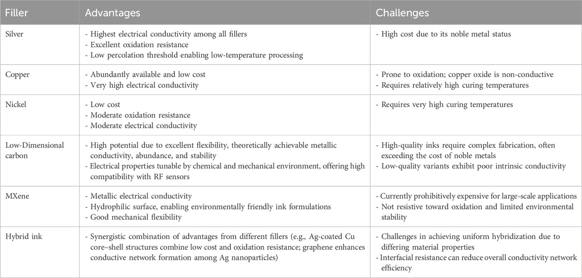
Table 3. Comparative overview of conductive fillers for printable electronics.
Miniaturizing antennas without compromising read-range performance remains a key design challenge, requiring multi-parameter coordination for application-specific structural optimization. Beyond this, reducing ink consumption through antenna design—such as replacing traditional solid structures with grid or hollow dipole structures—is an important approach to balancing cost and performance in printed tags. Furthermore, dual-frequency tag design, metal-interference-resistant RFID solutions, and the application of neural network systems represent major trends in next-generation antenna development.
The inherent trade-off between print quality and production speed remains a persistent challenge in printed RFID tag fabrication. Addressing this limitation requires not only advancements in printing techniques but also coordinated optimization of ink rheology, deposition uniformity, and antenna architecture design, which require a multidisciplinary collaborative approach. Although theoretical models for printing processes have been established, parameter optimization in practical implementations remains predominantly empirical. Deep integration of printing simulations with ink-substrate interaction dynamics and conductive network formation mechanisms will be critical for overcoming current technological barriers. Emerging technologies such as electrohydrodynamic (EHD) printing, which enables precise droplet control at the micrometer scale, demonstrate potential to transcend conventional resolution-speed trade-offs, positioning this methodology as a pivotal focus for future development (Zhang et al., 2020).
With above three aspects, breakthroughs in individual field may yield highly attractive lab-scale prototype tags, the comprehensive integration and coordination of all these factors will be the core challenge in bridging the gap between lab prototypes and industrial-scale production for printed RFID technology. AI technology holds significant potential to address the critical coupling challenges among material selection, structural design, and printing processes. Current research demonstrates that machine learning algorithms can optimize key printing parameters (including speed, flow pressure, and filler concentration) while established predictive models that correlate printing parameters with product performance. This data-driven approach effectively alternate the traditional time-consuming trial-and-error procedures in process development (Thummalapalli et al., 2024; Hashemi et al., 2024; Chitre et al.). For instance, Sri et al. integrated the K-Nearest Neighbors (KNN) algorithm with a VGG16 convolutional neural network (CNN) for image feature extraction to predict and classify print quality in direct ink writing (DIW). By correlating printing parameters—such as speed, pressure, and filler concentration—with print outcomes, their KNN model facilitated automated quality assessment without the need for extensive experimental iterations. Furthermore, the framework demonstrated potential for real-time monitoring and dynamic parameter adjustment, thereby ensuring consistent print quality and optimized material performance (Thummalapalli et al., 2024).
Furthermore, AI also shows promising potential in conductive filler design. The data-driven modeling enables the prediction of structure-property relationships (e.g., between material architecture and electrical conductivity) and performance evaluation of novel materials. The integration of product similarity analysis with reaction optimization could facilitate the development of efficient conductive filler fabrication pathways (Coley et al., 2017). Notably, Sui et al. employed Graph Attention Networks (GAT) in conjunction with hybrid particle-field molecular dynamics (hPF-MD) simulations and resistor network analysis to elucidate the conductive network formation of carbon nanotubes (CNTs) within a homopolymer matrix and to accurately predict electrical conductivity. Their methodology involved extracting simulation snapshots and key structural features to construct a graph-based dataset, which was then used to train a GAT model for conductivity regression. This approach not only uncovered the influence of CNT concentration on network connectivity but also identified an optimal concentration of 7% for maximizing electrical conduction. The study highlights the potential of machine learning to guide the formulation of conductive composites and the rational design of functional network architectures (Sui et al., 2025). Machine learning combined with big data platforms shows particular potential for accelerating innovation in printable RFID industries.
However, two fundamental challenges must be resolved before systematic implementation of AI in printed RFID tag production: 1) Establishment of high-quality, standardized datasets encompassing material characteristics, process parameters, and performance metrics; 2) Development of synthesis/design/prediction systems that strictly adhere to fundamental physicochemical principles, while maintaining both rationale and computational efficiency. Addressing these challenges will determine the practical viability and scalability of AI applications in this field.
Although silver-based conductive ink printed RFID tags have achieved initial commercialization, their widespread adoption remains constrained by limited cost competitiveness relative to conventional etched copper/aluminum-based RFID systems. Nevertheless, in alignment with global sustainability initiatives, the environmentally friendly attributes of printed RFID technology—characterized by reduced material waste and lower pollution throughout the production process—are anticipated to strengthen its market position. Concurrently, ongoing advancements in low-cost functional inks, including silver-coated copper, pure copper, and metal-graphene hybrid formulations, are expected to minimize existing economic barriers. It is projected that within the next 2–3 years, printed RFID tags will progressively supplant traditional etched counterparts in a range of applications. Over the subsequent 4–7 years, accelerated by the expansive growth of the IoT, RFID functionality is anticipated to evolve from mere product identification toward enhanced roles in sensing and monitoring. In this context, printed RFID platforms—featuring intrinsic material sensitivity and flexibility for conformal and wearable integration—are likely to demonstrate distinct advantages in emerging sensing applications. Furthermore, with anticipated development of chipless RFID architectures and artificial intelligence (AI)-driven automated design tools, the realization of programmable and reconfigurable printed RFID systems appears feasible. Those developments are poised to establish printed RFID as a mainstream technology in the flexible electronics and IoT markets.
Author contributions
XW: Funding acquisition, Writing – review and editing, Writing – original draft, Project administration, Conceptualization, Methodology, Supervision. MK: Methodology, Writing – original draft, Supervision, Writing – review and editing. WJ: Writing – original draft, Resources, Writing – review and editing, Investigation. ZT: Methodology, Writing – original draft, Investigation, Writing – review and editing. ZW: Writing – review and editing, Writing – original draft, Investigation. AZ: Writing – review and editing, Writing – original draft, Investigation. NW: Writing – original draft, Writing – review and editing, Investigation. XL: Funding acquisition, Writing – original draft, Investigation, Supervision, Writing – review and editing.
Funding
The author(s) declare that financial support was received for the research and/or publication of this article. X. Wang, N. Wei, W. Jiang and X. Li acknowledge the support from Wenzhou Major Science and Technology Innovation Key Project (No. ZG2024058).
Conflict of interest
The authors declare that the research was conducted in the absence of any commercial or financial relationships that could be construed as a potential conflict of interest.
Generative AI statement
The author(s) declare that no Generative AI was used in the creation of this manuscript.
Any alternative text (alt text) provided alongside figures in this article has been generated by Frontiers with the support of artificial intelligence and reasonable efforts have been made to ensure accuracy, including review by the authors wherever possible. If you identify any issues, please contact us.
Publisher’s note
All claims expressed in this article are solely those of the authors and do not necessarily represent those of their affiliated organizations, or those of the publisher, the editors and the reviewers. Any product that may be evaluated in this article, or claim that may be made by its manufacturer, is not guaranteed or endorsed by the publisher.
References
Abbasi, Z., Baghelani, M., and Daneshmand, M. (2020). High-resolution chipless tag RF sensor. IEEE Trans. Microw. Theory Tech. 68, 4855–4864. doi:10.1109/tmtt.2020.3014653
Abbel, R., Galagan, Y., and Groen, P. (2018). Roll-to-Roll fabrication of solution processed electronics. Adv. Eng. Mater. 20, 1701190. doi:10.1002/adem.201701190
Ahmadihaji, A., Izquierdo, R., and Shih, A. (2023). From chip-based to chipless RFID sensors: a review. IEEE Sensors J. 23, 11356–11373. doi:10.1109/jsen.2023.3266316
Akbari, M., He, H., Juuti, J., Tentzeris, M. M., Virkki, J., and Ukkonen, L. (2017). Int. J. Antennas Propag. 2017, 7327398. doi:10.1155/2017/7327398
Allen, M., Lee, C., Ahn, B., Kololuoma, T., Shin, K., and Ko, S. (2011). R2R gravure and inkjet printed RF resonant tag. Microelectron. Eng. 88, 3293–3299. doi:10.1016/j.mee.2011.08.010
Amendola, S., Lodato, R., Manzari, S., Occhiuzzi, C., and Marrocco, G. (2014). RFID technology for IoT-Based personal healthcare in smart spaces. Ieee Internet Things J. 1, 144–152. doi:10.1109/jiot.2014.2313981
Amin, Y., Prokkola, S., Shao, B., Hallstedt, J., Tenhunen, H., and Zheng, L. R. (2009).Prog. Electromagn. Research-Pier 126, 49–64. doi:10.2528/pier1202085
Amin, Y., Chen, Q., Tenhunen, H., and Zheng, L. R. (2012). Prog. Electromagn. Research-Pier 126, 49–64. doi:10.2528/pier12020805
Araki, T., Nogi, M., Suganuma, K., Kogure, M., and Kirihara, O. (2011). Printable and stretchable conductive wirings comprising silver flakes and elastomers. Ieee Electron Device Lett. 32, 1424–1426. doi:10.1109/led.2011.2161663
Banszerus, L., Schmitz, M., Engels, S., Dauber, J., Oellers, M., Haupt, F., et al. (2015). Ultrahigh-mobility graphene devices from chemical vapor deposition on reusable copper. Sci. Adv. 1, 1500222. doi:10.1126/sciadv.1500222
Barbot, N., Rance, O., and Perret, E. (2020). Angle sensor based on chipless RFID tag. IEEE Antennas Wirel. Propag. Lett. 19, 233–237. doi:10.1109/lawp.2019.2955890
Baumbauer, C. L., Anderson, M. G., Ting, J., Sreekumar, A., Rabaey, J. M., Arias, A. C., et al. (2020). Printed, flexible, compact UHF-RFID sensor tags enabled by hybrid electronics. Sci. Rep-Uk 10, 16543. doi:10.1038/s41598-020-73471-9
Behera, S. K. (2022). Chipless RFID sensors for wearable applications: a review. IEEE Sensors J. 22, 1105–1120. doi:10.1109/jsen.2021.3126487
Bhuiyan, M. E. H., Behroozfar, A., Daryadel, S., Moreno, S., Morsali, S., and Minary-Jolandan, M. (2019). A hybrid process for printing pure and high conductivity Nanocrystalline copper and nickel on flexible polymeric substrates. Sci. Rep-Uk 9, 19032. doi:10.1038/s41598-019-55640-7
Bin Ahmad, M., Lim, J. J., Shameli, K., Ibrahim, N. A., and Tay, M. Y. (2011). Synthesis of silver nanoparticles in Chitosan, Gelatin and Chitosan/Gelatin bionanocomposites by a chemical reducing agent and their characterization. Molecules 16, 7237–7248. doi:10.3390/molecules16097237
Bjorninen, T., Merilampi, S., Ukkonen, L., Sydanheimo, L., and Ruuskanen, P. (2009). Int. J. Antennas Propag. 2009, 920947. doi:10.1155/2009/920947
Byondi, F. K., and Chung, Y. (2019). Longest-Range UHF RFID sensor tag antenna for IoT applied for metal and non-metal objects. Sensors-Basel 19, 5460. doi:10.3390/s19245460
Cao, Y., Fatemi, V., Demir, A., Fang, S., Tomarken, S. L., Luo, J. Y., et al. (2018). Correlated insulator behaviour at half-filling in magic-angle graphene superlattices. Nature 556, 80–84. doi:10.1038/nature26154
Chen, X., Zhang, Y., Ma, C., and Liu, H. (2023a). Large-area, stretchable, ordered silver nanowires electrode by superwetting-induced transfer of ionic liquid@silver nanowires complex. Chem. Eng. J. 476, 146505. doi:10.1016/j.cej.2023.146505
Chen, S., Fu, H., Si, Y., Liu, X., Wang, Z., Duan, Y., et al. (2023b). Size effect enabling additive-free MXene ink with ultrahigh conductivity for screen printing of wireless electronics. Nano Res. 16, 11012–11017. doi:10.1007/s12274-023-5762-3
Chitre, A., Querimit, R. C. M., Rihm, S. D., Karan, D., Zhu, B., Wang, K., et al. (2024). Sci. Data 11, 782. doi:10.1038/s41597-024-03573-w
Choi, B. O., Kim, C. H., and Kim, D. S. (2010). Manufacturing ultra-high-frequency radio frequency identification tag antennas by multilayer printings. Proc. Institution Mech. Eng. Part C-Journal Mech. Eng. Sci. 224, 149–156. doi:10.1243/09544062jmes1610
Chung, W.-H., Hwang, Y.-T., Lee, S.-H., and Kim, H.-S. (2016). Electrical wire explosion process of copper/silver hybrid nano-particle ink and its sintering via flash white light to achieve high electrical conductivity. Nanotechnology 27, 205704. doi:10.1088/0957-4484/27/20/205704
Claypole, A., Claypole, J., Kilduff, L., Gethin, D., and Claypole, T. (2021). Stretchable carbon and silver inks for wearable applications. Nanomaterials 11, 1200. doi:10.3390/nano11051200
Colella, R., Rivadeneyra, A., Palma, A. J., Tarricone, L., Fermin Capitan-Vallvey, L., Catarinucci, L., et al. (2017). Comparison of Fabrication Techniques for Flexible UHF RFID Tag Antennas [Wireless Corner]. Ieee Antennas Propag. Mag. 59, 159–168. doi:10.1109/map.2017.2731214
Coleman, J. N., Lotya, M., O'Neill, A., Bergin, S. D., King, P. J., Khan, U., et al. (2011). Science 331, 568–571. doi:10.1126/science.1194975
Coley, C. W., Rogers, L., Green, W. H., and Jensen, K. F. (2017). Computer-Assisted retrosynthesis based on molecular similarity. Acs Central Sci. 3, 1237–1245. doi:10.1021/acscentsci.7b00355
Das, P., Marvi, P. K., Ganguly, S., Tang, X., Wang, B., Srinivasan, S., et al. (2024). MXene-Based elastomer mimetic stretchable sensors: design, properties, and applications. Nano-Micro Lett. 16, 135. doi:10.1007/s40820-024-01349-w
Dimitrieva, S. E., Baskakov, S. A., and Baskakova, Y. V. (2024). Antibacterial and low-defect graphene ink coatings. Nanobiotechnology Rep. 19, 78–88. doi:10.1134/s2635167624600251
Dokic, M., Radonic, V., Pletersek, A., Kavcic, U., Crnojevic-Bengin, V., and Muck, T. (2015). Inf. Midem-Journal Microelectron. Electron. Components Mater. 45, 3–11.
Fan, C., and Franklin, T. (1999). Cassell and Dai. Sci. (New York, N.Y.) 283, 512–514. doi:10.1126/science.283.5401.512
Fathi, P., Shrestha, S., Yerramilli, R., Karmakar, N., and Bhattacharya, S. (2021). Screen printed chipless RFID tags on packaging substrates. Flexible Print. Electron. 6, 025009. doi:10.1088/2058-8585/ac03be
Feng, A., Yu, Y., Wang, Y., Jiang, F., Yu, Y., Mi, L., et al. (2017). Mater. and Des. 114, 161–166. doi:10.1016/j.matdes.2016.10.053
Gamba, L., Johnson, Z. T., Atterberg, J., Diaz-Arauzo, S., Downing, J. R., Claussen, J. C., et al. (2023). Systematic design of a graphene ink formulation for aerosol jet printing. Acs Appl. Mater Inter 15, 3325–3335. doi:10.1021/acsami.2c18838
Ghidiu, M., Lukatskaya, M. R., Zhao, M.-Q., Gogotsi, Y., and Barsoum, M. W. (2014). Nature 516, 78–U171. doi:10.1038/nature13970
Ghovanloo, M., and Najafi, K. (2004). Ieee transactions on circuits and systems I-Regular papers, 51, 2374–2383.
Glidden, R., Bockorick, C., Cooper, S., Diorio, C., Dressler, D., Gutnik, V., et al. (2004). Design of ultra-low-cost UHF RFID tags for supply chain applications. Ieee Commun. Mag. 42, 140–151. doi:10.1109/mcom.2004.1321406
Goliya, Y., Rivadeneyra, A., Salmeron, J. F., Albrecht, A., Mock, J., Haider, M., et al. (2019). Next generation antennas based on screen-printed and transparent silver nanowire films. Adv. Opt. Mater. 7, 1900995. doi:10.1002/adom.201900995
Grado-Caffaro, M. A., and Grado-Caffaro, M. (2004). Theoretical evaluation of electron mobility in multi-walled carbon nanotubes. Optik 115, 45–46. doi:10.1078/0030-4026-00326
Grado-Caffaro, M. A., and Grado-Caffaro, M. (2008). On ballistic transport in carbon nanotubes. Optik 119, 601–602. doi:10.1016/j.ijleo.2007.04.003
Grouchko, M., Kamyshny, A., and Magdassi, S. (2009). Formation of air-stable copper–silver core–shell nanoparticles for inkjet printing. J. Mater Chem. 19, 3057–3062. doi:10.1039/b821327e
Guo, Y., Jin, S., Wang, L., He, P., Hu, Q., Fan, L.-Z., et al. (2020). Synthesis of two-dimensional carbide Mo2CTx MXene by hydrothermal etching with fluorides and its thermal stability. Ceram. Int. 46, 19550–19556. doi:10.1016/j.ceramint.2020.05.008
Guo, H., Jiang, Z., Ren, D., Li, S., Wang, J., Cai, X., et al. (2021). High-Performance Flexible Micro-Supercapacitors printed on textiles for powering wearable electronics. Chemelectrochem 8, 1574–1579. doi:10.1002/celc.202100100
Guo, W., Hu, J., and Yan, X. (2022). Effect of the solvent evaporation rate of silver ink on the electrohydrodynamic-printing formability of textile-based printing electronics. Text. Res. J. 92, 886–896. doi:10.1177/00405175211044161
Guo, J., Ye, J., Yang, Z., Xu, Q.-Q., Yan, K., and Li, Y. (2025). Study on the mechanical-electrical performance of printed graphene-based flexible sensors under uniaxial tension. Sensors Actuators a-Physical 387, 116452. doi:10.1016/j.sna.2025.116452
Guyll, B. I., Petersen, L. D., Pint, C. L., and Secor, E. B. (2024). Enhanced resolution, throughput, and stability of aerosol jet printing via in line heating. Adv. Funct. Mater 34, 2316426. doi:10.1002/adfm.202316426
Habib, A., Akram, S., Ali, M. R., Muhammad, T., Zainab, S., and Jehangir, S. (2023). Radio frequency identification Temperature/CO2 sensor using carbon nanotubes. Nanomaterials 13, 273. doi:10.3390/nano13020273
Hamidon, M. N., Farnana, T. D., Hasan, I. H., Sali, A., and Isa, M. M. (2024). Printing of passive RFID tag antennas on flexible substrates for long read distance applications: materials and techniques. J. Science-Advanced Mater. Devices 9, 100778. doi:10.1016/j.jsamd.2024.100778
Hashemi, A., Ezati, M., Zumberg, I., Vicar, T., Chmelikova, L., Cmiel, V., et al. (2024). Characterization and optimization of a biomaterial ink aided by machine learning-assisted parameter suggestion. Mater. Today Commun. 40, 109777. doi:10.1016/j.mtcomm.2024.109777
He, H., Sydanheimo, L., Virkki, J., and Ukkonen, L. (2016). Int. J. Antennas Propag. 2016, 9265159. doi:10.1155/2016/9265159
He, H., Akbari, M., Sydanheimo, L., Ukkonen, L., and Virkki, J. (2017). Int. J. Antennas Propag. 2017, 8228746. doi:10.1155/2017/1386017
He, P., Cao, J., Ding, H., Liu, C., Neilson, J., Li, Z., et al. (2019). Screen-Printing of a highly conductive graphene ink for flexible printed electronics. Acs Appl. Mater Inter 11, 32225–32234. doi:10.1021/acsami.9b04589
Hermerschmidt, F., Burmeister, D., Ligorio, G., Pozov, S. M., Ward, R., Choulis, S. A., et al. (2018). Truly low temperature sintering of printed copper ink using formic acid. Adv. Mater. Technol. 3, 1800146. doi:10.1002/admt.201800146
Hernandez, Y., Nicolosi, V., Lotya, M., Blighe, F. M., Sun, Z., De, S., et al. (2008). High-yield production of graphene by liquid-phase exfoliation of graphite. Nat. Nanotechnol. 3, 563–568. doi:10.1038/nnano.2008.215
Hileuskaya, K., Ladutska, A., Kulikouskaya, V., Kraskouski, A., Novik, G., Kozerozhets, I., et al. (2020). ‘Green’ approach for obtaining stable pectin-capped silver nanoparticles: Physico-chemical characterization and antibacterial activity. Colloids Surfaces a-Physicochemical Eng. Aspects 585, 124141. doi:10.1016/j.colsurfa.2019.124141
Hokita, Y., Kanzaki, M., Sugiyama, T., Arakawa, R., and Kawasaki, H. (2015). High-Concentration synthesis of Sub-10-nm copper nanoparticles for application to conductive nanoinks. Acs Appl. Mater Inter 7, 19382–19389. doi:10.1021/acsami.5b05542
Hong, I., Roh, Y., Koh, J.-S., Na, S., Kim, T., Lee, E., et al. (2019). Semipermanent copper nanowire network with an Oxidation-Proof encapsulation layer. Adv. Mater. Technol. 4, 1800422. doi:10.1002/admt.201800422
Htwe, Y. Z. N., Abdullah, M. K., and Mariatti, M. (2021). Optimization of graphene conductive ink using solvent exchange techniques for flexible electronics applications. Synth. Met. 274, 116719. doi:10.1016/j.synthmet.2021.116719
Huang, X., Leng, T., Zhang, X., Chen, J. C., Chang, K. H., Geim, A. K., et al. (2015a). Binder-free highly conductive graphene laminate for low cost printed radio frequency applications. Appl. Phys. Lett. 106, 203105. doi:10.1063/1.4919935
Huang, X., Leng, T., Zhu, M., Zhang, X., Chen, J., Chang, K., et al. (2015b). Highly flexible and conductive printed graphene for wireless wearable communications applications. Sci. Rep-Uk 5, 18298. doi:10.1038/srep18298
Huang, Q., Al-Milaji, K. N., and Zhao, H. (2018). Inkjet printing of silver nanowires for stretchable heaters. Acs Appl. Nano Mater. 1, 4528–4536. doi:10.1021/acsanm.8b00830
Iravani, S., Korbekandi, H., Mirmohammadi, S. V., and Zolfaghari, B. (2014). Res. Pharm. Sci. 9, 385–406.
Izdebska-Podsiadły, J. (2014). Application of Plasma in printed surfaces and print quality, 159–191. doi:10.1016/B978-0-12-813152-7.00006-8
Jang, D., Kim, D., and Moon, J. (2009). Influence of fluid physical properties on ink-jet printability. Langmuir 25, 2629–2635. doi:10.1021/la900059m
Jeong, S., Woo, K., Kim, D., Lim, S., Kim, J. S., Shin, H., et al. (2008). Controlling the thickness of the surface oxide layer on Cu nanoparticles for the fabrication of conductive structures by ink-jet printing. Adv. Funct. Mater 18, 679–686. doi:10.1002/adfm.200700902
Ji, S.-H., Hannon, J. B., Tromp, R. M., Perebeinos, V., Tersoff, J., and Ross, F. M. (2012). Atomic-scale transport in epitaxial graphene. Nat. Mater 11, 114–119. doi:10.1038/nmat3170
Joo, S.-J., Hwang, H.-J., and Kim, H.-S. (2014). Highly conductive copper nano/microparticles ink via flash light sintering for printed electronics. Nanotechnology 25, 265601. doi:10.1088/0957-4484/25/26/265601
Ju, L., Yu, B., Chen, H., Xiao, Z., Xiang, W., Zhan, J., et al. (2024). Multilevel printed wearable radio-frequency intelligent identification platform for object recognition. Acs Appl. Mater Inter 16, 49856–49867. doi:10.1021/acsami.4c06404
Jun, J., Oh, J., Shin, D. H., Kim, S. G., Lee, J. S., Kim, W., et al. (2016). Wireless, room temperature volatile organic compound sensor based on polypyrrole nanoparticle immobilized ultrahigh frequency radio frequency identification tag. Acs Appl. Mater Inter 8, 33139–33147. doi:10.1021/acsami.6b08344
Kadziela, A., Lepak-Kuc, S., Szczesiul, Z., Jeznach, A., Staniszewska, M., Wojkowska, K., et al. (2025). Eco-friendly and cytocompatible graphene composite based on water-soluble biopolymers for modern printed electronics and beyond. Sustain. Mater. Technol. 44, e01366. doi:10.1016/j.susmat.2025.e01366
Kalhori, A. H., and Kim, W. S. (2022). Printed wireless sensing devices using radio frequency communication. Acs Appl. Electron. Mater. 5, 1–10. doi:10.1021/acsaelm.2c01374
Karim, N., Afroj, S., Malandraki, A., Butterworth, S., Beach, C., Rigout, M., et al. (2017). All inkjet-printed graphene-based conductive patterns for wearable e-textile applications. J. Mater Chem. C 5, 11640–11648. doi:10.1039/c7tc03669h
Karim, N., Afroj, S., Tan, S., Novoselov, K. S., and Yeates, S. G. (2019). All inkjet-printed graphene-silver composite ink on textiles for highly conductive wearable electronics applications. Sci. Rep-Uk 9, 8035. doi:10.1038/s41598-019-44420-y
Kassal, P., Steinberg, M. D., and Steinberg, I. M. (2018). Wireless chemical sensors and biosensors: a review. Sensors Actuators B-Chemical 266, 228–245. doi:10.1016/j.snb.2018.03.074
Kavcic, U., Pivar, M., Dokic, M., Svetec, D. G., Pavlovic, L., and Muck, T. (2014). Materiali Tehnologije 48, 261–267.
Kawamura, G., Alvarez, S., Stewart, I. E., Catenacci, M., Chen, Z., and Ha, Y.-C. (2015). Production of oxidation-resistant Cu-Based nanoparticles by wire explosion. Sci. Rep-Uk 5, 18333. doi:10.1038/srep18333
Khalil, S. M., Ali, S., Nguyen, V. D., Cho, D.-H., and Byun, D. (2025). High-Precision drop-on-demand printing of charged droplets on nonplanar surfaces with machine learning. Adv. Intell. Syst. 7, 2400621. doi:10.1002/aisy.202400621
Khan, S. I., Ray, B. R., and Karmakar, N. C. (2024). RFID localization in construction with IoT and security integration. Automation Constr. 159, 105249. doi:10.1016/j.autcon.2023.105249
Kiliszkiewicz, M. (2024). The impact of technological parameters on the quality of inkjet-printed structures. Electronics 13, 423. doi:10.3390/electronics13020423
Kim, C. H., and Soo, K. D. (2013). Journal of the Korean Society for Precision Engineering, Jung-gu, Seoul, Republic of Korea: Korean Society for Precision Engineering 30. 573–577.
Kim, K. S., Zhao, Y., Jang, H., Lee, S. Y., Kim, J. M., Kim, K. S., et al. (2009). Large-scale pattern growth of graphene films for stretchable transparent electrodes. Nature 457, 706–710. doi:10.1038/nature07719
Kim, Y., Lee, B., Yang, S., Byun, I., Jeong, I., and Cho, S. M. (2012). Use of copper ink for fabricating conductive electrodes and RFID antenna tags by screen printing. Curr. Appl. Phys. 12, 473–478. doi:10.1016/j.cap.2011.08.003
Kim, C. K., Lee, G.-J., Lee, M. K., and Rhee, C. K. (2014). A novel method to prepare Cu@Ag core–shell nanoparticles for printed flexible electronics. Powder Technol. 263, 1–6. doi:10.1016/j.powtec.2014.04.064
Kim, D.-W., Kim, T.-H., and Park, D.-W. (2018a). Preparation of silver coated nickel particles by thermal plasma with pre-treatment using ball milling. Adv. Powder Technol. 29, 2686–2692. doi:10.1016/j.apt.2018.07.018
Kim, T. G., Park, H. J., Woo, K., Jeong, S., Choi, Y., and Lee, S. Y. (2018b). Enhanced oxidation-resistant cu@ni core–shell nanoparticles for printed flexible electrodes. Acs Appl. Mater Inter 10, 1059–1066. doi:10.1021/acsami.7b14572
Komoda, N., Nogi, M., Suganuma, K., and Otsuka, K. (2012). Highly sensitive antenna using inkjet overprinting with particle-free conductive inks. Acs Appl. Mater Inter 4, 5732–5736. doi:10.1021/am301747p
Kong, J., Franklin, N. R., Zhou, C., Chapline, M. G., Peng, S., Cho, K., et al. (2000). Nanotube molecular wires as chemical sensors. Sci. Wash. D C 287, 622–625. doi:10.1126/science.287.5453.622
Kopyt, P., Salski, B., Olszewska-Placha, M., Janczak, D., Sloma, M., Kurkus, T., et al. (2016). Graphene-Based Dipole antenna for a UHF RFID tag. Ieee Trans. Antennas Propag. 64, 2862–2868. doi:10.1109/tap.2016.2565696
Lee, B., Kim, Y., Yang, S., Jeong, I., and Moon, J. (2009). A low-cure-temperature copper nano ink for highly conductive printed electrodes. Curr. Appl. Phys. 9, E157–E160. doi:10.1016/j.cap.2009.03.008
Lee, Y., Kim, C. H., Shin, D. Y., and Kim, Y. G. (2011). Printed UHF RFID antennas with high efficiencies using nano-particle silver ink. J. Nanosci. Nanotechnol. 11, 6425–6428. doi:10.1166/jnn.2011.4390
Lee, Y.-I., Kim, S., Jung, S.-B., Myung, N. V., and Choa, Y.-H. (2013). Enhanced electrical and mechanical properties of silver nanoplatelet-based conductive features direct printed on a flexible substrate. Acs Appl. Mater Inter 5, 5908–5913. doi:10.1021/am401757y
Li, X., Qian, C., and Zou, Z.Zhao and Wang (1996). Sci. (New York, N.Y.) 274, 1701–1703. doi:10.1126/science.274.5293.1701
Li, X., Cai, W., An, J., Kim, S., Nah, J., Yang, D., et al. (2009). Large-Area synthesis of high-quality and uniform graphene films on copper foils. Science 324, 1312–1314. doi:10.1126/science.1171245
Li, Q., Liu, S., Li, S., Guo, W., and Wu, C. (2016). Preparation of micro-size flake silver powder by planetary ball mill. J. Mater Sci-Mater El 27, 452–457. doi:10.1007/s10854-015-3773-x
Li, W., Li, C.-F., Lang, F., Jiu, J., Ueshima, M., Wang, H., et al. (2018a). Self-catalyzed copper–silver complex inks for low-cost fabrication of highly oxidation-resistant and conductive copper–silver hybrid tracks at a low temperature below 100 °C. Nanoscale 10, 5254–5263. doi:10.1039/c7nr09225c
Li, W., Li, L., Gao, Y., Hu, D., Li, C.-F., Zhang, H., et al. (2018b). Highly conductive copper films based on submicron copper particles/copper complex inks for printed electronics: microstructure, resistivity, oxidation resistance, and long-term stability. J. Alloys Compd. 732, 240–247. doi:10.1016/j.jallcom.2017.10.193
Li, W., Sun, Q., Li, L., Jiu, J., Liu, X.-Y., Kanehara, M., et al. (2020a). The rise of conductive copper inks: challenges and perspectives. Appl. Mater. Today 18, 100451. doi:10.1016/j.apmt.2019.100451
Li, Y., Feng, S., Cao, S., Zhang, J., and Kong, D. (2020b). Printable liquid metal microparticle ink for ultrastretchable electronics. Acs Appl. Mater Inter 12, 50852–50859. doi:10.1021/acsami.0c15084
Li, W., Li, L., Li, F., Kawakami, K., Sun, Q., Nakayama, T., et al. (2022a). Self-organizing, environmentally stable, and low-cost copper–nickel complex inks for printed flexible electronics. Acs Appl. Mater Inter 14, 8146–8156. doi:10.1021/acsami.1c21633
Li, W., Yan, J., Wang, C., Zhang, N., Choy, T. H., Liu, S., et al. (2022b). Molecule bridged graphene/Ag for highly conductive ink. Sci. China-Materials 65, 2771–2778. doi:10.1007/s40843-022-2064-8
Li, P., Huang, Z., Yang, J., Zhang, C., Tang, S., Ma, Y., et al. (2024a). Optimizing silver paste conductivity with controlled convection for nanowrinkle growth. Acs Appl. Mater Inter 16, 34181–34191. doi:10.1021/acsami.4c07047
Li, W., Li, Y., Li, L., Yan, H., and Minari, T. (2024b). Printing flexible Cu–Ni traces with high conductivity and high thermal stability by in-situ formed multiscale core–shell structures in inks. Appl. Surf. Sci. 646, 158967. doi:10.1016/j.apsusc.2023.158967
Lim, K. R. G., Shekhirev, M., Wyatt, B. C., Anasori, B., Gogotsi, Y., and Seh, Z. W. (2022). Fundamentals of MXene synthesis. Nat. Synth. 1, 601–614. doi:10.1038/s44160-022-00104-6
Lin, C., Yang, L., Ouyang, L., Liu, J., Wang, H., and Zhu, M. (2017). A new method for few-layer graphene preparation via plasma-assisted ball milling. J. Alloys Compd. 728, 578–584. doi:10.1016/j.jallcom.2017.09.056
Liu, X., Fechler, N., and Antonietti, M. (2013). Salt melt synthesis of ceramics, semiconductors and carbon nanostructures. Chem. Soc. Rev. 42, 8237–8265. doi:10.1039/c3cs60159e
Liu, L., Qing, M., Wang, Y., and Chen, S. (2015). J. Mater. Sci. and Technol. 31, 599–606. doi:10.1016/j.jmst.2014.11.019
Liu, L., Shen, Z., Zhang, X., and Ma, H. (2021). Highly conductive graphene/carbon black screen printing inks for flexible electronics. J. Colloid Interface Sci. 582, 12–21. doi:10.1016/j.jcis.2020.07.106
Ma, J., Feng, J., Zhang, H., Hu, X., Wen, J., Wang, S., et al. (2023). Adv. Mater. Technol. 8, 230008. doi:10.1002/admt.202300080
Magdassi, S., Grouchko, M., and Kamyshny, A. (2010). Copper nanoparticles for printed electronics: routes towards achieving oxidation stability. Materials 3, 4626–4638. doi:10.3390/ma3094626
Marindra, A. M. J., Pongpaibool, P., Wallada, W., and Siwamogsatham, S. (2017). An optimized ink-reducing hollowed-out arm meander dipole antenna structure for printed RFID tags. Int. J. Microw. Wirel. Technol. 9, 469–479. doi:10.1017/s1759078715001725
Mehrjerdi, Y. Z. (2011). Radio frequency identification: the big role player in health care management. J. health Organ. Manag. 25, 490–505. doi:10.1108/14777261111161851
Merilampi, S. L., Bjorninen, T., Vuorimaki, A., Ukkonen, L., Ruuskanen, P., and Sydanheimo, L. (2010). The effect of conductive ink layer thickness on the functioning of printed UHF RFID antennas. Proc. Ieee 98, 1610–1619. doi:10.1109/jproc.2010.2050570
Merk, D., Rusponi, S., and Brune, H. (2025). Large Area monolayer graphene transfer in ultra-high vacuum. J. Phys. Chem. C 129, 7868–7878. doi:10.1021/acs.jpcc.4c08196
Michel, M., Biswas, C., and Kaul, A. B. (2017). High-performance ink-jet printed graphene resistors formed with environmentally-friendly surfactant-free inks for extreme thermal environments. Appl. Mater. Today 6, 16–21. doi:10.1016/j.apmt.2016.12.001
Michel, A., Colella, R., Casula, G. A., Nepa, P., Catarinucci, L., Montisci, G., et al. (2018). Design considerations on the placement of a wearable UHF-RFID PIFA on a compact ground plane. Ieee Trans. Antennas Propag. 66, 3142–3147. doi:10.1109/tap.2018.2811863
Mulloni, V., and Donelli, M. (2020). Chipless RFID sensors for the internet of things: challenges and opportunities. Sensors (Basel). 20, 2135. doi:10.3390/s20072135
Murugadoss, V., Reddy, S. N., Subramania, A. K., Dhandapani, P., Rajendra, S. P., Alsalhi, M. S., et al. (2025). Influence of high-shear exfoliation and the stabilizer on the formation of exfoliated graphene nanosheets and its supercapacitive performances. J. Iran. Chem. Soc. 22, 733–742. doi:10.1007/s13738-025-03180-5
Naguib, M., Come, J., Dyatkin, B., Presser, V., Taberna, P.-L., Simon, P., et al. (2012). MXene: a promising transition metal carbide anode for lithium-ion batteries. Electrochem. Commun. 16, 61–64. doi:10.1016/j.elecom.2012.01.002
Nguyen, H. A. D., Lee, C., and Shin, K.-H. (2017). Approach to optimizing printed conductive lines in high-resolution roll-to-roll gravure printing. Robotics Computer-Integrated Manuf. 46, 122–129. doi:10.1016/j.rcim.2017.01.003
Niu, Y., Wang, Z., Li, Y., Huang, B., Ma, T., Jiang, X., et al. (2025). Ultrathin MXene/Ag-Ag nanocomposite films for 3D-conformal electromagnetic shielding via aerosol jet printing. Chem. Eng. J. 506, 160122. doi:10.1016/j.cej.2025.160122
Njagi, J. I., Netzband, C. M., and Goia, D. V. (2017). Deposition of hermetic silver shells onto copper flakes. J. Colloid Interface Sci. 488, 72–78. doi:10.1016/j.jcis.2016.10.087
Noman, M., Haider, U. A., Ullah, H., Ikram, M., Rmili, H., and Tahir, F. A. (2023). High-Capacity double-sided square-mesh-type chipless RFID tags. Electron. (Basel). 12, 1371. doi:10.3390/electronics12061371
Ondemir, O., Ilgin, M. A., and Gupta, S. M. (2012). Optimal end-of-life management in closed-loop supply chains using RFID and sensors. Ieee Trans. Industrial Inf. 8, 719–728. doi:10.1109/tii.2011.2166767
Orecchini, G., Yang, L., Rida, A., Alimenti, F., Tentzeris, M. M., and Roselli, L. (2010). Appl. Comput. Electromagn. Soc. J. 25, 230–238.
Ostadrahimi, M., Noghanian, S., and Shafai, L. (2012). Microw. Opt. Technol. Lett. 54, 126–133. doi:10.1002/mop.26516
Ozek, E. A., Tanyeli, S., and Yapici, M. K. (2021). Flexible graphene textile temperature sensing RFID coils based on spray printing. Ieee Sensors J. 21, 26382–26388. doi:10.1109/jsen.2021.3075902
Pajor-Swierzy, A., Farraj, Y., Kamyshny, A., and Magdassi, S. (2017). Air stable copper-silver core-shell submicron particles: synthesis and conductive ink formulation. Colloids Surfaces a-Physicochemical Eng. Aspects 521, 272–280. doi:10.1016/j.colsurfa.2016.08.026
Palazzi, V., Alimenti, F., Mezzanotte, P., Virili, M., Mariotti, C., Orecchini, G., et al. (2014). Low-Power frequency doubler in cellulose-based materials for harmonic RFID applications. Ieee Microw. Wirel. Components Lett. 24, 896–898. doi:10.1109/lmwc.2014.2361431
Pan, K., Fan, Y., Leng, T., Li, J., Xin, Z., Zhang, J., et al. (2018). Sustainable production of highly conductive multilayer graphene ink for wireless connectivity and IoT applications. Nat. Commun. 9, 5197. doi:10.1038/s41467-018-07632-w
Parashkov, R., Becker, E., Riedl, T., Johannes, H. H., and Kowalsky, W. (2005). Large Area electronics using printing methods. Proc. Ieee 93, 1321–1329. doi:10.1109/jproc.2005.850304
Park, S.-H., and Kim, H.-S. (2014). Flash light sintering of nickel nanoparticles for printed electronics. Thin Solid Films 550, 575–581. doi:10.1016/j.tsf.2013.11.075
Park, H., Kang, H., Lee, Y., Park, Y., Noh, J., and Cho, G. (2012). Fully roll-to-roll gravure printed rectenna on plastic foils for wireless power transmission at 13.56 MHz. Nanotechnology 23, 344006. doi:10.1088/0957-4484/23/34/344006
Parvez, K., Wu, Z.-S., Li, R., Liu, X., Graf, R., Feng, X., et al. (2014). Exfoliation of graphite into graphene in aqueous solutions of inorganic salts. J. Am. Chem. Soc. 136, 6083–6091. doi:10.1021/ja5017156
Paton, K. R., Varrla, E., Backes, C., Smith, R. J., Khan, U., O'Neill, A., et al. (2014). Scalable production of large quantities of defect-free few-layer graphene by shear exfoliation in liquids. Nat. Mater 13, 624–630. doi:10.1038/nmat3944
Peterson, K. I., Lipnick, M. E., Mejia, L. A., and Pullman, D. P. (2016). Temperature dependence and mechanism of chloride-induced aggregation of silver nanoparticles. J. Phys. Chem. C 120, 23268–23275. doi:10.1021/acs.jpcc.6b07329
Phung, T. H., and Kwon, K.-S. (2022). Improved continuous inkjet for selective area coating using high-viscosity insulating inks. Adv. Eng. Mater. 24, 2101527. doi:10.1002/adem.202101527
Prasek, J., Drbohlavova, J., Chomoucka, J., Hubalek, J., Jasek, O., Adam, V., et al. (2011). Methods for carbon nanotubes synthesis—review. J. Mater Chem. 21, 15872–15884. doi:10.1039/c1jm12254a
Rafique, M., Rafique, M. S., Kalsoom, U., Afzal, A., Butt, S. H., and Usman, A. (2019). Laser ablation synthesis of silver nanoparticles in water and dependence on laser nature. Opt. Quantum Electron. 51, 179. doi:10.1007/s11082-019-1902-0
Rao, K. V. S., Nikitin, P. V., and Lam, S. F. (2005). Antenna design for UHF RFID tags: a review and a practical application. Ieee Trans. Antennas Propag. 53, 3870–3876. doi:10.1109/tap.2005.859919
Remadevi, A., Jose, S. A., Sreedeviamma, D. K., and Surendran, K. P. (2021). Electrical, thermal and microwave shielding properties of printable silver nanowires. J. Mater. Sci. 56, 15971–15984. doi:10.1007/s10853-021-06327-w
Ren, Y., Virkki, J., Sydanheimo, L., and Ukkonen, L. (2014). Optimisation of manufacturing parameters for inkjet-printed and photonically sintered metallic nanoparticle UHF RFID tags. Electron. Lett. 50, 1504–1505. doi:10.1049/el.2014.2194
Ren, Y., Virkki, J., Sydänheimo, L., Ukkonen, L., and Chan, Y. C. (2015). Optimisation of manufacturing parameters for inkjet-printed and photonically sintered metallic nanoparticle UHF RFID tags. Electron. Lett. 50, 1504–1505.
Rida, A., Yang, L., Vyas, R., and Tentzeris, M. M. (2009). Ieee Antennas Propag. Mag. 51, 13–23. doi:10.1109/map.2009.5251188
Rizwan, M., Kutty, A. A., Kgwadi, M., Drysdale, T. D., Sydanheimo, L., Ukkonen, L., et al. (2017). Ieee Antennas Wirel. Propag. Lett. 16, 1828–1831. doi:10.1109/lawp.2017.2682319
Rosen, Y. S., Yakushenko, A., Offenhaeusser, A., and Magdassi, S. (2017). Acs Omega 2, 573–581. doi:10.1021/acsomega.6b00478
Roy, R. (2008). Building board expertise through key supporting processes. Choudhury 12, 38–49. doi:10.1108/13683040810919953
Roy, S., Jandhyala, V., Smith, J. R., Wetherall, D. J., Otis, B. P., Chakraborty, R., et al. (2010). RFID: from supply chains to sensor nets. Proc. Ieee 98, 1583–1592. doi:10.1109/jproc.2010.2053690
Saidaminov, M. I., Maksimova, N. V., and Avdeev, V. V. (2012). Expandable graphite modification by boric acid. J. Mater. Res. 27, 1054–1059. doi:10.1557/jmr.2012.39
Sajal, S., Braaten, B. D., Marinov, V., Swenson, O., and Atanasov, Y. (2017). A low-cost compact antenna design on a paper substrate for near-field passive UHFRFID tags. Microw. Opt. Technol. Lett. 59, 1052–1056. doi:10.1002/mop.30460
Salavagione, H. J., Sherwood, J., De Bruyn, M., Budarin, V. L., Ellis, G. J., Clark, J. H., et al. (2017). Identification of high performance solvents for the sustainable processing of graphene. Green Chem. 19, 2550–2560. doi:10.1039/c7gc00112f
Salazar-Bryam, A. M., Yoshimura, I., Santos, L. P., Moura, C. C., Santos, C. C., Silva, V. L., et al. (2021). Silver nanoparticles stabilized by ramnolipids: effect of pH. Colloids Surfaces B-Biointerfaces 205, 111883. doi:10.1016/j.colsurfb.2021.111883
Salmeron, J. F., Molina-Lopez, F., Briand, D., Ruan, J. J., Rivadeneyra, A., Carvajal, M. A., et al. (2014). Properties and printability of inkjet and screen-printed silver patterns for RFID antennas. J. Electron. Mater. 43, 604–617. doi:10.1007/s11664-013-2893-4
Sani, A., Rajab, M., Foster, R., and Hao, Y. (2010). Antennas and propagation of implanted RFIDs for pervasive healthcare applications. Proc. Ieee 98, 1648–1655. doi:10.1109/jproc.2010.2051010
Secor, E. B. (2018). Principles of aerosol jet printing. Flexible Print. Electron. 3, 035002. doi:10.1088/2058-8585/aace28
Secor, E. B., Prabhumirashi, P. L., Puntambekar, K., Geier, M. L., and Hersam, M. C. (2013). Inkjet printing of high conductivity, flexible graphene patterns. J. Phys. Chem. Lett. 4, 1347–1351. doi:10.1021/jz400644c
Seong, K.-d., Kim, J. M., Kang, J., Hwang, M., Lee, C., and Piao, Y. (2018). An ultradurable and uniform Cu electrode by blending carbon nanotube fillers in copper-based metal–organic decomposition ink for flexible printed electronics. Adv. Mater. Interfaces 5, 1800502. doi:10.1002/admi.201800502
Shafiq, Y., Gibson, J. S., Kim, H., Ambulo, C. P., Ware, T. H., and Georgakopoulos, S. V. (2019). A reusable battery-free RFID temperature sensor. Ieee Trans. Antennas Propag. 67, 6612–6626. doi:10.1109/tap.2019.2921150
Shahpari, M., and Thiel, D. V. (2015). The impact of reduced conductivity on the performance of wire antennas. Ieee Trans. Antennas Propag. 63, 4686–4692. doi:10.1109/tap.2015.2479241
Shao, Y., Wei, L., Wu, X., Jiang, C., Yao, Y., Peng, B., et al. (2022). Room-temperature high-precision printing of flexible wireless electronics based on MXene inks. Nat. Commun. 13, 3223. doi:10.1038/s41467-022-30648-2
Shariq, M., Singh, K., Bajuri, M. Y., Pantelous, A. A., Ahmadian, A., and Salimi, M. (2021). A secure and reliable RFID authentication protocol using digital schnorr cryptosystem for IoT-enabled healthcare in COVID-19 scenario. Sustain. Cities Soc. 75, 103354. doi:10.1016/j.scs.2021.103354
Sharma, V., and Hashmi, M. (2021). Advances in the design techniques and applications of chipless RFIDs. IEEE Access 9, 79264–79277. doi:10.1109/access.2021.3084056
Shen, Y., and Yao, R.-H. (2016). Improvement of the conductivity of silver nanowire film by adding silver nano-particles. Chin. Phys. Lett. 33, 037801. doi:10.1088/0256-307x/33/3/037801
Shih, C.-J., Lin, S., Strano, M. S., and Blankschtein, D. (2010). Understanding the stabilization of liquid-phase-exfoliated graphene in polar solvents: molecular dynamics simulations and kinetic theory of Colloid aggregation. J. Am. Chem. Soc. 132, 14638–14648. doi:10.1021/ja1064284
Shrestha, S., Yerramilli, R., and Karmakar, N. C. (2019). Flexible and printed electronics, 4.045003
Song, B., Hao, X., Hua, C., Wu, M., Zhi, G., Gao, W., et al. (2025).Advanced quantum technologies. doi:10.1002/qute.202400621.2400621
Srivastava, P., Mishra, A., Mizuseki, H., Lee, K.-R., and Singh, A. K. (2016). Mechanistic Insight into the chemical exfoliation and functionalization of Ti3C2 MXene. Acs Appl. Mater Inter 8, 24256–24264. doi:10.1021/acsami.6b08413
Strapasson, G. B., Assis, M., Backes, C. W., Correa, S. A., Longo, E., and Weibel, D. E. (2021). Microwave assisted synthesis of silver nanoparticles and its application in sustainable photocatalytic hydrogen evolution. Int. J. Hydrogen Energy 46, 34264–34275. doi:10.1016/j.ijhydene.2021.07.237
Subramanian, V., Chang, P. C., Lee, J. B., Molesa, S. E., and Volkman, S. K. (2005). Printed organic transistors for ultra-low-cost RFID applications. Ieee Trans. Components Packag. Technol. 28, 742–747. doi:10.1109/tcapt.2005.859672
Sui, T., Liu, S., Cong, B., Xu, X., Shan, D., Milano, G., et al. (2025). Graph attention networks decode conductive network mechanism and accelerate design of polymer nanocomposites. npj Comput. Mater. 11, 280. doi:10.1038/s41524-025-01773-5
Sun, R., Rahmadya, B., Kong, F., and Takeda, S. (2021). Visual management of medical things with an advanced color-change RFID tag. Sci. Rep-Uk 11, 22990. doi:10.1038/s41598-021-02501-x
Suriati, G., Mariatti, M., and Azizan, A. (2014). Synthesis of silver nanoparticles by chemical reduction method: effect of reducing agent and surfactant concentration. Int. J. Automot. Mech. Eng. 10, 1920–1927. doi:10.15282/ijame.10.2014.9.0160
Tam, S. K., Fung, K. Y., and Ng, K. M. (2016). Copper pastes using bimodal particles for flexible printed electronics. J. Mater. Sci. 51, 1914–1922. doi:10.1007/s10853-015-9498-7
Thodkar, K., and Gramm, F. (2023). Enhanced mobility in suspended chemical vapor-deposited graphene field-effect devices in ambient conditions. Acs Appl. Mater Inter 15, 37756–37763. doi:10.1021/acsami.3c04012
Thummalapalli, S. V., Patil, D., Ramanathan, A., Ravichandran, D., Zhu, Y., Thippanna, V., et al. (2024). Machine learning–enabled direct ink writing of conductive polymer composites for enhanced performance in thermal management and current protection. Energy Storage Mater. 71, 103670. doi:10.1016/j.ensm.2024.103670
Tian, W., Li, W., Yu, W., and Liu, X. (2017). A review on lattice defects in graphene: types, generation, effects and regulation. Micromachines 8, 163. doi:10.3390/mi8050163
Tkachev, S., Monteiro, M., Santos, J., Placidi, E., Hassine, M. B., Marques, P., et al. (2021). Environmentally friendly graphene inks for touch screen sensors. Adv. Funct. Mater 31, 2103287. doi:10.1002/adfm.202103287
Torrisi, F., Hasan, T., Wu, W., Sun, Z., Lombardo, A., Kulmala, T. S., et al. (2012). Inkjet-Printed graphene electronics. Acs Nano 6, 2992–3006. doi:10.1021/nn2044609
Tsai, M.-C., Chiu, C.-W., Wang, H.-C., and Wu, T.-F. (2013). Prog. Electromagn. Research-Pier 143, 315–330. doi:10.2528/pier13080707
Varriale, V., Cammarano, A., Michelino, F., and Caputo, M. (2021). Sustainable supply chains with blockchain, IoT and RFID: a simulation on order management. Sustainability 13, 6372. doi:10.3390/su13116372
Verma, A., Machiels, J., Appeltans, R., Baron, S. M., Buntinx, M., Deferme, W., et al. (2025). Development of an aerosol jet printed RFID assisted critical temperature indicator based on polyaniline for intelligent label applications. Adv. Mater. Technol. 10, 2401414. doi:10.1002/admt.202401414
Wang, G., Han, J., Qian, C., Xi, W., Ding, H., Jiang, Z., et al. (2019a). Verifiable smart packaging with passive RFID. Ieee Trans. Mob. Comput. 18, 1217–1230. doi:10.1109/tmc.2018.2852637
Wang, Y., Yan, C., Cheng, S.-Y., Xu, Z.-Q., Sun, X., Xu, Y.-H., et al. (2019b). Flexible RFID tag metal antenna on paper-based substrate by inkjet printing technology. Adv. Funct. Mater 29, 1902579. doi:10.1002/adfm.201902579
Wang, Y., Huang, Y., Li, Y.-z., Cheng, P., Cheng, S.-y., Liang, Q., et al. (2021). A facile process combined with roll-to-roll flexographic printing and electroless deposition to fabricate RFID tag antenna on paper substrates. Compos. Part B-Engineering 224, 109194. doi:10.1016/j.compositesb.2021.109194
Wang, L., Xia, F., Xu, W., Wang, G., Hong, S., Cheng, F., et al. (2023a). Antioxidant high-conductivity copper pastes based on core–shell copper nanoparticles for flexible printed electronics. Adv. Funct. Mater 33, 2215127. doi:10.1002/adfm.20221517
Wang, D., Zhou, C., Filatov, A. S., Cho, W., Lagunas, F., Wang, M., et al. (2023b). Direct synthesis and chemical vapor deposition of 2D carbide and nitride MXenes. Science 379, 1242–1247. doi:10.1126/science.add9204
Wang, L. J., Xia, F., Xu, W. S., Wang, G. H., Hong, S. Q., Cheng, F. W., et al. (2023c). Antioxidant high-conductivity copper pastes based on core–shell copper nanoparticles for flexible printed electronics. Adv. Funct. Mater 33, 2215127. doi:10.1002/adfm.202215127
Wei, Z., Ni, Z., Bi, K., Chen, M., and Chen, Y. (2011). Interfacial thermal resistance in multilayer graphene structures. Phys. Lett. A 375, 1195–1199. doi:10.1016/j.physleta.2011.01.025
Werthmann, D., Brandwein, D., Ruthenbeck, C., Scholz-Reiter, B., and Freitag, M. (2017). Towards a standardised information exchange within finished vehicle logistics based on RFID and EPCIS. Int. J. Prod. Res. 55, 4136–4152. doi:10.1080/00207543.2016.1254354
Wuenscher, S., Abbel, R., Perelaer, J., and Schubert, U. S. (2014). Progress of alternative sintering approaches of inkjet-printed metal inks and their application for manufacturing of flexible electronic devices. J. Mater Chem. C 2, 10232–10261. doi:10.1039/c4tc01820f
Xie, W., Li, X., Zhang, M., Zhu, Q., Li, J.-G., and Sun, X. (2022). A nickel metal-organic-decomposition ink of nickel-ethanolamine complex leading to highly conductive nickel patterns for printed electronic applications. Thin Solid Films 744, 139081. doi:10.1016/j.tsf.2022.139081
Xie, W., Li, X., Zhang, M., Zhu, Q., and Sun, X. (2023). Formulating nickel metal organic decomposition ink with low sintering temperature and high conductivity for ink jet printing applications. J. Mater Sci-Mater El 34, 1872. doi:10.1007/s10854-023-11284-y
Xu, W., and Wang, T. (2017). Synergetic effect of blended alkylamines for copper complex ink to form conductive copper films. Langmuir 33, 82–90. doi:10.1021/acs.langmuir.6b03668
Xu, P., Wu, L., Zhang, X., Wang, W., Zhou, X., and Liu, Z. (2023). Highly flexible and conductive graphene films for low cost RFID applications. J. Mater Sci-Mater El 34, 913. doi:10.1007/s10854-023-10331-y
Xue, Y., Feng, J., Huo, S., Song, P., Yu, B., Liu, L., et al. (2020). Polyphosphoramide-intercalated MXene for simultaneously enhancing thermal stability, flame retardancy and mechanical properties of polylactide. Chem. Eng. J. 397, 125336. doi:10.1016/j.cej.2020.125336
Yabuki, A., Arriffin, N., and Yanase, M. (2011). Low-temperature synthesis of copper conductive film by thermal decomposition of copper–amine complexes. Thin Solid Films 519, 6530–6533. doi:10.1016/j.tsf.2011.04.112
Yan, J., Zou, G., Hu, A., and Zhou, Y. N. (2011). Preparation of PVP coated Cu NPs and the application for low-temperature bonding. J. Mater Chem. 21, 15981–15986. doi:10.1039/c1jm12108a
Yang, L., Zhang, R., Staiculescu, D., Wong, C. P., and Tentzeris, M. M. (2009). A novel conformal RFID-Enabled module utilizing inkjet-printed antennas and carbon nanotubes for gas-detection applications. Ieee Antennas Wirel. Propag. Lett. 8, 653–656. doi:10.1109/lawp.2009.2024104
Yang, W., Cheng, X., Guo, Z., Sun, Q., Wang, J., and Wang, C. (2023a). Design, fabrication and applications of flexible RFID antennas based on printed electronic materials and technologies. J. Mater Chem. C 11, 406–425. doi:10.1039/d2tc03736j
Yang, W., Dong, Z., Guo, Z., and Sun, H. (2023b). Copper particle-free ink with enhanced performance for inkjet-printed flexible UWB antennas. J. Mater Chem. C 11, 14429–14438. doi:10.1039/d3tc02515b
Yi, M., and Shen, Z. (2015). A review on mechanical exfoliation for the scalable production of graphene. J. Mater Chem. A 3, 11700–11715. doi:10.1039/c5ta00252d
Yin, Z., Wang, D., Guo, Y., Zhao, Z., Li, L., Chen, W., et al. (2024). Electrohydrodynamic printing for high resolution patterning of flexible electronics toward industrial applications. Infomat 6, e12505. doi:10.1002/inf2.12505
Yu, M., Feng, J., Xie, S., Wang, Y., Li, Y., Wang, R., et al. (2025). Synthesis of thick-shell Cu@Ag particles with nanorod-shape surface morphology for printed electronics. J. Alloys Compd. 1024, 179870. doi:10.1016/j.jallcom.2025.179870
Yugay, Y. A., Usoltseva, R. V., Silant'ev, V. E., Egorova, A. E., Karabtsov, A. A., Kumeiko, V. V., et al. (2020). Carbohydr. Polym. 245, 116547. doi:10.1016/j.carbpol.2020.116547
Zeng, X., He, P., Hu, M., Zhao, W., Chen, H., Liu, L., et al. (2022). Copper inks for printed electronics: a review. Nanoscale 14, 16003–16032. doi:10.1039/d2nr03990g
Zhang, D., Ryu, K., Liu, X., Polikarpov, E., Ly, J., Tompson, M. E., et al. (2006). Transparent, conductive, and flexible carbon nanotube films and their application in organic light-emitting diodes. Nano Lett. 6, 1880–1886. doi:10.1021/nl0608543
Zhang, Y., Shi, R., and Yang, P. (2014a). Synthesis of Ag nanoparticles with tunable sizes using N,N-Dimethyl formamide. J. Nanosci. Nanotechnol. 14, 3011–3016. doi:10.1166/jnn.2014.8558
Zhang, Y., Zhu, P., Li, G., Zhao, T., Fu, X., Sun, R., et al. (2014b). Facile preparation of monodisperse, Impurity-Free, and antioxidation copper nanoparticles on a large Scale for application in conductive ink. Acs Appl. Mater Inter 6, 560–567. doi:10.1021/am404620y
Zhang, C., Park, S.-N., Seral-Ascaso, A., Barwich, S., McEyoy, N., Boland, C. S., et al. (2019). Nat. Commun. 10, 849. doi:10.1038/s41467-019-08383-y
Zhang, X., Xiang, C., Li, Z., Zhe, Y., Yang, J., Zhu, L., et al. (2020). Int. J. Mod. Phys. B 34, 2050154. doi:10.1142/s0217979220501544
Zhao, W., Fang, M., Wu, F., Wu, H., Wang, L., and Chen, G. (2010). Preparation of graphene by exfoliation of graphite using wet ball milling. J. Mater Chem. 20, 5817–5819. doi:10.1039/c0jm01354d
Zhao, D., Zhou, H., Wang, Y., Yin, J., and Huang, Y. (2021). Drop-on-demand (DOD) inkjet dynamics of printing viscoelastic conductive ink. Addit. Manuf. 48, 102451. doi:10.1016/j.addma.2021.102451
Zhao, Y., Genovesi, S., Jiang, T., Manara, G., and Costa, F. (2025). High-Capacity chipless RFID System enabled by machine learning predictive models. IEEE Internet Things J. 12, 26514–26522. doi:10.1109/jiot.2025.3560682
Zhong, T., Jin, N., Yuan, W., Zhou, C., Gu, W., and Cui, Z. (2019). Printable stretchable silver ink and application to printed RFID tags for wearable electronics. Materials 12, 3036. doi:10.3390/ma12183036
Zhou, X., Leng, T., Pan, K., Liu, Y., Zhang, Z., Li, J., et al. (2024). A sustainable approach towards printed graphene ink for wireless RFID sensing applications. Carbon 218, 118693. doi:10.1016/j.carbon.2023.118693
Keywords: printed electronics, RFID, additive fabrication, conductive ink, internet of things (IoT)
Citation: Wang X, Kuznetcov M, Jiang W, Tang Z, Wei Z, Zhang A, Wei N and Li X (2025) Printed RFID systems for sustainable IoT: synergistic advances in conductive inks, antenna architectures, and scalable manufacturing. Front. Electron. 6:1697449. doi: 10.3389/felec.2025.1697449
Received: 02 September 2025; Accepted: 07 October 2025;
Published: 23 October 2025.
Edited by:
Changhai Wang, Heriot-Watt University, United KingdomReviewed by:
Parasuraman Swaminathan, Indian Institute of Technology Madras, IndiaWendong Yang, College of Mining Liaoning Technical University, China
Copyright © 2025 Wang, Kuznetcov, Jiang, Tang, Wei, Zhang, Wei and Li. This is an open-access article distributed under the terms of the Creative Commons Attribution License (CC BY). The use, distribution or reproduction in other forums is permitted, provided the original author(s) and the copyright owner(s) are credited and that the original publication in this journal is cited, in accordance with accepted academic practice. No use, distribution or reproduction is permitted which does not comply with these terms.
*Correspondence: Xiaoying Li, bGl4aWFveWluZ0BkbG11LmVkdS5jbg==