 Donato Francesco Falcone
 Mattia Halter
 Laura Bégon-Lours
 Bert Jan Offrein
- 1Neuromorphic Devices and Systems, IBM Research Europe—Zürich Laboratory, Zürich, Switzerland
- 2Integrated Systems Laboratory, ETH Zürich, Zürich, Switzerland
Building Artificial Neural Network accelerators by implementing the vector-matrix multiplication in the analog domain relies on the development of non-volatile and tunable resistances. In this work, we describe the nanofabrication of a three-dimensional HZO—WOx Fin Ferroelectric Field Effect Transistor (FinFeFET) with back-end-of-line conditions. The metal-oxide channel (WOx) is structured into fins and engineered such that: 1) the current-voltage characteristic is linear (Ohmic conduction) and 2) the carrier density is small enough such that the screening length is comparable to one dimension of the device. The process temperature, including the HZO crystallization, does not exceed 400°C. Resistive switching is demonstrated in FinFeFET devices with fins dimension as small as 10 nm wide and 200 nm long. Devices containing a single fin that are 10 nm wide are characterized: 5 µs long voltage pulses in the range (−5.5 and 5 V) are applied on the gate, resulting in analog and symmetric long term potentiation and depression with linearity coefficients of 1.2 and −2.5.
1 Introduction
The computing capability of classical digital computers, based on Complementary Metal Oxide Semiconductor (CMOS) transistors, has advanced considerably in the past decades, mainly due to the shrinking down of transistor’s dimensions, as predicted by Moore’s law (Moore, 1965). The advent of the Artificial Intelligence (AI) has imposed critical requirements in terms of energy efficiency and processing speed, to address ambitious problems such as speech and image recognition (Gokmen and Vlasov, 2016). Conventional von Neuman architectures face two main challenges: first, Moore’s law is slowing down (due to rising fabrication cost and physical limitations), second, their performance is limited by the data transfer between the processor and the memory (Wong and Salahuddin, 2015). Brain-inspired neuromorphic architectures, allowing to perform computing at the site where data is stored, hence in-memory, are promising candidates to overcome this issue (Poon and Zhou, 2011). Such architectures consist of a collection of artificial neurons interconnected by plastic synapses in a crossbar topology which allows to efficiently perform the multiply and accumulate operation (Gokmen and Vlasov, 2016), a key computing task in neural networks (Kim et al., 2017; Yu, 2018). To imitate the biological synaptic plasticity, an analog programming capability of these synapses is required to define the synaptic weight. To achieve densely integrated neuromorphic circuits, both the material and the processes of the synaptic devices are required to be compatible with modern CMOS technology. Several technology implementations and physical phenomena, such as Phase-Change Memory (PCM) (Lacaita, 2006; Raoux et al., 2010; Boybat et al., 2018), filamentary-based Resistive Random Access Memory (RRAM) (Baek et al., 2004; Lee et al., 2008; Waser et al., 2009) and Electro-Chemical Memory (ECRAM) (Fuller et al., 2017; Kim et al., 2019; Tang et al., 2019), can lead to synaptic behavior, but they all rely on structural modification of the active materials involved. The recent discovery of the ferroelectric properties in hafnia composites (Böscke et al., 2011), a material already present in CMOS technology, has attracted further scientific interest in the field of neuromorphic hardware based on ferroelectrics. Three main classes of devices exploiting ferroelectricity for synaptic as well as neuronal functionalities were demonstrated in the past: the two-terminal Ferroelectric Tunneling Junctions (FTJs) (Ambriz-Vargas et al., 2017; Tian and Toriumi, 2017; Chen et al., 2018a; Goh and Jeon, 2018; Yu et al., 2021), the three-terminal Ferroelectric Field-Effect Transistors (FeFETs) (Mulaosmanovic et al., 2017; Sharma et al., 2017; Krivokapic et al., 2018; Zeng et al., 2018; Mo et al., 2019) and the two-terminal Ferroelectric Photovoltaic (FePv) synapses (Cheng et al., 2020; Cui et al., 2021). Although, both FTJs and FeFETs have been extensively investigated recently, showing large dynamic ranges, low energy dissipation, and synaptic functions including short and long term plasticity as well as Spike-Timing-Dependent Plasticity (STDP) (Nishitani et al., 2012; Boyn et al., 2017; Chen et al., 2018a; Guo et al., 2018; Majumdar et al., 2019; Li et al., 2020) the FePv devices, based on the polarization control of the photovoltaic behavior that exploit the photoresponsivity as synaptic weight, were used for binary data storage (Guo et al., 2013) and recently as prototype synapse (Cheng et al., 2020). While in state of the art hafnia-based two-terminal synaptic weights, the small current flowing through the ferroelectric layer limits their scalability (Begon-Lours et al., 2021), three terminal devices have the advantage of separating the write process (through the high impedence gate) and the read process (through the channel). Hafnia-based FeFET devices exploiting Si as channel material and implemented on the Front End Of Line (FEOL) were demonstrated as artificial neurons (Mulaosmanovic et al., 2018). However, the FEOL integration imposes constraints on the device footprint, and limits the design flexibility. The Back End Of Line (BEOL) integration is advantageous, by allowing for a larger device area, which in turn leads to a larger number of ferroelectric domains and, hence, an improved analog (multi-level) behavior. Planar state of the art BEOL three-terminal synaptic devices based on HfZrO4 (HZO) and utilizing a tungsten oxide (WOx) channel, were realized in the past (Halter et al., 2020). However, in the last decade, the tri-gate technology (Lawrence and RUBIA, 2015) has replaced the planar one and allowed further CMOS transistor scaling. In this architecture, the gate surrounds the channel on three sides, creating a multigate device known as FinFET, with better gate-channel control and a smaller footprint with respect to a planar technology. In this work, we report on a scaled tri-gate FeFET (FinFeFET) having an overall footprint scaled down to four orders of magnitude with respect to (Halter et al., 2020). Being a Junction-Less Transistor (JLT) (Colinge et al., 2010; Colinge et al., 2011), no high-temperature source and drain implantation and annealing processes are required during the fabrication. The synaptic behavior is achieved through the partial polarization switching in HZO, which is used to electrostatically deplete or accumulate free carriers in the WOx fins. We demonstrate the scaling of the ferroelectric technology down to device having 0.002 µm2 area, and study the impact of the layout on the channel resistance, the influence of the fin’s geometry on the dynamic range, the retention, the analog behavior as well as the continuous and linear synaptic weight modulation. Moreover, both the process and the materials exploited are compatible with CMOS technology, the proposed synaptic element is promising for large-scale and densely integrated neuromorphic hardware based on ferroelectrics.
2 Results and Discussion
3D FeFET devices based on a W/TiN/HZO gate stack and 30 nm high WOx fins were designed and fabricated using a process BEOL compatible, not exceeding 400°C. To investigate the effect of the layout on the device performances, several geometries of FinFeFETs were processed to find out the best trade-off in terms of fin’s length, width and number. Fins of 4 nm, 8 and 10 nm width were explored, and for each of them, two different lengths, 200 and 500 nm, respectively, and configurations with 1, 5, 10, 20, and 40 parallel fins were fabricated. The substoichiometric and amorphous WOx channel, deposited by a Plasma-Enhanced Atomic Layer Deposition (PEALD) process at 375°C, was first crystallized and oxidized by annealing in an oxygen atmosphere, and then structured into fins. The source and drain contacts were deposited on the WOx channel through lift-off. Then the TiN/HZO stack was grown, and the ferroelectric crystallization of the latter was performed using a millisecond flash lamp anneal at 375°C. The device was encapsulated by a 5 nm of Al2O3 and a 100 nm of SiO2 passivation layers. Contact pads were formed on top of the passivation layers and routed through openings to source, drain and gate. The detailed processing steps can be found in the Sub-section 4.1. In Figure 1A the result of the fabrication process after the FinFeFET contact lift-off step was imaged by a Scanning Electron Microscope (SEM). SEM analysis of the fins revealed that the targeted widths of 4 and 8 nm both resulted in an approximately 10 nm wide fin after the transfer of the design from the resist to the WOx. This is the result of cross exposure of dense structures close to the resists resolution limit. The materials properties were characterized by Grazing-Incidence X-Rays Diffraction (GIXRD). Figure 1B shows the GIXRD (ω = 0.44°) performed after HZO crystallization by ms-flash lamp annealing: the peak at 2θ = 30.8° corresponds to the overlap between the (111) peak of the orthorhombic (ferroelectric) phase and the (011) peak of the tetragonal phases of HZO (Park et al., 2013). As a consequence of the low temperature crystallization technique (O’Connor et al., 2018), no monoclinic HZO phase (peaks at 28.2° and 31.8°) (Materlik et al., 2015a) is observed in our sample. The additional peaks at 28.6°, 33.6° and 34.5° can be attributed to (111), (202) and (220) Miller indices of the tetragonal P421m phase of WO3 (Jain et al., 2013), respectively. The peak at ≃ 36° is a combination of the multiple peaks from the orthorhombic and tetragonal phases of HZO. Figure 1C shows the two cross-section illustrations of the FinFeFET and its relative process flow. The resistive switching of HZO—WOx FinFeFETs was investigated through electrical characterization. Oxygen vacancies confer n-type semiconducting properties to sub-stoichiometric WOx<3 (Salje and Güttler, 1984). When the HZO ferroelectric remanent polarization points toward the interface with WOx, free carriers accumulate at the interface to screen the polarization charges in HZO, thus the channel resistance RSD decreases, and the memristor is in its Low Resistive State (LRS). By contrary, when the remanent polarization points toward the TiN interface, carrier depletion occurs in tungsten oxide at the interface with HZO, causing an increase of the channel resistance RSD and resulting in a High Resistive State (HRS). The schematic energy band diagrams at the equilibrium of the TiN/HZO/WOx stack, both in depletion (HRS) and accumulation (LRS) states, are shown in Figure 1D.
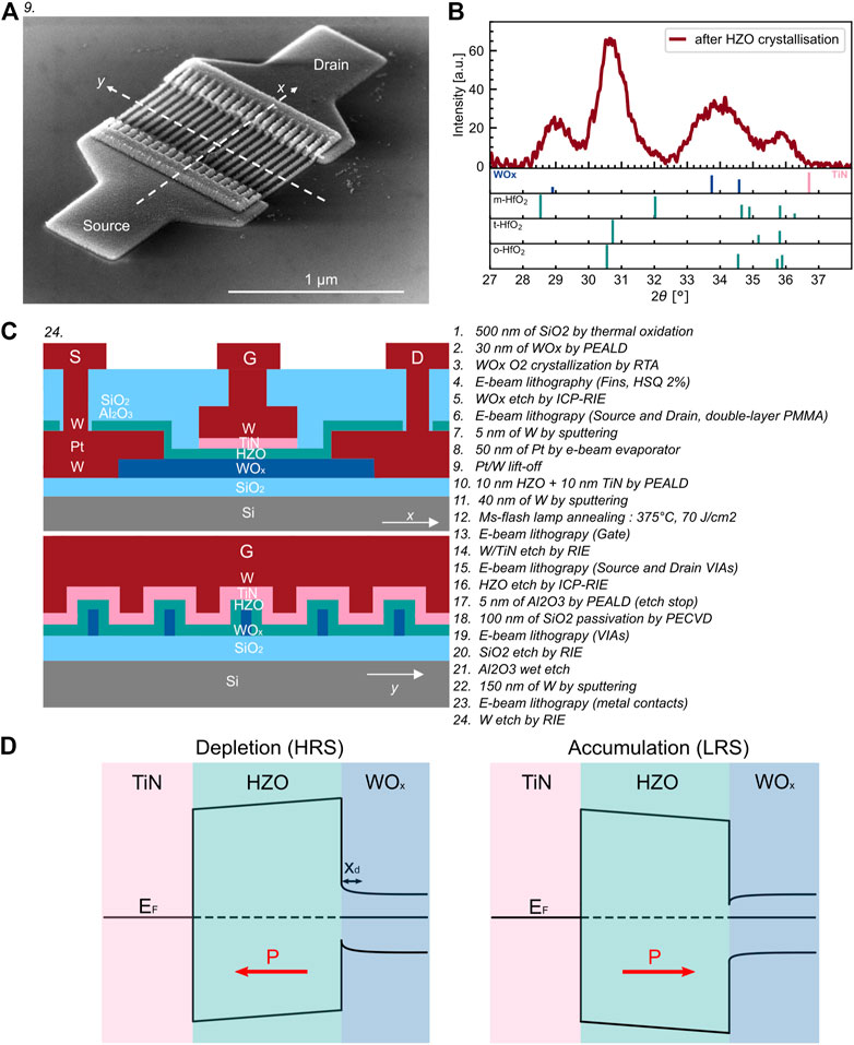
FIGURE 1. (A) SEM image after the source and drain contacts lift-off of a FinFeFET having L = 500 nm, N = 20 and W = 10 nm. (B) GIXRD for a diffraction angle (2θ) from 27° to 38° showing the presence of the characteristic peaks at 30.5° and 30.8° of the orthorhombic and tetragonal crystalline phases in HZO and the presence of the crystalline WOx. (C) The cross-section sketches of the FinFeFET after stage 24, and its relative process flow, are provided. (D) Schematic energy band diagrams in depletion (HRS) and accumulation (LRS) states.
Polarization charges are screened in the HRS state and it is possible to define a screening length (depletion width) xd, representing the thickness of the channel where the resistance is modulated. By decreasing the carrier density
where q is the elementary charge, μ the electron mobility, and
where ϵHZO is the permittivity of HZO, which for the ferroelectric phase is 29.1 (Materlik et al., 2015b). The depletion width xd in WOx with respect to the electric field caused by the polarization charges can be related by using Poisson’s equation Brotherton (2013):
By combining Eqs 2, 3, the depletion width can be estimated as follows:
where
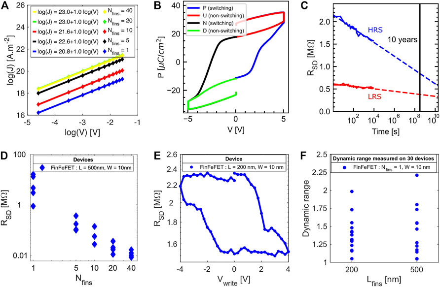
FIGURE 2. (A) Ohmic conduction in the WOx channel of FinFeFETs. (B) Positive-Up Negative-Down (PUND) measurements of a MSFM capacitor with an 40 µm2 × 40 µm2 area. (C) Retention measurements on a single-fin FinFeFET with Lfins = 500 nm and Wfins = 10 nm, at room temperature for 500 µs set/reset pulses. (D) Pristine channel resistance RSD as a function of the number of fins Nfins. (E) RSD after the application of a DC-voltage Vwrite of varying amplitude. Each data point corresponds to a resistance measurement between source and drain at Vread = 200 mV. (F) Dynamic range measured on 30 single-fin FinFeFETs with Lfins = 200 nm and Lfins = 500 nm.
Several pulsing schemes on HZO based FeFETs have been investigated in the past (Jerry et al., 2018). In this work, the scheme using pulses with varying amplitudes and constant width was used since it optimizes the number of accessible polarization states (Jerry et al., 2018). The analog nature of a representative FinFeFET (Figure 3A) having a 10 nm wide and 500 nm long fin, was explored by applying voltage pulses of varying amplitude Vwrite while keeping a fixed pulse duration of 5 µs. For the potentiation, Vwrite was increased from 1 to 5 V, and for the depression, decreased from −1 to −5.5 V, with 50 mV steps. A slightly higher voltage was used for the depression to compensate the built-in field in HZO. After each pulse, the channel resistance RSD was measured at Vread = 200 mV, keeping the gate floating. The memristor showed a HRS of ≃ 1 MΩ and a LRS of ≃ 0.7 MΩ (HRS/LRS ≃ 1.4). With respect to the DC-electrical characterization, almost all the devices had a decrease in dynamic range. This may be explained considering the short programming pulses and that the dynamics of ferroelectric switching in polycrystalline HZO films follow the Merz law (Chanthbouala et al., 2012), (Paruch et al., 2006), hence the coercive field (Ec) depends linearly on the logarithm of the writing time, as detailed for polycrystalline HZO devices in (Bégon-Lours et al., 2021). Another explanation could be an oxygen drift across the HZO—WOx interface, a much slower process than ferroelectric switching, that would lead to an oxidation/reduction of the WOx channel. The drift phenomena should be more pronounced in the DC potentiation and depression and thereby lead to the observed dynamic range dependence on the write signal length. The cycle to cycle variability was taken into account averaging all the potentiation and depression cycles (Figure 3B). By decreasing the range of Vwrite, the dynamic range is reduced. The number of the intermediate states is defined by the potentiation and depression step size, which can be further reduced to increase the resolution. The resistive states are not all differentiable, however the monotonic increasing and decreasing trends are desirable for online learning. The weight-update linearity was quantified by fitting the normalized weight update characteristics, by a function of the normalized pulse number, as proposed by (Chen et al., 2018b; Chen et al., 2018c):
The parameter A was chosen by minimizing the root mean square error of the fitting. Values of ALTP = 1.2 for the potentiation and ALTD = −2.5 for the depression, respectively, were found (see Figure 3C).
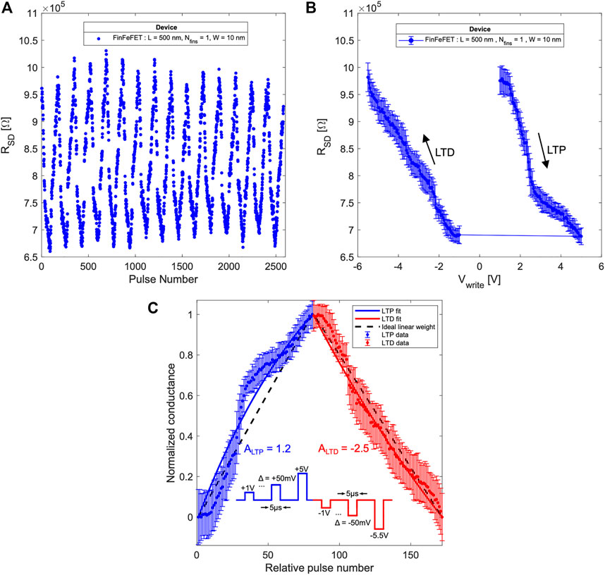
FIGURE 3. (A) Multiple potentiation and depression cycles of a representative FinFeFET. After each pulse, RSD is measured. (B) Channel resistance RSD averaged over 15 potentiation and depression cycles. (C) Experimental data and relative fits using the device behavioral model of the non-linear weight update provided by Chen et al. (2018b) and Chen et al. (2018c). The bottom insert details the pulsing scheme used.
Considering the ferroelectric synaptic weight dependence both on the pulse amplitude and duration, FinFeFETs are promising devices for Spike-Timing-Dependent Plasticity (STDP). However, STDP was not implemented with such devices in this work, since it requires tailored spike shapes as described by (Boyn et al., 2017) in ferroelectric perovskites and by (Max et al., 2020) in ferroelectric hafnia.
3 Conclusion
We developed a manufacturing process to allow the transfer and the scale-down of the FeFET planar technology into a multigate FinFeFET configuration. The fabrication process is compatible with the integration in the back end of line of CMOS technology and is using only abundant materials, making it suitable for large-scale integration. An Ohmic conduction in scaled WOx fins, as well as good retention, analog states and an almost symmetric and linear potentiation and depression were obtained. Future work will focus on controlling the carrier concentration of WOx fins, to further increase the resistance range and the dynamic range.
4 Experimental Section
4.1 Sample Fabrication
A 500 nm thick SiO2 was grown on Si by thermal oxidation. Then, 30 nm WOx was deposited using a (BuN)2W(NMe2)2 precursor and O2 plasma at T = 375°C in an Oxford Instruments Plasma-Enhanced Atomic Layer Deposition (PEALD) system. The crystallization and the oxidation of WOx to WO3 was performed in a Rapid Thermal Annealer (RTA) by O2-annealing at T = 350°C for 30min. The WO3 was then structured using an Inductively Coupled Plasma Reactive Ion Etcher (ICP-RIE) with SF6 plasma, and Hydrogen Silsesquioxane (HSQ) 2% as negative resist. The source and drain metal contacts were defined by lift-off using a double layer PMMA e-beam resist. 5 nm of W was first deposited by sputtering, then 50 nm of Pt was evaporated prior to the lift-off. An approximately 10 nm thick layer of HZO was grown in PEALD system through a process exploiting alternating cycles of tetrakis-(ethylmethylamino)hafnium (TEMAH) and bis(methyl-η5-cyclopentadienyl)methoxymethylzirconium (ZrCMMM) at T = 300°C. Then, further 10 nm of TiN were deposited using tetrakis-(dimethylamino)titanium (TDMAT) as precursor and N2/H2 plasma in a PEALD system. The sample was then immediately transferred to a sputter chamber for the deposition of 40 nm W as gate electrode. Millisecond flash lamp annealing (O’Connor et al., 2018), with a background temperature of 375°C and a flash energy density of 70 J/cm2, was performed to crystallize HZO. The patterning of the gate electrode was achieved using a Reactive Ion Etcher (RIE) with SF6 plasma. Source and drain vias were etched through the HZO by ICP-RIE with CHF3/O2 plasma. The passivation consists of 5 nm Al2O3 by PEALD using trimethylaluminum (TMA) as precursor and 100 nm SiO2 by plasma-enhanced chemical vapor deposition (PECVD). Vias were etched using an RIE with a CHF3/O2 plasma. Al2O3, used as etch stop layer during SiO2 etching, was then removed by a wet etching in MIF726 developer. Finally, the contacts were realized by depositing 150 nm W by sputtering and defined in a RIE with an SF6/O2 plasma.
4.2 Structural Characterization
Grazing-Incidence X-Ray Diffraction (GIXRD) measurements were performed by a Bruker D8 Discover diffractometer equipped with a rotating Cu anode generator. The Scanning Electron Microscope (SEM) system used in this work is the FEI Helios NanoLab 450S.
4.3 Electrical Characterization
The PUND measurements were performed on a TF2000 ferroelectric analyzer from aixACCT with a frequency of 1 kHz on capacitors with an area of 40 µm2 × 40 µm2. Prior to the PUND measurement, bipolar cycling stress with an AC amplitude of 3.5 V and frequency of 1 kHz for 103 cycles was applied to wake-up the HZO. The DC and the pulsed electrical characterization of the memristors were performed using an Agilent B1500A semiconductor device analyzer. Before the DC characterization of the dynamic range, a wake-up procedure of the HZO with 100 cycles of ±4 V was applied. Set (reset) of the FinFeFETs was obtained by applying a positive (negative) DC bias of decreasing (increasing) amplitude on the gate, keeping the source and drain electrodes grounded. After the application of each bias (whose duration was not controlled) of amplitude Vwrite (that varies in the −4 to 4 V range) the channel resistance was measured at Vread = 200 mV, keeping the gate floating. During the pulsed characterization, Vwrite pulses were generated by a Waveform Generator Fast Measurement Unit (WGFMU) of a Agilent B1500A, and applied directly to the gate through a triax cable, while grounding both the source and the drain. After each pulse, the channel resistance RSD was measured, keeping the gate floating and applying a voltage sweep from −200 to 200 mV along the channel. RSD was then determined by reading the resistance at 200 mV.
Data Availability Statement
The raw data supporting the conclusion of this article will be made available by the authors, without undue reservation.
Author Contributions
DF has contributed with the fabrication, the electrical measurements and interpretation of the results as well as with the writing of the manuscript. MH initiated the project and contributed with the fabrication, the design and technical guidance, with the interpretation of the data and revision of the manuscript. LB-L and BO have contributed with the interpretation of the data and manuscript revision.
Funding
This work is funded by H2020 FREEMIND (No. 840903), ULPEC (No. 732642), BeFerroSynaptic (No. 871737) and CHIST-ERA, UNICO (No. 20CH21-186952).
Conflict of Interest
DFF, LB-L and BJO were employed by the company IBM Research Europe.
The remaining author declares that the research was conducted in the absence of any commercial or financial relationships that could be construed as a potential conflict of interest.
Publisher’s Note
All claims expressed in this article are solely those of the authors and do not necessarily represent those of their affiliated organizations, or those of the publisher, the editors and the reviewers. Any product that may be evaluated in this article, or claim that may be made by its manufacturer, is not guaranteed or endorsed by the publisher.
Acknowledgments
The authors acknowledge the support of the operation team of the Binnig and Rohrer Nanotechnology Center (BRNC), especially Antonis Olziersky for the optimization of the e-beam lithographic processes.
References
Ambriz-Vargas, F., Kolhatkar, G., Broyer, M., Hadj-Youssef, A., Nouar, R., Sarkissian, A., et al. (2017). A Complementary Metal Oxide Semiconductor Process-Compatible Ferroelectric Tunnel junction. ACS Appl. Mater. Inter. 9, 13262–13268. doi:10.1021/acsami.6b16173
Baek, I. G., Lee, M. S., Sco, S., Lee, M. J., Seo, D. H., Suh, D.-S., et al. (2004). Highly Scalable Non-volatile Resistive Memory Using Simple Binary Oxide Driven by Asymmetric Unipolar Voltage Pulses. Tech. Dig. - Int. Electron Devices Meet. IEDM. doi:10.1109/iedm.2004.1419228
Begon-Lours, L., Halter, M., Popoff, Y., Yu, Z., Falcone, D. F., Davila, D., et al. (2021). Analog Resistive Switching in Beol, Ferroelectric Synaptic Weights. IEEE J. Electron. Devices Soc. 9, 1275–1281. doi:10.1109/JEDS.2021.3108523
Bégon-Lours, L., Halter, M., Popoff, Y., Yu, Z., Falcone, D. F., and Offrein, B. J. (2021). “High-Conductance, Ohmic-like HfZrO4 Ferroelectric Memristor,” in ESSDERC 2021 - IEEE 51st European Solid-State Device Research Conference (ESSDERC), 87–90. doi:10.1109/ESSCIRC53450.2021.9567870
Bégon-Lours, L., Rouco, V., Qiao, Q., Sander, A., Roldán, M. A., Bernard, R., et al. (2018). Factors Limiting Ferroelectric Field-Effect Doping in Complex Oxide Heterostructures. Phys. Rev. Mater. 2. doi:10.1103/PhysRevMaterials.2.084405
Böscke, T. S., Müller, J., Brauhaus, D., Schroder, U., and Bottger, U. (2011). “Ferroelectricity in Hafnium Oxide: Cmos Compatible Ferroelectric Field Effect Transistors,” in Electron Devices Meeting, 1988. IEDM ’88. Technical Digest., International, 24.5.1–24.5.4. doi:10.1109/IEDM.2011.613160699
Boybat, I., Le Gallo, M., Nandakumar, S. R., Moraitis, T., Parnell, T., Tuma, T., et al. (2018). Neuromorphic Computing with Multi-Memristive Synapses. Nat. Commun. 9. doi:10.1038/s41467-018-04933-y
Boyn, S., Grollier, J., Lecerf, G., Xu, B., Locatelli, N., Fusil, S., et al. (2017). Learning through Ferroelectric Domain Dynamics in Solid-State Synapses. Nat. Commun. 8. doi:10.1038/ncomms14736
Chanthbouala, A., Garcia, V., Cherifi, R. O., Bouzehouane, K., Fusil, S., Moya, X., et al. (2012). A Ferroelectric Memristor. Nat. Mater 11, 860–864. doi:10.1038/nmat3415
Chen, L., Wang, T.-Y., Dai, Y.-W., Cha, M.-Y., Zhu, H., Sun, Q.-Q., et al. (2018a). Ultra-low Power hf0.5zr0.5o2 Based Ferroelectric Tunnel junction Synapses for Hardware Neural Network Applications. Nanoscale 10, 15826–15833. doi:10.1039/c8nr04734k
Chen, P.-Y., Peng, X., and Yu, S. (2017c). “Neurosim+: An Integrated Device-To-Algorithm Framework for Benchmarking Synaptic Devices and Array Architectures,” in International Electron Devices Meeting, IEDM. doi:10.1109/IEDM.2017.8268337
Chen, P.-Y., Peng, X., and Yu, S. (2018b). Neurosim: A Circuit-Level Macro Model for Benchmarking Neuro-Inspired Architectures in Online Learning. IEEE Trans. Comput.-Aided Des. Integr. Circuits Syst. 37, 3067–3080. doi:10.1109/TCAD.2018.2789723
Cheng, S., Fan, Z., Rao, J., Hong, L., Huang, Q., Tao, R., et al. (2020). Highly Controllable and Silicon-Compatible Ferroelectric Photovoltaic Synapses for Neuromorphic Computing. iScience 23, 101874. doi:10.1016/j.isci.2020.101874
Colinge, J.-P., Lee, C.-W., Afzalian, A., Akhavan, N. D., Yan, R., Ferain, I., et al. (2010). Nanowire Transistors without Junctions. Nat. Nanotech 5, 225–229. doi:10.1038/nnano.2010.15
Colinge, J. P., Kranti, A., Yan, R., Lee, C. W., Ferain, I., Yu, R., et al. (2011). Junctionless Nanowire Transistor (JNT): Properties and Design Guidelines. Solid-State Elect. 65-66, 33–37. doi:10.1016/j.sse.2011.06.004
Cui, B., Fan, Z., Li, W., Chen, Y., Dong, S., Tan, Z., et al. (2021). Ferroelectric Photosensor Network: an Advanced Hardware Solution to Real-Time Machine Vision doi:10.21203/rs.3.rs-969097/v1
Davis, D. (1973). Thomas-fermi Screening in One Dimension. Phys. Rev. B 7, 129–135. doi:10.1103/PhysRevB.7.129
Fuller, E. J., Gabaly, F. E., Léonard, F., Agarwal, S., Plimpton, S. J., Jacobs‐Gedrim, R. B., et al. (2017). Li‐Ion Synaptic Transistor for Low Power Analog Computing. Adv. Mater. 29, 1604310. doi:10.1002/adma.201604310
Goh, Y., and Jeon, S. (2018). The Effect of the Bottom Electrode on Ferroelectric Tunnel Junctions Based on Cmos-Compatible Hfo2. Nanotechnology 29, 335201. doi:10.1088/1361-6528/aac6b3
Gokmen, T., and Vlasov, Y. (2016). Acceleration of Deep Neural Network Training with Resistive Cross-point Devices: Design Considerations. Front. Neurosci. 10, 333. doi:10.3389/fnins.2016.00333
Gokmen, T., Vlasov, Y., and Yurii, (2016). Acceleration of Deep Neural Network Training with Resistive Cross-point Devices: Design Considerations. Front. Neurosci. 10. doi:10.3389/fnins.2016.00333
Guo, R., You, L., Zhou, Y., Shiuh Lim, Z., Zou, X., Chen, L., et al. (2013). Non-volatile Memory Based on the Ferroelectric Photovoltaic Effect. Nat. Commun. 4. doi:10.1038/ncomms2990
Guo, R., Zhou, Y., Wu, L., Wang, Z., Lim, Z., Yan, X., et al. (2018). Control of Synaptic Plasticity Learning of Ferroelectric Tunnel Memristor by Nanoscale Interface Engineering. ACS Appl. Mater. Inter. 10, 12862–12869. doi:10.1021/acsami.8b01469
Halter, M., Bégon-Lours, L., Bragaglia, V., Sousa, M., Offrein, B. J., Abel, S., et al. (2020). Back-end, Cmos-Compatible Ferroelectric Field-Effect Transistor for Synaptic Weights. ACS Appl. Mater. Inter. 12, 17725–17732. doi:10.1021/acsami.0c00877
Hyuk Park, M., Joon Kim, H., Jin Kim, Y., Lee, W., Moon, T., and Seong Hwang, C. (2013). Evolution of Phases and Ferroelectric Properties of Thin Hf0.5Zr0.5O2 Films According to the Thickness and Annealing Temperature. Appl. Phys. Lett. 102, 242905. doi:10.1063/1.4811483
Jain, A., Ong, S. P., Hautier, G., Chen, W., Richards, W. D., Dacek, S., et al. (2013). Commentary: The Materials Project: A Materials Genome Approach to Accelerating Materials Innovation. APL Mater. 1, 011002. doi:10.1063/1.4812323
Jerry, M., Chen, P. Y., Zhang, J., Sharma, P., Ni, K., Yu, S., et al. (2018). “Ferroelectric Fet Analog Synapse for Acceleration of Deep Neural Network Training,” in Technical Digest - International Electron Devices Meeting, IEDM. doi:10.1109/IEDM.2017.8268338
Kim, S., Gokmen, T., Lee, H.-M., and Haensch, W. E. (2017). “Analog Cmos-Based Resistive Processing Unit for Deep Neural Network Training,” in Midwest Symposium on Circuits and Systems, 2017-August. doi:10.1109/MWSCAS.2017.8052950
Kim, S., Todorov, T., Onen, M., Gokmen, T., Bishop, D., Solomon, P., et al. (2019). “Metal-oxide Based, Cmos-Compatible Ecram for Deep Learning Accelerator,” in Technical Digest - International Electron Devices Meeting, IEDM, 2019-December. doi:10.1109/IEDM19573.2019.8993463
Krivokapic, Z., Rana, U., Galatage, R., Razavieh, A., Aziz, A., Liu, J., et al. (2017). “14nm Ferroelectric Finfet Technology with Steep Subthreshold Slope for Ultra Low Power Applications,” in Technical Digest - International Electron Devices Meeting, IEDM. doi:10.1109/IEDM.2017.8268393
Lacaita, A. L. (2006). Phase Change Memories: State-Of-The-Art, Challenges and Perspectives. Solid-State Elect. 50, 24–31. doi:10.1016/j.sse.2005.10.046
Lawrence, B., and Rubia, J. (2015). “Review of Fin Fet Technology and Circuit Design Challenges,” in Journal of Engineering Research and Applications. www.ijera.com 5.
Lee, H. Y., Chen, P. S., Wu, T. Y., Chen, Y. S., Wang, C. C., Tzeng, P. J., et al. (2008). “Low Power and High Speed Bipolar Switching with a Thin Reactive Ti Buffer Layer in Robust Hfo2 Based Rram,” in Technical Digest - International Electron Devices Meeting, IEDM. doi:10.1109/IEDM.2008.4796677
Li, J., Ge, C., Du, J., Wang, C., Yang, G., and Jin, K. (2020). Reproducible Ultrathin Ferroelectric Domain Switching for High‐Performance Neuromorphic Computing. Adv. Mater. 32, 1905764. doi:10.1002/adma.201905764
Majumdar, S., Tan, H., Qin, Q. H., and van Dijken, S. (2019). Energy-efficient Organic Ferroelectric Tunnel junction Memristors for Neuromorphic Computing. Adv. Electron. Mater. 5, 1800795. doi:10.1002/aelm.201800795
Materlik, R., Künneth, C., and Kersch, A. (2015a). The Origin of Ferroelectricity in Hf1−xZrxO2: A Computational Investigation and a Surface Energy Model. J. Appl. Phys. 117, 134109. doi:10.1063/1.4916707
Materlik, R., Künneth, C., and Kersch, A. (2015b). The Origin of Ferroelectricity in Hf1−xZrxO2: A Computational Investigation and a Surface Energy Model. J. Appl. Phys. 117, 134109. doi:10.1063/1.4916707
Max, B., Hoffmann, M., Mulaosmanovic, H., Slesazeck, S., and Mikolajick, T. (2020). Hafnia-based Double-Layer Ferroelectric Tunnel Junctions as Artificial Synapses for Neuromorphic Computing. ACS Appl. Electron. Mater. 2, 4023–4033. doi:10.1021/acsaelm.0c00832
Mehta, R. R., Silverman, B. D., and Jacobs, J. T. (1973). Depolarization fields in Thin Ferroelectric Films. J. Appl. Phys. 44, 3379–3385. doi:10.1063/1.1662770
Mo, F., Tagawa, Y., Jin, C., Ahn, M., Saraya, T., Hiramoto, T., et al. (2019). “Experimental Demonstration of Ferroelectric Hfo2 Fet with Ultrathin-Body Igzo for High-Density and Low-Power Memory Application,” in Digest of Technical Papers - Symposium on VLSI Technology, 2019-June. doi:10.23919/VLSIT.2019.8776553
Mulaosmanovic, H., Chicca, E., Bertele, M., Mikolajick, T., and Slesazeck, S. (2018). Mimicking Biological Neurons with a Nanoscale Ferroelectric Transistor. Nanoscale 10, 21755–21763. doi:10.1039/C8NR07135G
Mulaosmanovic, H., Ocker, J., Müller, S., Schroeder, U., Müller, J., Polakowski, P., et al. (2017). Switching Kinetics in Nanoscale Hafnium Oxide Based Ferroelectric Field-Effect Transistors. ACS Appl. Mater. Inter. 9, 3792–3798. doi:10.1021/acsami.6b13866
Nishitani, Y., Kaneko, Y., Ueda, M., Morie, T., and Fujii, E. (2012). Three-terminal Ferroelectric Synapse Device with Concurrent Learning Function for Artificial Neural Networks. J. Appl. Phys. 111, 124108. doi:10.1063/1.4729915
O’Connor, É., Halter, M., Eltes, F., Sousa, M., Kellock, A., Abel, S., et al. (2018). Stabilization of Ferroelectric HfxZr1−xO2 Films Using a Millisecond Flash Lamp Annealing Technique. APL Mater. 6, 121103. doi:10.1063/1.5060676
Paruch, P., Giamarchi, T., Tybell, T., and Triscone, J.-M. (2006). Nanoscale Studies of Domain wall Motion in Epitaxial Ferroelectric Thin Films. J. Appl. Phys. 100, 051608. doi:10.1063/1.2337356
Poon, C.-S., and Zhou, K. (2011). Neuromorphic Silicon Neurons and Large-Scale Neural Networks: Challenges and Opportunities. Front. Neurosci. 5. doi:10.3389/fnins.2011.00108
Raoux, S., Wełnic, W., and Ielmini, D. (2010). Phase Change Materials and Their Application to Nonvolatile Memories. Chem. Rev. 110, 240–267. doi:10.1021/cr900040x
Salje, E., and Güttler, B. (1984). Anderson Transition and Intermediate Polaron Formation in WO3-xTransport Properties and Optical Absorption. Philosophical Mag. B 50, 607–620. doi:10.1080/13642818408238882
Sharma, P., Tapily, K., Saha, A. K., Zhang, J., Shaughnessy, A., Aziz, A., et al. (2017). “Impact of Total and Partial Dipole Switching on the Switching Slope of Gate-Last Negative Capacitance Fets with Ferroelectric Hafnium Zirconium Oxide Gate Stack,” in Digest of Technical Papers - Symposium on VLSI Technology. doi:10.23919/VLSIT.2017.7998160
Tang, J., Bishop, D., Kim, S., Copel, M., Gokmen, T., Todorov, T., et al. (2018). “Ecram as Scalable Synaptic Cell for High-Speed, Low-Power Neuromorphic Computing,” in Technical Digest - International Electron Devices Meeting, 2018-December (IEDM). doi:10.1109/IEDM.2018.8614551
Tian, X., and Toriumi, A. (2017). “New Opportunity of Ferroelectric Tunnel junction Memory with Ultrathin Hfo2-Based Oxides,” in 2017 IEEE Electron Devices Technology and Manufacturing Conference, EDTM 2017 - Proceedings. doi:10.1109/EDTM.2017.7947507
Waser, R., Dittmann, R., Staikov, G., and Szot, K. (2009). Redox-Based Resistive Switching Memories - Nanoionic Mechanisms, Prospects, and Challenges. Adv. Mater. 21, 2632–2663. doi:10.1002/adma.200900375
Wong, H.-S. P., and Salahuddin, S. (2015). Memory Leads the Way to Better Computing. Nat. Nanotech 10, 191–194. doi:10.1038/nnano.2015.29
Yu, S. (2018). Neuro-inspired Computing with Emerging Nonvolatile Memorys. Proc. IEEE 106, 260–285. doi:10.1109/JPROC.2018.2790840
Yu, T., He, F., Zhao, J., Zhou, Z., Chang, J., Chen, J., et al. (2021). Hf0.5zr0.5o2-based Ferroelectric Memristor with Multilevel Storage Potential and Artificial Synaptic Plasticity. Sci. China Mater. 64, 727–738. doi:10.1007/s40843-020-1444-1
Keywords: ferroelectric switching, hafnium zirconium oxide, tungsten oxide, back-end-of-line compatible, ferroelectric fin field effect transistor, memristors, neuromorphic computing, synapse
Citation: Falcone DF, Halter M, Bégon-Lours L and Offrein BJ (2022) Back-End, CMOS-Compatible Ferroelectric FinFET for Synaptic Weights. Front. Electron. Mater. 2:849879. doi: 10.3389/femat.2022.849879
Received: 06 January 2022; Accepted: 23 March 2022;
Published: 19 April 2022.
Edited by:
Kai Ni, Rochester Institute of Technology, United StatesReviewed by:
Zhen Fan, South China Normal University, ChinaK. B. Jinesh, Indian Institute of Space Science and Technology, India
Copyright © 2022 Falcone, Halter, Bégon-Lours and Offrein. This is an open-access article distributed under the terms of the Creative Commons Attribution License (CC BY). The use, distribution or reproduction in other forums is permitted, provided the original author(s) and the copyright owner(s) are credited and that the original publication in this journal is cited, in accordance with accepted academic practice. No use, distribution or reproduction is permitted which does not comply with these terms.
*Correspondence: Donato Francesco Falcone, ZG9mQHp1cmljaC5pYm0uY29t
†These authors have contributed equally to this work and share first authorship