This article is part of the Research TopicMemristive Neuromorphics: Materials, Devices, Circuits, Architectures, Algorithms and their Co-DesignView all 13 articles
System-Theoretic Methods for Designing Bio-Inspired Mem-Computing Memristor Cellular Nonlinear Networks
1Fundamentals of Electrical Engineering, Institute of Circuits and Systems, Faculty of Electrical and Computer Engineering, Technische Universität, Dresden, Germany
2Department of Microelectronics, Brno University of Technology, Brno, Czech Republic
3Department of Electrical and Computer Engineering, University of California Santa Cruz, Santa Cruz, CA, United States
4Department of Electrical Engineering and Computer Sciences, University of California Berkeley, Berkeley, CA, United States
The introduction of nano-memristors in electronics may allow to boost the performance of integrated circuits beyond the Moore era, especially in view of their extraordinary capability to process and store data in the very same physical volume. However, recurring to nonlinear system theory is absolutely necessary for the development of a systematic approach to memristive circuit design. In fact, the application of linear system-theoretic techniques is not suitable to explore thoroughly the rich dynamics of resistance switching memories, and designing circuits without a comprehensive picture of the nonlinear behaviour of these devices may lead to the realization of technical systems failing to operate as desired. Converting traditional circuits to memristive equivalents may require the adaptation of classical methods from nonlinear system theory. This paper extends the theory of time- and space-invariant standard cellular nonlinear networks with first-order processing elements for the case where a single non-volatile memristor is inserted in parallel to the capacitor in each cell. A novel nonlinear system-theoretic method allows to draw a comprehensive picture of the dynamical phenomena emerging in the memristive mem-computing array, beautifully illustrated in the so-called Primary Mosaic for the class of uncoupled memristor cellular nonlinear networks. Employing this new analysis tool it is possible to elucidate, with the support of illustrative examples, how to design variability-tolerant bio-inspired cellular nonlinear networks with second-order memristive cells for the execution of computing tasks or of memory operations. The capability of the class of memristor cellular nonlinear networks under focus to store and process information locally, without the need to insert additional memory units in each cell, may allow to increase considerably the spatial resolution of state-of-the-art purely CMOS sensor-processor arrays. This is of great appeal for edge computing applications, especially since the Internet-of-Things industry is currently calling for the realization of miniaturized, lightweight, low-power, and high-speed mem-computers with sensing capability on board.
1 Introduction
On August 28th, 2018 GlobalFoundries announced to halt the 7 nm chip development. After installing at least one Extreme-Ultraviolet Lithography (EUV) machine at one of its fabs, the foundry reckoned there would not be enough customers, interested in the cutting-edge 7 nm node technology process, to make chip development profitable (GlobalFoundries Ltd, 2018). Despite Intel, Samsung, and TSMC are still making efforts to reduce the size of integrated circuits (ICs) further, transistor scaling is approaching atomic boundaries, with an inevitable concurrent rise in manufacturing costs. This issue is known as Moore wall. With the Moore era (Moore, 1965) coming to a natural end (Williams, 2017), a great deal of resources have been deployed over the past decade toward the development of innovative disruptive nanotechnologies, which may enable the development of versatile multi-functional devices, that, opening the door toward the implementation of peculiar signal processing paradigms, would allow to boost the performance of conventional circuits and systems without the need to shrink the size of transistors any further. Two are the factors for the inefficiency of machines based upon the von Neumann architecture: 1) There is a large mismatch between processing time and shuttling time. This issue is known as memory wall or von Neumann bottleneck. 2) The energy dissipated by digital switching units is no longer following the exponentially decreasing trend, predicted by Landauer (Landauer, 1988), with the reduction in IC dimensions. This issue, known as heat wall, poses serious risks for the lifetime of transistors. Memristors (Chua, 1971; Chua and Kang, 1976) represent one of the most promising nanotechnologies to address the problems affecting state-of-the-art electronics. A current (voltage)-controlled non-volatile memristor (Chua, 2014; Chua, 2015) is a two-terminal device, whose resistance (conductance) can be tuned to some desired value by applying a current (voltage) signal through (across) it, and which remembers its resistance (conductance) after the current (voltage) source, in parallel to it, is disconnected (Chua, 2018a). It remembers its past! (Chua, 2018b). The most impressive and peculiar virtue of non-volatile memristors is the combined capability to store data, thanks to excellent data retention levels, achievable without the need for external batteries, and to process signals, through the rich nonlinear dynamics of the memory state, within a single nano-scale volume, which enables the implementation of in-memory computing and mem-computing paradigms1, mimicking the distributed nature of memory and processing operations in the human brain, in future computing machines. Other distinctive qualities of memristors are low-power and high-speed operation, superior endurance, and, very importantly, good compatibility with CMOS technology. While in conventional memories data are stored as voltage levels, in memristors the physical quantity, which holds the information content, is the resistance. Given that all nonvolatile memories based upon resistance switching phenomena, irrespective of their constitutive materials and operating principles, are memristors (Chua, 2011), a wide range of nanotechnologies, including Resistive Random Access Memories (ReRAMs), Phase Change Memories (PCMs), Magnetic Tunnel Junctions (MTJs), Spin-Transfer-Torque Magneto-Resistive Random Access Memories (STTM-RRAMs), and Ferroelectric Tunnel Junctions (FTJs), are competing one with the other to produce the best performing data storage device for future brain-like computers. While many people believe that non-volatile nano-memristors will eventually replace conventional memories, including Flash Memories, Dynamic RAMs (DRAMs), and Hard Disk Drives (HDDs), the aforementioned nanotechnologies are not yet mature enough to draw conclusions on the portion of the nonvolatile memory market, which memristors will be able to cover in the next five years from now. However, edge computing technical systems already make use of memristive memories. Panasonic (Panasonic Ltd., 2013) have been launching mass production of micro-computers with 64 kB ReRAM-based data storage for battery-powered equipment, including portable devices for medical, healthcare, and security applications already in 2013, while Fujitsu (Fujitsu Ltd, 2019) has recently taken a step forward by offering 1024 kB ReRAMs for wearable units–e.g., smart watches and glasses–and hearing aids. Even when used simply as tunable resistors, memristors offer unique opportunities to enhance the performance of conventional data processing systems. Most computing tasks in artificial intelligence (AI) applications consist of machine-learning operations, such as object, image, and speech recognition, which require the calculation of a massive number of vector-matrix multiplications (VMMs). Nowadays these calculations are executed through expensive and bulky supercomputers. But with the advent of the memristor, which, leveraging Ohm’s law, naturally carries out a multiplication operation between the conductance it holds and the voltage falling between its terminals, outputting the result into the current flowing through it, it is possible to use a crossbar array (Li et al., 2018) to compute at unprecedented rates the product between a vector of voltages, distributed along the rows, and a matrix of memristor crosspoint conductances, with the computation result available in current form along the columns (refer to the Dot Product Engine (DPE) lab prototype developed at Hewlett Packard Enterprise (Hu et al., 2016)). Last but not least, given that the two constitutive elements of the human brain, namely the synapse and the neuron, are made of nonvolatile and volatile memristors, respectively, resistance switching memories allow to develop innovative neuromorphic circuits, which promise to outperform conventional purely CMOS counterparts in mimicking the functionalities of the human brain. Non-volatile memristor devices, in which the resistance may be finely tuned under excitation, may reproduce most closely the plastic response of biological synapses to external stimuli. Furthermore, there exist a large class of memristor physical nano-scale realisations, which, despite being unable to store data–for this reason they are classified as volatile memories –, feature the extraordinary capability to amplify infinitesimal fluctuations in energy (Bohaichuk et al., 2019; Kumar et al., 2020), a property which is referred to as local activity (Chua, 2005), and which enables the development of realistic electronic realisations of spiking neurons2 (Chua et al., 2012), the so-called neuristors.
Besides constitutive the ideal framework for modeling biological systems (Chua, 1998; Chua and Roska, 2002), Cellular Nonlinear Networks (CNNs) (Chua and Yang, 1988a; Chua and Yang, 1988b) represent a powerful multi-variate signal processing paradigm, which, featuring a bio-inspired architecture, operates in a massively parallel fashion, allowing to process data at very high rates, as necessary in time-critical Internet-of-Things (IoT) applications, nowadays. Purely CMOS analogue hardware implementations of the CNN signal processing paradigm are typically co-integrated with highly selective equal-sized sensor arrays to allow the solution of complex computing tasks directly where the acquisition of specific data takes place (Vázquez et al., 2018). A technological issue, which limits the applicability scope of these sensor-processor arrays, is related to the huge difference between the typically small minimum size of an element of the sensor matrix, and the relatively large minimum integrated circuit (IC) area, which a processing element of the CNN hardware realization usually occupies, due to the fact that it needs to accommodate memory units, which endow the resulting computing machine with local stored programmability on board, allowing to harness thoroughly the advantages associated with the massive parallelism of the CNN signal processing paradigm. The adoption of non-volatile memristors (Chua, 2015), capable to combine data processing and storage functionalities within a common nanoscale physical volume, in CNN circuit design may allow to increase significantly the spatial resolution of the cellular computing machine. Moreover, leveraging the rich nonlinear dynamics of resistance switching memories, the computing capabilities of the processing elements of a memristive CNN hardware implementation (Duan et al., 2015; Di Marco et al., 2017a; Di Marco et al., 2017b; Di Marco et al., 2018) may be extended beyond the operational boundaries of the cells of a traditional purely CMOS implementation.
CNNs process information through the analogue dynamics of the cells’ states, which converge toward distinct attractors depending upon inputs and/or initial conditions. While wave-based computing, where the cellular array carries out data processing tasks through the generation of specific dynamic patterns, is an active field of research (Weiher et al., 2019), there exists a huge library (Karacs et al., 2018) of image processing operations, which the nonlinear dynamic array may execute as the cells’ states approach predefined equilibria. This paper focuses on the performance of CNNs (M-CNNs) as equilibria-based computing (mem-computing) engine. Now, for a full exploration of the potential of memristors in electronics, recurring to concepts from nonlinear system theory is necessary. In fact, linear system-theoretic methods are not suitable for the analysis and design of memristor-based circuits. However, as is the case here, converting traditional nonlinear circuits to memristive equivalents may require the extension of classical nonlinear system-theoretic techniques. The Memristor Cellular Nonlinear Network (M-CNN), proposed in Tetzlaff et al. (2020), differs from a standard time- and space-invariant two-dimensional CNN (Chua and Yang, 1988a; Chua and Yang, 1988b), characterized by first-order cells, and typically implemented in hardware (Vázquez et al., 2018), for the inclusion of a single non-volatile memristor in parallel to the capacitor in the circuit implementation of each processing element. One of the most powerful tools for the analysis of nonlinear dynamical systems with one degree of freedom is the Dynamic Route Map (DRM) (Chua, 2018a), which represents the system-theoretic technique of reference for the investigation of CNNs with first-order processing elements. Since the memristive cell in the proposed M-CNN features two degrees of freedom, the investigation of the cellular array calls for the generalization of the DRM graphical tool, applicable to first-order systems only. The modified DRM graphical tool, applicable to second-order dynamical systems, is known as Second-Order Dynamic Route Map (DRM2) (Tetzlaff et al., 2020). The application of this novel system-theoretic technique to the model of the proposed M-CNN allows to gain a deep insight into the rich nonlinear behaviour of its second-order processing elements, unveiling dynamical phenomena, which may not emerge in the original cellular array (Ascoli et al., 2020b). The DRM2 graphical tool lies at the basis of a systematic methodology to design variability-tolerant mem-computing arrays with second-order memristive cells (Ascoli et al., 2020a).
The structure of the paper is organized as follows. Section 2 revisits the theory of CNNs, explaining the invaluable role of the classical DRM graphical technique to analyze standard arrays of locally coupled processing elements, and elucidating through an illustrative example the traditional method, based upon this system-theoretic tool, to program the cellular computing engine for the execution of a predefined image processing task. Section 3 first defines the class of M-CNNs under study, including the model of the non-volatile memristor hosted in each cell, secondly extends the DRM graphical tool to second-order dynamical systems, elucidates how this allows to draw a comprehensive picture of the nonlinear dynamics of each memristive processing element, and finally presents a rigorous procedure, based upon the DRM2 system-theoretic technique, to design cellular mem-computing structures with second-order memristive cells. Sections 4 and 5 are devoted to the application of the M-CNN design methodology for operating the multifunctional memristive cellular computing engine as image processing system and as memory bank, respectively. A brief discussion, summarizing the significance of the research work, is provided in section 6. Conclusions are finally drafted in section 7.
2 Analysis and Design of Memristor Cellular Nonlinear Networks
Cellular Nonlinear Networks (CNNs) constitute a bio-inspired multivariate signal processing paradigm, which, based upon a massively parallel information flow, enables computations at very high rates, and is amenable to a Very Large Scale Integration (VLSI) circuit realization, which, centered around a non-von-Neumann machine architecture, enables computational universality. Introducing memristive devices in CNN VLSI design may provide two main benefits. Firstly, the rich spectrum of nonlinear dynamic phenomena, appearing in resistance switching memories, may simplify or extend the functionalities of traditional CNNs. Secondly, the unique combined capability of nonvolatile memristors to compute and store data within the same nanoscale physical medium may render unnecessary the need to include spacious data storage units within the circuit implementation of each cell, allowing to improve considerably the number of processing elements fitting into the IC design area allocated to the non-von-Neumann computing machine.
2.1 Theory of Cellular Nonlinear Networks
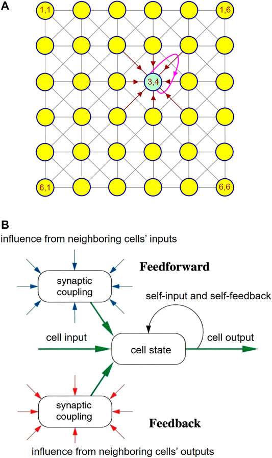
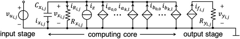
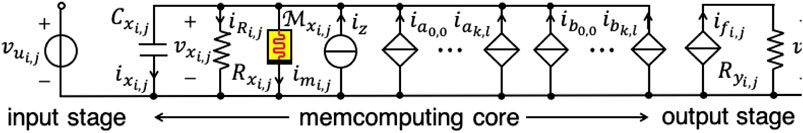
The theoretical foundations of CNNs were laid in 1988 by L. Chua (Chua and Yang, 1988a; Chua and Yang, 1988b). In the most general case, a CNN consists of a spatially discrete collection of locally coupled kth-order continuous-time processing elements, called cells, arranged at regular positions within a l-dimensional lattice. The architecture of a small two-dimensional CNN with M = 6 rows and N = 6 columns is presented in Figure 1A, under the assumption that each cell – , – is physically coupled to its 8 adjacent neighbors only3. Each cell is assigned a state, an input, an output, as well as a threshold. The rate of change of the state of a cell is influenced by the inputs and outputs of its 8 adjacent neighbors, as well as by its own input and output, as respectively sketched through eight brown directed segments and through one magenta directed loop in Figure 1A for the processing element located where the 3rd row crosses the 4th column. The block diagram in plot (b) of Figure 1 illustrates once more the key factors affecting the dynamical behaviour of a CNN cell. The neighbors’ inputs (outputs) are modulated by feedforward (feedback) synaptic weights before accessing the cell to affect the time evolution of its state, similarly as it occurs in biological neural networks. The cell of a standard time- and space-invariant two-dimensional CNN (Chua and Roska, 2002) is implemented by the circuit of Figure 2, where the computing core is mathematically described by4 (, )
in case it is physically coupled to its 8 adjacent neighbors only5 i.e., r = 1. With reference to the circuit of Figure 2, the main physical quantity within the input stage, the computing core, and the output stage respectively are the input voltage , the voltage across a capacitor with capacitance , expressing the state, and the output voltage . Focusing on the output stage, the latter physical quantity is defined as
where is the resistance of a passive linear resistor, whereas is the current of a voltage-controlled source, featuring the piecewise linear expression
generally known as standard nonlinearity, where and are positive parameters with units and V, respectively. Importantly, the piecewise-linear standard nonlinearity identifies three domains, specifically the negative saturation region, the linear region, and the positive saturation region, where the cell output voltage attains the negative saturation voltage , is a linear function of the state , and attains the positive saturation voltage , respectively. Inspecting now the computing core in the cell circuit of Figure 2, , defined as
where z is a dimensionless parameter referred to as threshold in CNN theory (Chua and Roska, 2002), while I is a coefficient with positive 1 A value, symbolizes the threshold current. Further, stands for the resistance of a passive linear resistor6, while, importantly, (), defined as
where (), with , is known as feedback (feedforward) synaptic weight in CNN theory (Chua and Roska, 2002), represents the feedback (feedforward) synaptic current due to the neighboring cell , and constituting one of the 18 contributions to the cell capacitor current enclosed within the round brackets to the right of the double sum in Eq. 1. It is worth mentioning that, the CNN mathematical description reported in Eq. 1 is known as Chua-Yang model (Chua and Yang, 1988a; Chua and Yang, 1988b). Despite an alternative mathematical description, known as Full-Range model (Vázquez et al., 1993), facilitates the hardware implementation of the CNN paradigm by restricting the set of allowable values for the cells’ states, this paper adopts the original Chua-Yang mathematical description for pedagogical purposes.
FIGURE 1
FIGURE 1. (A) Physical connectivity among the locally coupled cells of a two-dimensional CNN with six rows and six columns. (B) Schematic illustration of the main features of a CNN cell, revealing some of its analogies with a biological neuron, which explains the nomenclature originally introduced to characterize the locally coupled nonlinear dynamic array, namely Cellular Neural Network.
FIGURE 2
FIGURE 2. Input stage, computing core, implementing the state Eq. 1, and output stage of the circuit realization of a standard space-invariant CNN cell .
Typically, the right hand side of the CNN cell state Eq. 1 may be recast as
where , the so-called Internal Driving Point (DP) Component is a function of the cell state, being defined as
while , known as offset current, mostly accounts for the coupling effects, being expressed by
where () denotes the set of input (output) voltages of all the processing elements in the neighborhood of the cell . Nineteen are the key parameters, which define the image processing operation, which a CNN may accomplish, for a predefined input/initial condition combination, and under suitable boundary conditions, specifically the threshold z, the feedback synaptic weights , and the+feedforward synaptic weights . Given the crucial role that this 19-number set plays on the dynamical evolution of the cells’ states, it is generally known as gene in CNN theory. A gene defines the set of rules, which apply concurrently in the neighborhood of each cell, allowing the standard space-invariant CNN to carry out a given computation.
Remark 1. A CNN may be used to carry out any computing task. The calculations are based upon the analogue dynamics of the cell states. As transients vanish, depending on cell parameter settings, inputs and initial conditions, each capacitor voltage may tend toward an equilibrium, or converge to an oscillatory waveform, which may be periodic, quasi-periodic, or even chaotic. A CNN may then process the information, inserted as cell inputs and/or initial conditions, in two different forms i.e., producing computation results in the form of equilibria or waves, hence the names CNN equilibria-based computing or CNN wave computing attributed to the respective operating principle. In this manuscript the attention is focused on CNNs computing via equilibria7. Let us elucidate the classical method to design a CNN, so that it may execute a fundamental image processing task8, carrying out the result of the computation in the cell equilibria. A rigorous technique to synthesize the gene of a standard CNN, so as to allow the successful execution of a given equilibria-based computing task, even in the presence of deviations of some cell circuit parameters from their nominal values, was introduced in (Zarándy, 2003), and comprehensively presented in (Itoh and Chua, 2003). Before summarizing the line-of-thought at the basis of this classical methodology, let us provide a brief overview of the nonlinear dynamics of a CNN processing element.
2.2 Key Features of the CNN Cell Dynamics
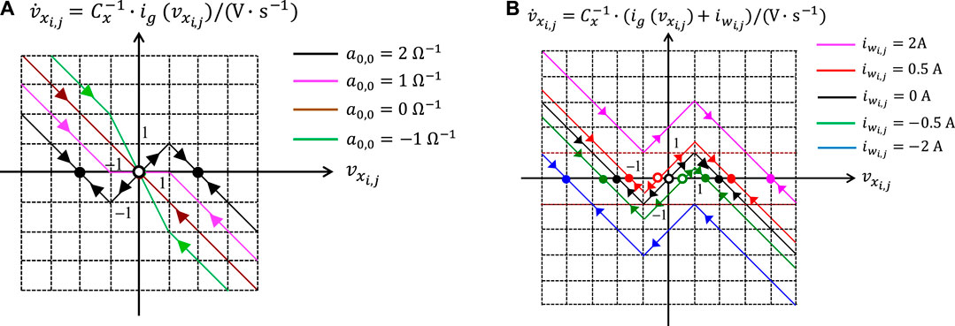
The first aspect to consider for the synthesis of a suitable CNN gene is the choice of a proper value for the self-feedback synaptic weight . As will be clarified through qualitative sketches below, this parameter crucially influences the directed Internal DP Characteristic, consisting of the arrowed locus of the rate of change of the state vs. the state itself under A. As anticipated in section 2.2 in the context of memristors, this type of graphical representation is typically referred to as State Dynamic Route (SDR). In the upper (lower) half of the – plane, where V s−1, arrows, supeimposed over the Internal DP Characteristic, point toward the east (west) to indicate an increase (a decrease) in the state over time. The intersections between this – locus and the horizontal -axis, marked as filled (hollow) circles, denote the stable (unstable) equilibria of the cell state equation under null offset current. All in all, fixing the value for unequivocally determines the dynamical behaviour of the cell state from any initial condition under zero offset current. With reference to9Figure 3, plot (a) shows how affects the shape of the locus of the state rate of change vs. the state itself under . As anticipated in section 2.2 in the context of memristors, a family of directed loci of this kind, one for each value of a control parameter (in this case ), is called DRM, here more specifically referred to as cell DRM. Varying from to , the CNN processing element may exhibit three distinct stability characters:
• If (see the green and brown curves, associated to non-null negative and null self-feedback values, respectively) the cell is monostable with one and only one GAS equilibrium at V.
• If (see the pink curve) each state value within the set V is a stable but not GAS equilibrium for the processing element, which is said to admit a line of equilibria.
• If (see the black curve) the cell is bistable, featuring two locally stable equilibria, one lying at in the negative saturation region, and the other at in the positive saturation region, besides the separatrix between their basins of attractions, namely the unstable equilibrium in the origin.
FIGURE 3
FIGURE 3. (A) Family of Internal DP Characteristics, which a CNN cell admits for each value of the self-feedback synaptic weight in the set . (B) Family of Shifted DP Characteristics, which a CNN cell admits for for each value of the offset current in the set . The set of cell circuit parameter values for the derivation of these viewgraphs is provided here: F, , , and V.
The ordinates of the two breakpoints of the three-segment10 piecewise-linear Internal DP Characteristic, located at , and at , respectively, are of significant importance in the analysis of the Shifted11DP Characteristic (Chua and Roska, 2002), i.e. the locus of the state rate of change vs. the state itself under non-null offset current. First of all, it is important to point out that, under specific hypotheses, including fixed values for all input voltages and thresholds, a standard space-invariant12 CNN is completely stable (Chua and Roska, 2002), in the sense that the state of each cell converges asymptotically toward an equilibrium point , which, in general, depends upon the initial conditon . Moreover, for a completely stable standard space-invariant CNN, according to the bistability criterion (Chua and Roska, 2002), in case the condition
holds true, the slope of the Internal DP Characteristic in the linear region–refer to Eq. 9 – is positive, and, consequently, the stable equilibria of each cell under A are found to lie in either of the two saturation regions of the standard nonlinearity of Eq. 3, as will be elucidated, shortly, through the analysis of the resulting Family of Shifted DP Characteristics, implying that, given the form of the standard nonlinearity Eq. 3, the final value for the output voltage of any processing element is one of the two saturation levels in the set . This is highly desirable for image processing, where, as will be shown through an illustrative example shortly, a CNN equilibria-based computation is typically visualized in the form of a binary output image, coding the final values of the cell output voltages. Importantly, the output voltage of each processing element will attain its final value i.e., one of the two possible saturation levels, already at a finite time instant, let us denote it as , at which its state enters the saturation region, which hosts the equilibrium point . For all the CNN may be considered at steady state as far as its cell output voltages are concerned13. It follows that, irrespective of the location of the CNN cell under analysis, the offset current , which, in general, changes over time during transients, keeps a fixed value for all . This is of significant importance, since from this time instant onward, the Shifted DP Characteristic will no longer bounce, as, on the other hand, may be the case during transients, facilitating the study of the dynamic behaviour of the state from any initial condition .
With reference to the viewgraphs of Figure 3B, neglecting the marginal cases, three are the possible equilibria configurations, which a cell may feature under the bistable criterion hypothesis for A.
• If (see the blue curve) the cell turns into a monostable dynamical system, featuring one and only one globally asymptotically stable (GAS) equilibrium in the negative saturation region at .
• If (see the green, and red curves, associated to negative and positive offset current values, respectively) the processing element keeps its bistable character, featuring an unstable equilibrium in the linear region at , and two-locally stable equilibria, one in the negative saturation region at , and one in the positive saturation region at .
• If (see the magenta curve) the cell turns into yet another monostable dynamical system, admitting one and only one GAS equilibrium in the positive saturation region at .
2.3 A Systematic DRM-Based Methodology to Design Robust CNNs
The standard method (Zarándy, 2003; Itoh and Chua, 2003) to synthesize a suitable CNN gene for the execution of a given computing task is based upon the set up and later solution of an ad-hoc set of inequalities, expressed in terms of unknown gene parameters, ensuring a robust accomplishment of the computing task of interest. The functionalities of a given uncoupled14 standard space-invariant completely stable CNN, satisfying the hypotheses of the bistability criterion, are dictated by a set of local rules, establishing the asymptotic value for the state , and, correspondingly, the steady-state output voltage of each cell , depending upon inputs, and initial conditions of all the processing elements within its neighbourhood.
For the reasons motivated above, in CNN designs for image processing applications, it is common to set the numerical value for the self-feedback synaptic weight so as to guarantee the satisfaction of inequality Eq. 12. Typically, to facilitate the CNN design process, the structure of the gene under synthesis is simplified as much as possible, given the degree of complexity of the computing task, which the cellular array is expected to execute, and/or the values of some of the elements from the 19-number parameter set are assumed to be known. The family of all the possible invariable arrowed Shifted DP Characteristics, which a cell may admit for all for any value, which the offset current may assume, then, under the hypothesis of each of the rules, is then examined, so as to identify the worst-case scenario, where deviations of cell circuit parameters from their nominal values are most likely to induce a change in the cell equilibria configuration15, and, consequently, the emergence of CNN computation errors. The next step is to write down an inequality, establishing a constraint for the offset current, and ensuring that, in such critical scenario, is negative (positive) at the specified initial condition , so that the state would approach a desired equilibrium in the negative (positive) saturation region. Repeating this procedure for each rule allows to derive an inequality set (IS), whose solutions may be determined through numerical techniques, or, in case the number of unknowns is small, via a geometry-based approach. The particular values assigned to the unknowns, allowing to program the CNN with a suitable gene, are then selected to endow the computation with the highest degree of tolerance against parameter variation.
2.4 Edge CNN
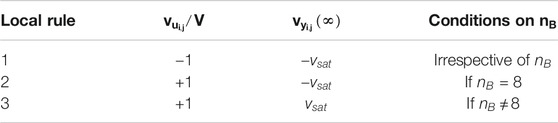
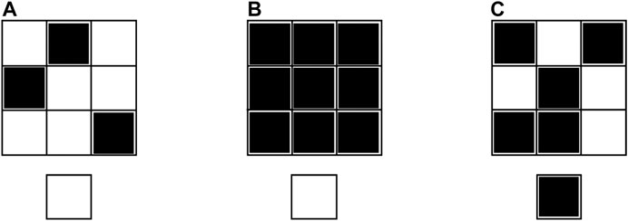
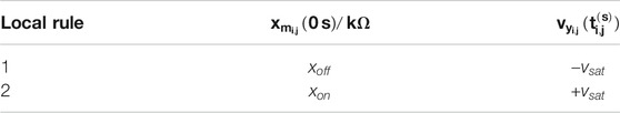
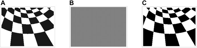
The aim of this section is to synthesize the gene of a standard space-invariant non-autonomous uncoupled CNN so that the resulting nonlinear dynamic array is able to extract the edges from an input binary image. Next, the classical CNN design methodology, briefly described earlier, will be applied to the cell ODE (1) in order to achieve this purpose. The three local rules, which each cell should obey, are reported in Table 1, where defines how many of the 8 adjacent neighbors feature a positive one V-valued input voltage. The first rule establishes that, if the cell features an input voltage equal to , its output voltage at equilibrium is found to attain the negative saturation voltage irrespective of the value of . Plot (a) in Figure 4 depicts a possible pattern around a white pixel at row i and column j in the input binary image under rule 1. Here 3 of the 8 neighboring pixels are black. The pixel in the position of the output binary image is white at equilibrium, as depicted on the bottom of the input pattern. The second (third) rule imposes that, in case the cell features an input voltage equal to , its output voltage at equilibrium is found to attain the negative (positive) saturation voltage in case is exactly equal to 8 (is less or equal to 7). Plot (b) ((c)) in Figure 4 depicts the only (a) possible pattern around a black pixel at row i and column j in the input binary image under rule 2 (3). Here all (4) of the 8 neighboring pixels are black. The pixel in the position of the output binary image is white (black) at equilibrium, as depicted on the bottom of the input pattern.
TABLE 1
TABLE 1. Local rule triplet, which, irrespective of its location within the cellular array, a processing element is requested to obey, for the extraction of edges from an input binary image, preliminarily discretized into a matrix of pixels (, ).
FIGURE 4
FIGURE 4. Graphical illustration of the application of the EDGE CNN local rules 1 for (A), 2 (B), and 3 for (C). Each of the three plots visualizes, on top, a pattern around the pixel located at row i and column j in the input binary image, and, below, the pixel at position in the output binary image at equilibrium.
As clarified by Figure 5A, the CNN under design is expected to extract the edges from an input binary image, visualizing them in the output binary image at steady state. Since the CNN is meant to be uncoupled, the offset current from Eq. 11 reduces to16
FIGURE 5
FIGURE 5. (A) Graphical illustration of the operating principles of the CNN under design. (B) EDGE CNN SDR for zero offset current. Here F, , , and V. The self-feedback synaptic weight (the b value for each of the feedforward synaptic weights, except for ) is set to () ahead of the application of the classical CNN design methodology from Itoh and Chua (2003). The cell equilibria lie at V, at V, and at V.
Assuming that all the feedforward synaptic weights, with the exclusion of , are identical one to the other, namely for all such that , indicating how many, among the 8 neighbours of the cell , feature a negative one V-valued input voltage through the variable , and noting that , the formula Eq. 13 for reduces to
where the argument reveals the dependence of the offset current upon and . Assuming that and are given parameters, the only two unknowns for the specification of a suitable gene are then and z. Figure 5B shows the directed Internal DP Characteristic17. The state Eq. 1 under A admits two locally stable equilibria, located one in the negative saturation region, namely , and one in the positive saturation region, specifically , and separated by an unstable equilibrium, i.e. V, positioned in the linear region.
Let us set the initial condition of the cell ODE (1) to V. Following the line-of-thought inspiring the classical CNN design methodologies, discussed in the seminal papers (Zarándy, 2003) and (Itoh and Chua, 2003), and briefly reviewed above, let us now examine the Family of arrowed Shifted DP Characteristics, which a processing element may admit in all scenarios, which may possibly emerge under the hypothesis of each of the three rules from Table 1.
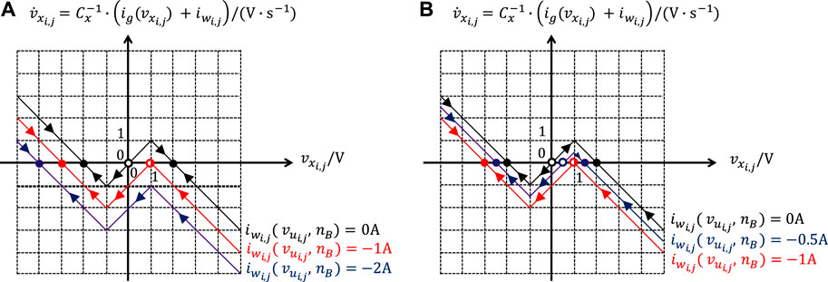
In order to fulfill rule 1, where , a condition should be enforced to ensure that the maximum value, which the offset current may ever attain i.e., , is smaller than the ordinate of the left breakpoint of the – piecewise linear characteristic of Figure 5B. This would guarantee a negative sign for the ordinate of the right breakpoint of the resulting – piecewise-linear characteristic, as is the case for the arrowed blue locus in Figure 6A, illustrating the dynamic route followed by the cell state for , where V, and , under the parameter setting, reported in the caption of Figure 5B. As a result, for all possible values in , the CNN cell would be monostable, and would decrease monotonically over time from the initial condition toward an equilibrium, i.e. , located in the negative saturation region, as established by rule 1. Therefore, the first EDGE CNN design constraint sets an upper bound for the maximum offset current, according to
It is worth pointing out that the farther away from the horizontal axis, within the plane lower half, would be positioned the right breakpoint of the – piecewise-linear characteristic in the worst-case scenario from rule 1, and the more robust would be the EDGE CNN design18.
FIGURE 6
FIGURE 6. Graphs clarifying the line of reasoning behind the DRM synthesis strategy adopted in Itoh and Chua (2003) to select a suitable gene allowing the resulting CNN to apply the local rule triplet of the binary image edge extraction operation in the 9-cell neighborhood of each processing element. The worst-case scenario in rule 1 is analyzed in (A), where and . Setting and , plot (A) allows to investigate rule 2 as well. The worst-case scenario in rule 3 is illustrated in plot (B), where and . The setting of the known parameters of the cell circuit of Figure 2 is reported in the caption of Figure 5B. With reference to plot (A), in the worst-case scenario from rule 1 (in rule 2) the cell state would evolve from the initial condition V toward the equilibrium V, as dictated by the arrowed blue locus, in case were found to be equal to A, while it would keep its initial value V at all times, as governed by the arrowed red locus, if, as a result of the CNN design, the value −1A would be assigned to . In case a cell would feature the blue (red) SDR, either in the worst-case scenario from rule 1 or in rule 2, the CNN would operate (would fail to function) as required. With reference to plot (B), in the worst-case scenario from rule 3, would evolve along the arrowed blue dynamic route from the initial condition toward the equilibrium V provided were found to be equal to −0.5A, while it would keep its initial value V, as established by the arrowed red locus, if, as a result of the CNN design, the value −1A would be assigned to . Theoretically a CNN would properly function if a cell would exhibit the red SDR in the worst-case scenario from rule 3. However, if the cell featured the blue SDR, instead, it would additionally exhibit a little tolerance to deviations of parameters from their nominal values. The directed Internal DP Characteristic, shown in Figure 5B, is depicted once again in black in both plots as a reference. This SDR would induce the cell state to converge toward the equilibrium V. It follows that a cell with such a SDR under V and or under V and (under V and ) would seriously fail to operate as desired (would function properly, exhibiting a good robustness against parameter variability).
Let us now derive the condition allowing the CNN to apply rule 2 from Table 1 in the sphere of influence of any processing cell , which features, as each of its eight neigbours, a positive one V-valued input voltage. Since the expected cell steady-state output voltage is once again , as in rule 1, Figure 6A can be reused to work out a suitable inequality for rule 2 under and . The second EDGE CNN design condition, ensuring that the state of a cell with V and would asymptotically approach an equilibrium, specifically , located in the negative saturation region, is then similar to the inequality Eq. 5, reading as
In order for the CNN under design to apply rule 3 from Table 1 in the neighbourhood of each processing element, which features a positive one V-valued input voltage, and is physically coupled to at least one neighbour with a negative one V-valued input voltage, the minimum value, which the offset current may ever attain, namely should be larger than the ordinate of the left breakpoint of the – piecewise-linear characteristic of Figure 5B. This would ensure a positive sign for the ordinate of the right breakpoint of the resulting vs. piece-wize linear characteristic, as is the case for the arrowed blue locus in Figure 6B, illustrating the dynamic route of the cell state for , where V, and , under the parameter setting, reported in the caption of Figure 5B. Consequently, for all admissible values in , the cell state would monotonically increase over time toward an equilibrium, i.e. , located in the positive saturation region, as required in rule 3. The third EDGE CNN design inequality is then establishing a lower bound for the minimum offset current, i.e.19
For a robust CNN design the right breakpoint of the – piecewise-linear characteristic of a cell in the worst-case scenario from rule 3 should be positioned as farther away as possible from the horizontal axis within the plane upper half20.
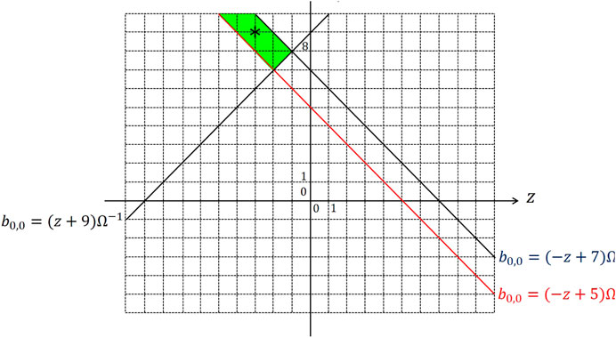
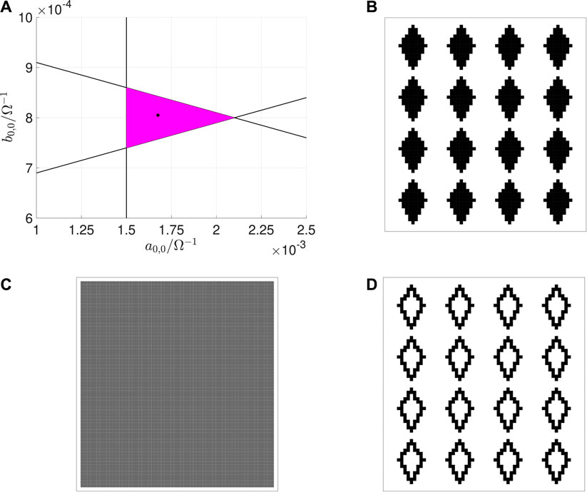
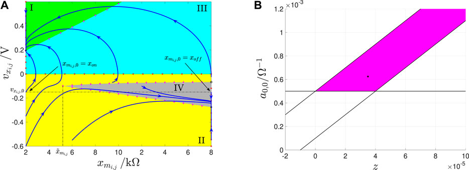
For the parameter setting reported in the caption of Figure 5, the three inequalities Eqs. 15–17 are solved through a geometric approach on the z– parameter plane, as shown in Figure 7, where the green region visualizes the set of admissible solutions. For the specification of a suitable gene, guaranteeing the expected EDGE CNN functionality even in the presence of some small deviation of either of the two parameters z and from their nominal values, it is adviceable to choose a particular solution , whose graphical point-based representation on the parameter plane features an adequate distance from the boundaries of the green region, as indicated by means of an asterisk marker in Figure 7. The gene, synthesized in this section, allows the CNN to extract edges from an input binary image, as displayed in plot (a) of Figure 5.
FIGURE 7
FIGURE 7. Illustration of the geometrical analysis adopted to solve the three inequalities Eqs. 15–17, derived through the classical CNN design method (Itoh and Chua, 2003) to synthesize a suitable gene for a cellular array, intended to extract edges from a given input binary image, and reducing to , , and , respectively, under the parameter setting reported in the caption of Figure 5B. The set of admissible solutions are enclosed within the green area. The asterisk symbol, located at , indicates a reasoned parameter pair choice for the specification of a robust EDGE CNN gene.
2.5 Limitations of the CNN Paradigm and of Its Hardware Implementation
Since each of their processing elements interacts simultaneously with the respective neighbors, CNNs may process multi-variate signals in a massively parallel fashion, as crucially necessary in time-critical application fields, such as industry process control, electronic surveillance, medical augmented reality, and IoT smart sensing. In order to harness more efficiently the bio-inspired operating principles of these nonlinear dynamic arrays, which make them a suitable mathematical framework for modeling neural systems, Chua and Roska proposed an innovative computer, called CNN Universal Machine (CNN-UM) (Roska, 1993), to implement their signal processing paradigm. The CNN-UM, fabricated in various forms over the years through the well-established CMOS technology21 (Vázquez et al., 2018), consists of an array of locally coupled computing units, each of which is endowed with data storage blocks, which allow to distribute the memory across the cellular array, endowing the computing machine with a truly non-von Neumann architecture, and to reconfigure the array so as to solve any computation problem. Thanks to their massively parallel computing power, CNN-UM hardware realizations (Vázquez et al., 2018) may process images at rates as high as 30,000 frames per second. Considering that, furthermore, a universal cellular array may be physically realized within the IC area of a single chip (Vázquez et al., 2018), CNNs are particularly suitable for the development of miniaturized IoT technical systems, in which the integration between a matrix of sensing elements and a network of locally coupled computing units with local stored programmability on board enables information processing at the same location, where data detection takes place. A major problem, which prevents to widen the applicability scope of this class of sensor-processor arrays, is the limited degree of complexity of the dynamical phenomena, which may possibly emerge within their physical media, due to the simplicity of the input-output behaviours of the electrical components employed in the CNN-UM constitutive blocks. Thanks to their extremely rich dynamics, memristors may be adopted in novel designs of cellular computing arrays so as to extend significantly the spectrum of asymptotic spatio-temporal behaviours, which purely CMOS CNNs may currently exhibit. Another critical issue, which affects the performance of technical systems, combining sensing and processing functionalities on the same physical platform, is due to the rather low spatial resolution of state-of-the-art CNN-UM hardware realizations, originating from the presence of spacious data storage units within their computing units, as discussed earlier. This limits the maximum number of sensing and processing elements, which may be paired22 one-to-one within the available IC area of these IoT commercial products (Toshiba Ltd., 2012). The adoption of memristive devices, endowed with memprocessing capabilities, may allow to obviate the inclusion of additional memory banks within the IC design of each CNN-UM computing unit, allowing to shrink considerably its size, and enabling the future realization of sensor-processor arrays with unprecedented spatial resolution, of great appeal to the IoT industry, nowadays. In this respect, it is timely to commence investigations aimed to explore the functionalities of Memristor CNNs (M-CNNs). In general, introducing memristors in the circuit implementation of a CNN processing element23 increases the order of its ODE model, calling for the development of a new theory to investigate the operating principles of the resulting nonlinear dynamic array, and to program its gene to allow the accomplishment of a pre-defined memcomputing task. The theoretical foundations of M-CNNs shall be discussed in the section to follow.
3 Theory of Memristor Cellular Nonlinear Networks
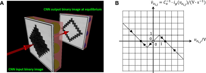
Memristors are the key technology enabler for the hardware implementation of innovative memcomputing paradigms. This section provides some evidence for this claim, establishing the theoretical foundations of a class of cellular memprocessing structures, which we call M-CNNs, as anticipated in section 2.5. In order to realize one of the proposed M-CNNs a first-order non-volatile memristor24 is placed in parallel with the capacitor in the circuit implementation of each cell of the two-dimensional standard time- and space-invariant CNN (Chua, 1998), which was discussed in section 2.1. The memristive cell of the novel nonlinear dynamic array is shown in Figure 8.
FIGURE 8
FIGURE 8. Circuit implementation of the M-CNN cell (, ). In this study the cell circuit parameters are assumed to be invariant across the bio-inspired memristive array. As a result, the following assumptions are made: , , , and . Two are the main contributions to the capacitor current : one, given by the addition between , , and , is a function of the two cell states, while the other, expressed by the sum of the memcomputing core currents, which flow through the 18 branches appearing to the right of the memristor, except for the self-feedback synaptic current, capture mostly the impact of input and output voltages of the 8 neighbors on the dynamics of the cell states themselves.
The next section reports the mathematical description of the proposed memristive cellular array.
3.1 M-CNN Model
The M-CNN cell of Figure 8 may be described by the following pair of first-order coupled ODEs25 (, ):
The first ODE Eq. 18 governs the time evolution of the state of the first-order nonvolatile resistance switching memory , which the M-CNN cell acccommodates, according to an enhanced variant of a voltage-controlled memristor model, originally formulated by Pershin and Di Ventra (Pershin et al., 2009), and capable to capture the switching kinetics of real memristor devices (Jo et al., 2009), as discussed in Pershin and Di Ventra (2011). The model of the resistance switching memory in the cell is a first-order element from the class of generic memristors, defined by the DAE set
Note that, within the processing element , the memristor voltage coincides with the capacitor voltage , thus the expression for the memristor current in Eq. 21 reduces to
The state evolution function and the memductance function in the Pershin and Di Ventra model of the memristor in the M-CNN cell are respectively expressed by
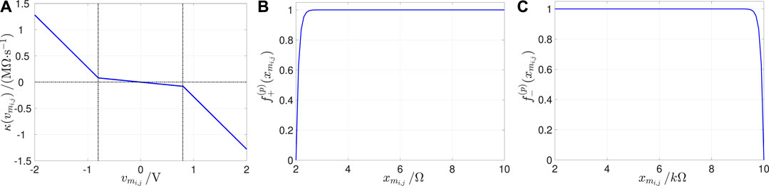
The memristor state , representing the device memristance, is constrained to lie at all times within the closed set , where and denote the lowest and highest possible device resistances, respectively. With reference to Eq. 23, stands for the Heaviside function, while is a piecewise-linear nonlinearity of the form
where and are coefficients, measured in units , denoting the smaller and larger slopes of the characteristic for and , respectively, where represents the memristor switching threshold voltage. Figure 9A depicts the – chapacteristic for the parameter setting reported in its caption.
FIGURE 9
FIGURE 9. (A) Course of as a function of for V−1 s−1, V−1 s−1, and V. (B,C) Window functions, appearing in the state evolution function Eq. 23, and preventing from decreasing below (increasing above) the lower (upper) bound () under positive (negative) memristor voltages. Here , , and .
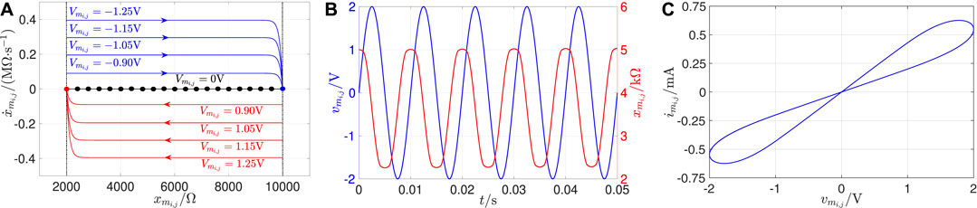
Since the memristor state existence domain is finite, the state evolution function in Eq. 23 is endowed with boundary conditions, which ensure that never decreases below (increases above) its lowest (largest) possible value under . In order to facilitate the numerical simulation of the memristor DAE set, we reformulate the boundary conditions as compared to their original definition26 in the Pershin and Di Ventra model (Pershin et al., 2009), adopting continuous and differentiable functions, inspired to Biolek’s window (Biolek et al., 2009), and reading as
where controls the decay rate of the window function Eqs. 26, 27 as approaches (). As graphically illustrated in plot (b) ((c)) of Figure 9 for the parameter configuration provided in its caption, the window function in Eqs. 26, 27 enforces the memory state evolution function Eq. 23 to feature a zero, and, consequently, the memristor ODE Eq. 18 to admit an equilibrium at under positive (negative) values of the capacitor voltage. Since the memory state ODE Eq. 18, with evolution function expressed by Eq. 23, is of first-order, the classical DRM graphical tool (Chua, 2018a) may be applied to investigate the memristor nonlinear dynamics. The DRM of the modified Pershin and Di Ventra memristor model is illustrated in Figure 10A for the parameter arrangement defined in its caption. The DC value , assigned to the voltage falling across the resistance switching memory, parametrizes the family of memristor SDRs. Within the family of vs. loci, the characteristic obtained for V, known as POP, provides hints on the nonvolatile memory capability of the circuit element. On the basis of the memristor model under focus, the POP is a segment of the axis lying between and . Each of the points on this segment–shown in black in Figure 10A–represents a stable but not asymptotically stable equilibrium (Strogatz, 2000) for the ODE Eq. 18 with state evolution function Eq. 23. Particularly, the existence of a continuum of equilibria, namely , for the memristor state equation under zero input clearly reveals that the resistance switching device is an analogue non-volatile memory. Any value for within its existence domain is a possible state, which the memristor may store, from the time at which the power is turned off, till the time at which a new voltage stimulus is applied between its terminals. With regard to the – loci, associated to nonzero values for , in Figure 10A, the device asymptotically approaches the fully off (fully on) resistive equilibrium state in case any negative (positive) DC voltage is applied continually between its terminals, as indicated by the arrow superimposed on each blue (red) characteristic, which dictates a memory state rate of change increasing monotonically with . Irrespective of the negative (positive) DC value assigned to the memristor voltage, the upper (lower) bound in the memristor state existence domain is found to be a globally asymptotically stable equilibrium for the ODE (18) with state evolution function Eq. 23. For the very same parameter setting, Figure 10B demonstrates now the smooth periodic change, which the state of the memristor in the cell undergoes over each cycle of a sinusoidal voltage appearing between its terminals, and mathematically expressed by , where V and Hz. Clearly, at any given time instant, the cell is effectively a second-order dynamical system with degrees of freedom provided one by the memristor state and one by the capacitor voltage, which is also illustrated in plot (b) of Figure 10. Visualizing the memristor current flowing through the memristor as a result of the capacitor voltage from plot (b) vs. the capacitor voltage itself, the resulting pinched hysteresis loop, shown in Figure 10C, gives further evidence for the analogue dynamic behaviour of the cell memristor. The second M-CNN cell ODE Eq. 19 governs the time evolution of the cell capacitor voltage within the memcomputing core of the circuit of Figure 8. Its right hand side is identical as in the ODE Eq. 1 dictating the rate of change of the capacitor voltage within the computing core of the cell of the standard time- and space-invariant two-dimensional CNN discussed in section 2.1, except for the presence of an additional addend, resulting from the current through the memristor. It follows that the expression for the offset current of the memristive processing element of Figure 8 is still given by Eq. 11, while, using Eq. 22 to express the current through the memristor, the formula for the cell Internal DP Component features the new form
in which Eqs. 22, 24 were employed to model the cell memristor current and the memductance function , respectively. It is worth to note that the number of variables in the argument of is a signature for the order of the cell, as can be inferred by comparings Eqs. 8–10 and Eqs. 28–30. The classical cell DRM technique (Chua, 2018a), reviewed in section 2.2, and adopted for the analysis and synthesis of standard CNNs with first-order processing elements, is applicable to dynamical systems with one degree of freedom only. As a result, the development of a systematic procedure to investigate and design M-CNNs with second-order memristive processing elements calls for a preliminary generalization of the DRM graphic tool. Drawing inspiration from the phase portrait concept from the theory of nonlinear dynamics (Strogatz, 2000), the next section introduces a new system-theoretic notion, which we name Second-Order DRM (DRM2), enabling the investigation of the memcomputing capabilities of cellular nonlinear arrays with second-order memristive cells.
FIGURE 10
FIGURE 10. (A) SDRs foliating from the memristor DRM for V. The blue (red) arrowed loci are associated to negative (positive) values for the memristor voltage. In the first (latter) case, the larger is , and the higher is the speed of the memristor state in its motion toward the equilibrium . The black locus represents the memristor POP. (B) Proof of evidence for the analogue dynamic response of the memristor state, hosted by the cell , to a sinusoidal voltage of the form , with amplitude V and frequency Hz, appearing between its terminals. (C) Pinched hysteresis loop emerging on the – plane as a result of the device periodic excitation illustrated in (B). The memristor model parameters are set as follows: V−1 s−1, V−1 s−1, V, , , .
3.2 A Generalized DRM Technique for the Analysis of M-CNNs With Second-Order Processing Elements
In this section we extend the classical DRM methodology (Chua, 2018a) for the analysis of a nonlinear dynamic system with two degrees of freedom. Focusing, in particular, on the second-order M-CNN cell under study, the – phase plane is the most natural domain, where the dynamical evolution of the two states of the system, described by Eqs. 18, 19, may be studied. Let us first introduce the concept of State Dynamic Portrait (SDP).
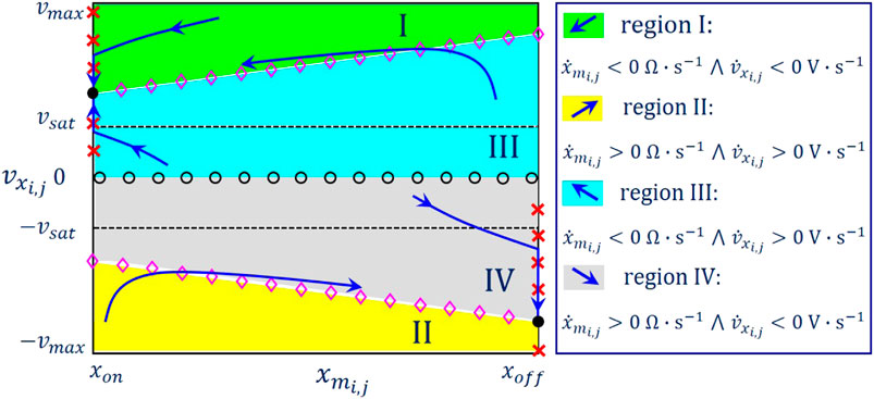
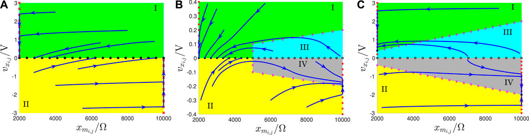
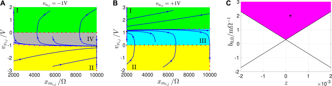
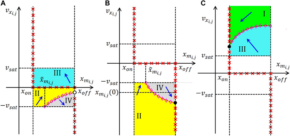
Remark 2. With reference to the qualitative drawing in Figure 11, a SDP is a two-dimensional graph associated to a prescribed choice for the offset current value. It may be obtained as follows. First, the phase plane – is partitioned into at most 4 distinct regions, differing in the and/or in the , and distinguished according to the following coding map:
• Green region I: V/s and .
• Yellow region II: V/s and .
• Cyan region III: V/s and
• Gray region IV: V/s and
Then the loci /s and /s – respectively known as and nullclines (Strogatz, 2000) – as well as their intersections – i.e., the equilibria of the ODE set Eqs. 18, 19 – are marked on the phase plane using the following symbolism:
• Red crosses: /s.
• Magenta diamonds: /s.
• Black circles: /s and /s.
Particularly, the local instability (stability) of an equilibrium, studied by linearizing the state equations and studying the properties of the Jacobian, is graphically illustrated in a given SDP by means of a hollow (filled) black circle. The dynamical behaviour of the state variables from any initial condition of interest may be qualitatively inferred by inspecting the direction of the vector field . In fact, phase plane trajectories27, moving through regions I, II, III, and IV, proceed in the south-west, north-east, north-west, and south-east directions, as time goes by, respectively. The numerical integration of the pair of first-order coupled ODEs Eqs. 18, 19, for initial conditions in the set of interest, allows to confirm this qualitative investigation on a quantitative basis, allowing to endow the partitioned plane, already accomodating nullclines and equilibria, with a number of phase plane trajectories, extracted by plotting the two solutions and of the model equations one against the other, and indicating, through the guide of arrows, placed on top of them, how the second-order M-CNN cell state evolves with time from prescribed starting points. An arrowed phase plane trajectory, marked in blue on a given SDP, is called a Second-Order SDR (SDR2). Finally, the family of SDPs, obtained for each offset current value within a certain set of interest, takes the name of Second-Order DRM (DRM2). The proposed generalized DRM methodology may be used to analyze the operating principles of a given M-CNN with second-order memristive cells. Most importantly, the DRM2 graphical tool allows to develop a systematic procedure to program one of the memristive cellular arrays under focus for the execution of a predefined memcomputing task, as outlined in the next section.
FIGURE 11
FIGURE 11. Exemplifying SDP, which the M-CNN cell would typically feature under A, if . The capacitor voltage range under display is , with . The linear region is the rectangular domain enclosed within the two black dashed horizontal lines. The direction of motion of the state vector in regions I, II, III, and IV is graphically illustrated in the legend.
Remark 3. The DRM2 graphic tool features a much more general applicability scope than this paper demonstrates. In fact, it allows to investigate any second-order dynamical system, including memristive circuit elements with two degrees of freedom.
3.3 A Rigorous DRM2-Based Methodology for Robust M-CNN Design
The proposed DRM2-based M-CNN design methodology (Ascoli et al., 2020a) allows to program the memristive nonlinear dynamic array i.e., to choose numerical values for the 19 cell core parameters28 (), in such a way that the processing element may implement a predefined set of rules29 (Chua, 1998), which, depending upon the specific data storage or processing operation to be executed, dictate the steady-state value30 of its output voltage for any combination of input voltage and initial conditions and of its two dynamical states, and under specific conditions involving neighboring or remote processing elements. The proposed M-CNN design methodology complementing similar works – discussed in section 2.3 – on the synthesis of CNN genes (Zarándy, 2003; Itoh and Chua, 2003), is based upon the following steps:
1. On the basis of the memcomputing task assigned to a given M-CNN, and with reference to the processing element , the designer should first roughly identify, under any possible combination of input voltage , and of initial capacitor voltage and memory resistance , and for any condition involving neighboring and/or remote cells, envisaged by the rule set, the most suitable partition of the two-dimensional state space –, which would guide the respective phase-plane trajectory toward an appropriate equilibrium. In other words, this step allows to specify the Family of SDPs i.e., the cell DRM2, under target.
2. In order to derive numerical values for the parameter set , where , so as to endow the cell with the specified DRM2, a number of inequalities, constraining, for each scenario of any rule, the behaviour of the and of the across the phase plane – so as to control the number and stability properties of the equilibria, which it accommodates, are written down31 through the use of the second-order ODE system Eqs. 18, 19, with the expression for the offset current , appearing in the latter state equation, preliminarily simplified as much as possible as compared to its general formula from Eq. 11, so as to implement the given data storage or processing task as efficiently as feasible.
3. A set of cell parameter values, satisfying concurrently all the aforementioned inequalities, shall be determined by means of a graphical approach, or through a numerical algorithm, depending upon the number of unknowns. Integrating numerically the state Eqs. 18, 19 of the M-CNN cell for prescribed input voltage and vector state initial condition in each scenario encompassed in any rule, the resulting phase plane trajectories on the relevant SDP shall be found to evolve progressively toward the desired equilibria, allowing the cellular array to accomplish a predefined memcomputing task.
3.4 Application of the M-CNN Design Methodology to Execute Fundamental Memcomputing Tasks
In this section the proposed cell DRM2 synthesis technique is applied to the cell model Eqs. 18, 19 to program the M-CNN to execute an image processing operation and a couple of memory functions, namely the data storage and retrieval tasks. Before presenting the M-CNN design examples, it is instructive to identify the most important properties of the second-order system Eqs. 18, 19 through the application of fundamental concepts from the theory of nonlinear dynamics (Strogatz, 2000).
From the first M-CNN cell ODE Eq. 18, the formulas for the nullclines (Strogatz, 2000) are
Employing now the second M-CNN cell ODE Eq. 19, the nullclines are found to be expressed by
for , by
for , and by
for
Remark 4. As it follows from Eq. 29, under A, the nullclines in the linear region consist of the segment, lying along the axis, and comprised between and , and, in case (see Figure 12B for an example, where ), where
also of the two disjoint sets , and for .
FIGURE 12
FIGURE 12. Cell SDP, emerging for the fixed circuit parameter setting from Table 1, under A, and , and featuring a continuum of stable equilibria for (A), a stable isolated equilibrium, as well as a line of equilibria with stable (unstable) character to the left (right) of a bifurcation point for (B), and, finally, two stable isolated equilibria, as well as a continuum of unstable equilibria for (C).
Remark 5. The application of the proposed design method to the specific M-CNN cell model Eqs. 18, 19 is unable to control existence and/or massage the shape of the nullclines, which are invariably set by equations Eqs. 31–33. However, the number and graphical look of the versus loci from equations Eqs. 34–36 may be altered by tuning the cell model parameters, they are function of, so as to allow the synthesis of a suitable cell DRM2 for the accomplishment of a predefined memcomputing task. The equilibria, lying at the intersections between the and nullclines, are located at
if
in the negative saturation region, at
if
as well as at
if
in the linear region, and at
if
in the positive saturation region.
Remark 6. Under A, each point defined as
represents a possible equilibrium for the M-CNN cell in the linear region. Moreover, in case (), with () defined in equation Eqs. 37, 38, also each point along the vertical line of the – phase plane, passing through the memristor state upper (lower) bound (), and stretching over the capacitor voltage range () denotes an additional M-CNN cell equilibrium in the linear region (Ascoli et al., 2020b). From the first M-CNN cell ODE Eq. 18, it follows that the memristor state increases if
and decreases if
Thus, as revealed by the illustrative cell SDP example of Figure 11, the motion of a trajectory point on a given SDP points toward the east (west) in the phase plane lower (upper) half. Inspecting now the second M-CNN cell ODE (19), the capacitor voltage is found to increase provided
for , provided
for , and provided
for , and it decreases provided the inequality sign in each of the -dependent conditions Eqs. 50–52 is inverted. On the basis of inequalities Eqs. 50, 52, dictating the conditions under which in the negative, linear, and saturation region, respectively, it is now possible to understand the reason why the trajectory point moves northward or southward in the illustrative cell SDP example of Figure 11.
3.4.1 Zero Offset Current Scenario
It may be proved that, unlike a standard CNN processing element, the M-CNN cell may never exhibit monostability for A. In other words, under no circumstances may the respective SDP host one and only one globally asymptotically stable equilibrium (Strogatz, 2000). Table 2 sums up (Ascoli et al., 2020b) the location and local stability property of each equilibrium, which the M-CNN cell may admit under zero offset current depending upon the self-feedback synaptic weight .
TABLE 2
TABLE 2. Location and local stability property of each of the equilibrium points, which a M-CNN cell may possibly admit, depending upon , under A (Ascoli et al., 2020b). The coordinates of , , and are indicated in Eqs. 39, 47, and 45, respectively. With reference to the table content, we define , and . The marginal case (), in which, as mentioned in Remark 6, an additional line of equilibria, namely each point along the vertical line passing through the memristor state upper (lower) bound and stretching across the capacitor voltage range (), appears in the linear region, is not tabulated here, but the interested reader is invited to consult (Ascoli et al., 2020b).
Specifying the values32, reported in Table 3, for all the fixed parameters of the cell circuit of Figure 8, the viewgraphs in plots (a), (b), and (c) of Figure 12 illustrate the SDP of a M-CNN processing element, accommodating no linear resistor in the memcomputing core, under zero offset current, and for a specific value of the self-feedback synaptic weight in the first, second, and third of the three sets reported in Table 2 and Ascoli et al. (2020b).
TABLE 3
TABLE 3. Setting of specific M-CNN cell circuit parameters, specifically α, β, and from Eq. 25, , , and p from Eqs. 26, 27, from Eq. 19, I from Eq. 4, from Eq. 2, as well as and from Eq. 3, which are kept unchanged in the design examples to follow.
3.4.2 Non-Zero Offset Current Scenario
Allowing a non-null offset current, accounting mostly for the coupling effects, to flow through the capacitor in the circuit of Figure 8 may endow the processing element with monostability, which is useful for the accomplishment of certain mem-computing tasks, as will be clear from the discussion of some M-CNN designs in the sections to follow. Table 4, in which and are defined as
classifies the number, location, and local stability property of all the equilibria which a M-CNN cell may possibly admit for all the possible combinations of self-feedback synaptic weight and offset current .
TABLE 4
TABLE 4. Location and local stability property of each of the equilibrium points, which a M-CNN cell may possibly admit, depending upon and . The coordinates of equilibria , , , and are respectively specified in Eqs. 39, 41, 43, and 45. The formulas for , , , and are respectively expressed by Eqs. 37, 38, 53, and 54. The local stability nature of each of the possible cell equilibria is also revealed. The analysis of the marginal cases is omitted from this table.
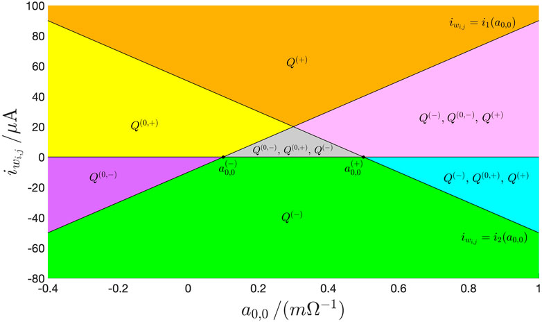
Remark 7. Interestingly, this table allows to draw the codimension-2 bifurcation diagram of Figure 13, in which, without loss of generality, was set to. This graph, which, taking inspiration from CNN theory (Chua, 1998; Chua and Roska, 2002) is called M-CNN Primary Mosaic, visualizes the partitioning of the – plane in domains differing one from the other in at least one of the stable equilibria, which the solutions of the ODE of a cell from the class of uncoupled M-CNNs may possibly approach depending upon the initial conditions. For each of such domains in Figure 13, a distinct color is chosen to fill the space within its boundaries, and the indication of the stable and unstable equilibria, which the M-CNN cell admits for any pair residing therein, is given.In this manuscript the proposed DRM2-based M-CNN design methodology shall be applied to the model Eqs. 18, 19 of a cell belonging to the class of uncoupled M-CNNs, and featuring an offset current, which, in comparison to its most general formula, namely Eq. 11, reduces to Eq. 13.
FIGURE 13
FIGURE 13. The M-CNN Primary Mosaic: codimension-2 bifurcation diagram illustrating all the admissible equilibria the two states of the second-order cell from the class of uncoupled M-CNNs may approach asymptotically depending upon the specific region of the – parameter plane, in which the values assigned to the self-feedback synaptic weight and to the offset current reside. A red (black) color is adopted for the symbol of each unstable (stable) M-CNN cell equilibrium, as specified in Table 2. Without loss of generality, here was set to . The coordinates of , , , and are indicated in Eqs. 39, 41, 43, and 45. The formulas for , , , and are respectively expressed by Eqs. 37, 38, 53, and 54. Details on the possible steady-state behaviours of the M-CNN cell in the marginal cases A, , and have not been reported in the bifurcation diagram to keep the illustration as clear as possible. Importantly, as studied earlier, under zero offset current, irrespective of the value specified for , in the linear region the cell admits each equilibrium , which, according to Eq. 47, lies along the segment of the horizontal axis of the – phase plane comprised between and .
4 M-CNN as a Bio-Inspired Image Processing Engine
A M-CNN may be programmed to carry out any image processing operation, which a classical CNN is able to execute. To provide some evidence for this claim, the next section discusses the system-theoretic design of a memristive cellular array for the extraction of edges from a binary image.
4.1 Edge M-CNN
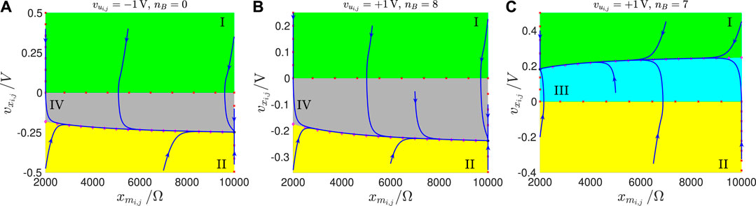
This section is devoted to the design of a memristive array capable to extract the edges from an input binary image featuring as many rows and columns as the M-CNN. The local rule triplet, each M-CNN cell, featuring the circuitry shown in Figure 8, is requested to comply with, so as to execute this image processing task33, are reported in Table 1 from section 2.4. In order to ensure that the memprocessing elements obey this local rule set, it is wise to synthesize the cell SDP pertaining to each scenario from rules 1 and 2 (rule 3) in such a way that it accommodates one and only one equilibrium located in the negative (positive) saturation region i.e., (), as specified by Eqs. 39, 45. In order to ease the understanding of the steps of the proposed M-CNN design methodology, it is adviceable to provide its result in advance. Plots (a), (b), and (c) of Figure 14 respectively illustrate the SDP of a M-CNN processing element, which obeys34 rule 1 for , rule 2, and rule 3 for . As may be inferred by inspecting plots (a) and (b) (plot (c)), here the cell monostability in both rules 1 and 2 (in rule 3) is enforced by making sure that only the negative (positive) saturation region hosts a nullcline, as expressed by Eqs. 34, 36, and highlighted by means of magenta diamonds, and imposing that such characteristic form a point of intersection, as defined by Eqs. 39, 45, and marked via a black circle, with the vertical nullcline Eqs. 31, 33 indicated through red crosses in the phase plane lower (upper) half. Adopting such a cell DRM2 synthesis strategy, in any scenario of rule 1 and for rule 2 (under all circumstances in rule 3), a state vector positioned below/above the nullcline Eqs. 34, 36 is constrained to move in the north/south direction, bending eastward or westward in the phase plane lower or upper half, respectively, toward the point Eqs. 39, 45, denoting, as a result, a globally asymptotically stable equilibrium for the second-order ODE system Eqs. 18, 19, as the filling of the respective black circle marker in plots (a) and (b) (plot (c)) of Figure 14 clearly indicates. Plots (a.1) (a.2), and (a.3) ((b.1), (b.2), and (b.3)) of Figure 15 graphically visualize the steps, envisaged by the proposed cell SDP synthesis approach, and discussed shortly, to shape the phase portrait of the second-order ODE Eqs. 18, 19 in the linear, negative (positive) saturation, and positive (negative) saturation regions, respectively, so as to enforce local rules 1 and 2 (rule 3) from Table 1. Through a rigorous mathematical analysis of Eqs. 18, 19 in each region of the standard output nonlinearity Eq. 3 we shall next derive an ad-hoc IS set, allowing to massage the cell DRM2, as illustrated in Figure 15. Previous to initiate this investigation, a couple of aspects should be pinpointed. Firstly, the cell ODE initial condition may be chosen arbitrarily, since, as mentioned earlier, irrespective of the rule, the phase plane will be allowed to host one and only one GAS equilibrium in any possible scenario. Secondly, we assume the same expression for the offset current as in the EDGE CNN design, namely Eq. 14. Let us suppose that the parameter values for and are known. As a result, the M-CNN gene synthesis technique will target the derivation of suitable values for and . An appropriate IS in these two unknowns is derived next. The analysis of Eqs. 18, 19 focuses first on the linear region of the phase plane.
FIGURE 14
FIGURE 14. (A) SDP of a cell featuring the input voltage in the worst-case scenario of rule 1. (B,C) SDP of a cell featuring the input voltage in the only scenario of rule 2 (in the worst-case scenario of rule 3).
FIGURE 15
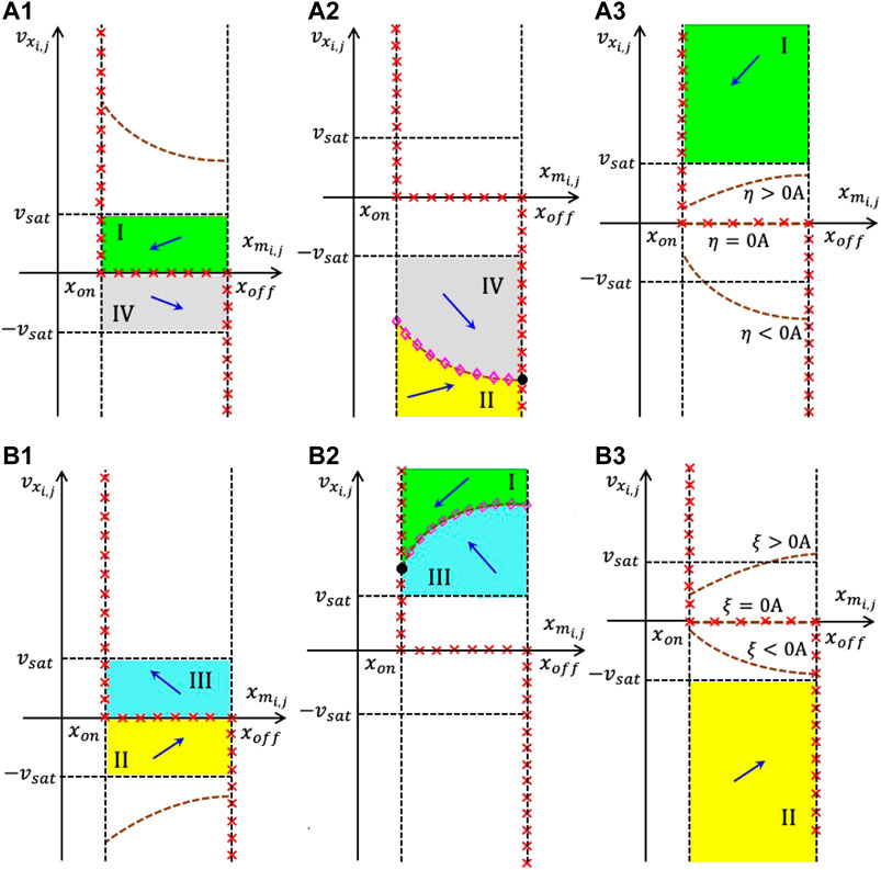
FIGURE 15. Qualitative visualization of the strategy adopted to massage the shape of the cell DRM2 in the EDGE as well as in the STORE M-CNN designs. Here the stepwise application of the proposed systematic gene synthesis methodology in the linear region (a.1) ((b.1)), in the negative (positive) saturation region (a.2) ((b.2)), and in the positive (negative) saturation region (a.3) ((b.3)) of the phase plane – enables to enforce the appearance of a single nullcline, namely Eqs. 34, 36, and the existence of one and only one equilibrium, specifically Eqs. 39, 45, in the EDGE cell SDP, which emerges in each scenario of rule 1 and for rule 2 (under all circumstances in rule 3) from Table 4, as well as in the STORE cell SDP, which forms under the hypothesis of rule 1 (2) from Table 5. With reference to the first (latter) set of scenarios, combining plots (a.1), (a.2), and (a.3) ((b.1), (b.2), and (b.3)) provides an ad-hoc cell SDP, given that the phase-plane partition guides all trajectories toward the unique equilibrium in the negative (positive) saturation region, as desired in the EDGE as well as in the STORE M-CNN designs. The dashed brown curve without magenta diamonds in (a.1) ((b.1)) is the characteristic, expressed by Eq. 35, and constrained to lie in the region , so as to keep the linear region free of nullclines. The dashed brown curve with magenta diamonds in (a.2) ((b.2)) represents the only locus of points of the phase plane, where , as expressed by Eqs. 34, 36. Finally, the set of three dashed brown curves without magenta diamonds in (a.3) (b.3) constitute the possible courses of the characteristic, expressed by Eqs. 34, 36, constrained to lie in the region , so as to keep the positive (negative) region free of V s−1 loci, depending upon the sign of (). Interestingly, the function of Eqs. 34, 36 is either concave down and monotone increasing if () or coinciding with the horizontal axis if (), or even concave up and monotone decreasing if ().
4.1.1 Edge M-CNN Cell DRM2 Synthesis in the Linear Region
With reference to plot (a.1) (b.1) of Figure 15, the aim of this section is to make sure that, under all circumstances in rule 1 and for rule 2 (in all scenarios of rule 3), the characteristic of Eq. 35 lies entirely within the domain , as indicated by means of a dashed brown curve without magenta diamonds. The inequality
ensures a positive sign for the denominator of the rational function on the right hand side of Eq. 35 irrespective of the value assumed by the memristor state throughout its existence domain . Provided the constraint Eq. 55 holds true, enforcing a negative (positive) polarity for the offset current35 in each scenario of rule 1 and for rule 2 (under all circumstances in rule 3) via
ensures that the – locus, expressed by Eq. 35, falls entirely within the phase plane positive (negative) half in these cases. It is simple to show that, under the satisfaction of constraint Eq. 56 with the first (second) inequality sign in rules 1 and 2 (rule 3), the function features an upward (downward) concavity, decreasing (increasing) monotonically with the memristor state, as shown in plot (a.1) ((b.1)) of Figure 15. As a result, under all possible circumstances in rule 1 and for rule 2 (in all scenarios of rule 3) the characteristic lies completely within the positive (negative) saturation region, as depicted in Figure 15 (a.1) ((b.1)), provided
Let us now study the direction of motion of the state vector throughout the linear region. The enforcement of inequality Eq. 55 endows the second factor on the left hand side of constraint Eq. 51 with a strictly positive sign. It follows that, within the domain , the capacitor voltage of the cell circuit of Figure 8 increases over time if
Since, as established by constraint Eq. 57, in rules 1 and 2 (rule 3) the right hand side of inequality Eq. 58 assumes values larger (lower) than throughout the memristor state existence domain, phase plane trajectories of the linear region move toward the south (north), bending eastward or westward in the phase plane lower or upper half, as established by condition Eq. 48 or Eq. 49, visiting36 the gray (yellow) region IV (II) or the green (cyan) region I (III), respectively, as indicated in plot (a.1) ((b.1)) of Figure 15.
4.1.2 Edge M-CNN Cell DRM2 Synthesis in the Saturation Regions
The goal of this section is twofold. On one hand, in each scenario of rule 1 and for rule 2 (under all circumstances from rule 3) the cell SDP is expected to accommodate one and only one GAS equilibrium point, specifically Eqs. 39, 45, over the domain , as indicated by the black-filled circle in plot (a.2) (b.2) of Figure 15. On the other hand, in order to avoid the existence of a locus in the positive (negative) saturation region under any circumstance in rule 1 and for rule 2 (in all scenarios of rule 3), the whole characteristic, expressed by Eqs. 34, 36 should fall below (above) the horizontal line , as sketched in Figure 15 (a.3) ((b.3)), where the three dashed brown curves show its three possible shape variants. It is straightforward to verify that, in view of inequality Eq. 56, in any of the possible scenarios of rule 1 and for rule 2 (under all circumstances in rule 3), the nullcline Eqs. 34, 36 features upward (downward) concavity as it decreases (increases) monotonically with the memristor state. As a result, imposing that it further assumes a value smaller (larger) than the negative (positive) saturation voltage, when the memristor state sits at its lowest bound i.e.,
in each of the first (latter) set of scenarios, ensures that this unique V s−1 locus lies within the negative (positive) saturation region for all , as visualized through a dashed brown curve with magenta diamonds in plot (a.2) ((b.2)) of Figure 15. This in turn allows the formation of a cell equilibrium, as expressed by Eqs. 39, 45, and visualized through a black circle in plot (a.2) ((b.2)) of Figure 15, for each value of under , and for under (for each value of under ). Thus, with regard to rules 1 and 2 (rule 3), recalling that features a positive sign throughout the phase plane lower half, as established by Eq. 48, and recalling the condition Eqs. 50, 52, which guarantees an increase of the cell capacitor voltage over time in the negative (positive) saturation region, phase plane trajectories, visiting the domain , bend toward the east (west), evolving over time in the north or south direction from initial conditions lying below or above the nullcline Eqs. 34, 36, respectively, going through the yellow (cyan) region II (III) or gray (green) region IV (I), as clearly indicated in Figure 15 (a.2) ((b.2)). Manipulating the constraint, obtained by choosing the first (second) inequality sign in Eq. 57, it is simple to demonstrate that, depending upon its polarity, namely the sign of (), the – locus Eqs. 34, 36 may exhibit one of three possible graphs, as depicted in plot (a.3) ((b.3)) of Figure 15, lying, nevertheless, entirely below (above) the horizontal line , under all circumstances from rule 1 and in rule 2 (for each scenario of rule 3). Given that, with reference to the positive (negative) saturation region, the memristor state experiences a strictly monotonic decrease (increase) over time according to constraint Eqs. 48, 49, while provided condition Eqs. 50, 52 is satisfied, phase plane trajectories, visiting the domain in the SDP of any cell obeying rules 1 and 2 (rule 3), are expected to evolve in the south-west (north-east) direction, passing through the green (yellow) region I (II), as visualized in plot (a.3) ((b.3)) of Figure 15. Looking at the direction of motion of phase-plane trajectories across the phase plane (refer to plots (a.1)-(a.3) ((b.1)-(b.3)) of Figure 15), it is evident that the unique equilibrium Eqs. 39, 45, which the cell admits under the hypotheses of rules 1 and 2 (rule 3), is GAS, as indicated through the filling of its black circle marker in Figure 15 (a.2) ((b.2)). In regard to rule 1 (3), taking into account the negative sign assumed for the common value b of the off-center synaptic weigths in the feedforward template, it may be easily realized that, under , the loci (34), (35), and (36) are closest to the horizontal lines (refer to plot (a.2) ((b.3))), (refer to plot (a.1) ((b.1))), and (refer to plot (a.3) ((b.2))), respectively. It follows that, with regard to rule 1 (3), the constraint triplet, obtained from Eqs. 56, 57, and 59 by choosing the first (second) inequality sign, should be evaluated only in the worst-case scenario, in which none (seven) of the eight neighbours of the M-CNN cell features (feature) a positive one V-valued input voltage. Combining the resulting six conditions with the rule 2-based constraint triplet Eqs. 56, 57, and 59 under the first inequality sign option, and with Eq. 55, provides a total number of 10 inequalities in the unknowns and . Fixing the values for two cell core circuit parameters, namely z, and b, respectively set to and to , and assigning the value to the conductance of the linear resistor37 in parallel to the capacitor in the memcomputing core of Figure 8, the two conditions, respectively descending from constraint Eqs. 56, 57 under the first inequality sign option for the worst-case scenario from rule 1, and under the second inequality sign option for the worst-case scenario from rule 3, are found to be identical one to the other, allowing to discard a couple of inequalities from the 10 aforementioned constraints. Manipulating the remaining 8 inequalities, it may be shown that only 3 of them are non-redundant, specifically constraint Eq. 55, and the pair of conditions, which respectively originate from the variant of Eq. 57, which is associated to the choice of the first inequality sign in the worst-case scenario from rule 1 and in the only scenario from rule 2. These 3 inequalities may be solved numerically, but, given their low number, a geometric approach is adopted here to derive suitable values for the self-feedforward and self-feedback synaptic weights. The magenta region in the – parameter plane of Figure 16 depicts the domain of admissible solutions of the non-redundant inequality triplet. Choosing the particular solution, which is indicated through an asterisk symbol, namely , plots (a), (b), and (c) of Figure 14 illustrate the SDPs, which foliate from the cell DRM2 in the worst-case scenario from rule 1, where mA, in the sole scenario admissible in rule 2, where mA, and in the worst-case scenario from rule 3, where mA, respectively. Inspecting the cell SDP from plot (a), (b), and (c), the GAS equilibrium is found to be located at , at , and at , respectively. With reference to Figure 16, programming the cell core circuit parameters as indicated above, a M-CNN with rows and columns is capable to extract the edges of an input binary image, such as the one depicted in plot (b), providing them in the output binary image at steady-state, as in the example of plot (d), under null initial conditions for all the capacitor voltages, as shown in plot (c)38, upon setting the resistance of each memristor to at the beginning of the simulation, and for fixed or Dirichlet boundary conditions (Chua and Roska, 2002), with each virtual cell input voltage value fixed to negative 1 V.
FIGURE 16
FIGURE 16. (A) Geometry-based approach to the solution of the system of three non-redundant inequalities, resulting from the application of the systematic M-CNN design methodology from section 3.3 for the accomplishment of the binary image edge extraction task. The magenta region contains the set of admissible solutions of the constraint triplet, which consist of inequality Eq. 55, and of the couple of conditions descending from the constraint pair Eq. 57 under the first inequality sign option in the worst-case scenario from rule 1, and in the only possible scenario from rule 2, respectively. Recalling the invariable cell circuit parameter setting, reported in Table 3, and setting z, b, and to , , and , respectively, these three inequalities are in turn found to assume the analytical expressions , , and . For the particular solution, highlighted by means of an asterisk marker, specifically , and residing inside the magenta triangle at some safety distance from its sides, plots (A–C) of Figure 13 show the SDPs foliating from the resulting EDGE M-CNN cell DRM2 in the worst-case scenario from rule 1, in the only possible scenario from rule 2, and in the worst-case scenario from rule 3, respectively. For the sake of completeness, referring to Figure 14, the specification of the aforementioned solution for the non-redundant IS defines the course of the graph of the function , expressed by Eqs. 34, 36, in plot (a.3) ((b.3)) for rules 1 and 2 (for rule 3), setting, to name but the most important cases, () to μA for and to μA for under rule 1, as well as to μA under rule 2 (to μA for and to μA for under rule 3). (B–D) Proof of evidence for the proper functionality of a M-CNN programmed through the gene synthesized in this section (, ). Plot (D) depicts the steady-state output binary image of the EDGE M-CNN, once the black-and-white image, illustrated in plot (B), is loaded to its input, a zero is assigned to the voltage falling across each capacitor at the beginning of the simulation, as visualized through the gray image in plot (C), the initial condition on the resistance of each memristor is set to 5 k, and a negative 1 V value is attributed to the input voltage of any virtual cell (Chua and Roska, 2002).
Remark 8. The insertion of a single memristor within the circuit implementation of the cell of a standard time- and space-invariant CNN allows to endow the resulting memristive array with novel functionalities, including the capability to read and write data locally within each processing element without the need to accommodate additional memory units, which are currently responsible for the poor spatial resolution of state-of-the-art CNN-UM hardware realizations.
5 M-CNN as a Memory Bank: Write/Read Functionalities
The operating principles of a M-CNN programmed to write or read input binary data into or from the resistances of its memristors are elucidated below.
5.1 Store M-CNN
The aim of this section is to synthesize the gene for programming the cell of a M-CNN to store the negative (positive) one value, which is assigned to its input voltage on the basis of the white (black) color of the pixel in the corresponding location in a given input binary image with same spatial resolution as the cellular array, as off (on) resistive state () in its memristor at equilibrium39, for all , and for all . Thus, as reported in Table 5, two are the local rules, which each M-CNN processing element is requested to comply with, so as to accomplish the data storage task.
TABLE 5
TABLE 5. Pair of local rules, which the M-CNN cell is requested to obey, so as to map the white (black) pixel in the corresponding position of a given input binary image into the off (on) resistive state of its memristor at equilibrium (, ).
Taking inspiration from the strategy adopted earlier on in the synthesis of a suitable gene for programming the bio-inspired memristive array to extract edges from an input binary image, a possible approach to design the STORE M-CNN is to make sure that the cell SDP accommodates one and only one globally asymptotically stable equilibrium i.e., (), located in the position specified in Eqs. 39, 45 under V, as expected from rule 1 (2).
In order to facilitate the comprehension of the STORE M-CNN design, let us anticipate its outcome. Plot (a) ((b)) in Figure 17 depicts the cell SDP synthesized through the proposed DRM2-based system-theoretic technique to store the input voltage V as off (on) resistance () in the memristor according to rule 1 (2). As graphically illustrated in the first (latter) plot, an ad-hoc IS shall be set in place to ensure that the cell SDP under negative (positive) one V-valued input voltage accommodates only the V s−1 locus Eqs. 34, 36, indicated via magenta diamonds and located in the negative (positive) saturation region, and that the nullcline intersects the s−1 locus Eqs. 31, 33, identified via red crosses in the phase-plane lower (upper) half, in the equilibrium Eqs. 39, 45, where, as marked by means of a black circle, the memristor stores the off (on) resistive state () expected from rule 1 (2). Shaping the cell DRM2 this way, any trajectory of either SDP, visiting the region below (above) the single nullcline, would move upward (downward), bending toward the east/west in the phase-plane lower/upper half, toward the unique equilibrium, which, as a result, would feature global asymptotic stability, as highlighted through the filling of the respective black circle marker in each of plots (a) and (b) of Figure 17. Given that the gene synthesis strategy, adopted here for programming the bio-inspired memristive array to write binary data into its memristors, is analogous to the one considered previously in the EDGE M-CNN design, Figure 15 (a.1), (a.2), and (a.3) ((b.1), (b.2), and (b.3)) are used once more to illustrate graphically the way we wish to massage the cell SDP in the linear, negative (positive), and positive (negative) saturation regions, respectively, for the satisfaction of rule 1 (2) from Table 5. The stepwise mathematical analysis of the second-order ODE Eqs. 18, 19, following shortly, shall enable to combine the graphs in plots (a.1)-(a.3) ((b.1)-(b.3)) for the synthesis of the desired cell SDP under V. Before commencing the investigations, it is worth stressing a couple of points. Firstly, as a result of our strategy to enforce the existence of one and only one globally asymptotically stable equilibrium in each of the two possible cell SDPs, the choice for the initial condition of the ODEs Eqs. 18, 19 is arbitrary. Secondly, since an isolated40 non-autonomous array is expected to suffice for the accomplishment of the binary data writing task, the expression for the offset current in Eq. 13 reduces to
Under the hypothesis that a value is preliminarily assigned to the self-feedback synaptic weight the proposed DRM2 system-theoretic method will aim to the determination and later solution of an ad-hoc IS in the pair of unknown parameters and z. The proposed gene synthesis technique is first applied to derive the necessary constraints for well-behaved phase-plane trajectories in the linear region of each cell SDP.
FIGURE 17
FIGURE 17. (A,B) SDP of the processing element for the storage of the negative (positive) one value, assigned to its input voltage on the basis of the white (black) pixel at row i and column j of a given input binary image, in the form of off (on) resistance () into its memristor . In the first (latter) case the cell is monostable, featuring a single equilibrium, attracting all phase-plane trajectories, and lying in the negative (positive) saturation region, along the vertical line crossing the horizontal –axis at the upper (lower) bound of the memristor state existence domain D, as expected from rule 1 (2) of Table 5. (C) Graphical determination of the solutions of the non-redundant inequality pair Eq. 62, descending from the application of the proposed DRM2-centered system-theoretic bio-inspired array design method to the model Eqs. 18, 19 of the processing element , in each region of the standard nonlinearity (3), as discussed in detail in the text, and illustrated graphically in Figure 14, for the synthesis of an ad-hoc family of STORE M-CNN cell SDPs. The magenta region constitutes the domain of the two-dimensional z– parameter space, which hosts all the admissible solutions of the system of inequalities 62, which, taking into account Table 3, and assigning the values of , and of , to , and , respectively, feature the analytical expressions , with the positive (negative) polarity option defining a rule 1 (2)-based constraint. The particular cell DRM2, foliating in the SDPs of plots (A) and (B), associated to a nonzero offset current of value and mA, and admitting a GAS equilibrium , sitting at , and at , respectively, was derived for the specific solution pair , indicated through an asterisk in plot (C), and located well within the magenta region, conveniently away from its boundaries. For the sake of completeness, with reference to Figure 14 (a.3) ((b.3)), the final solution of the non-redundant inequality system defines the shape of the characteristic of Eqs. 34, 36, since it sets () to mA (mA) for rule 1 (2).
5.1.1 Store M-CNN Cell DRM2 Synthesis in the Linear Region
The purpose of the following mathematical derivations is to make sure that, under negative (positive) one V-valued cell input voltage, the locus of points, lying on the characteristic , expressed by Eq. 35, assumes values in the positive (negative) saturation region, as shown through a dashed brown curve without magenta diamonds in Figure 15 (a.1) (b.1). With reference to the right hand side of Eq. 35, a strictly positive sign is imposed on the denominator of the rational function for all under the constraint established by inequality Eq. 55. Under this hypothesis, enforcing a negative (positive) polarity for the offset current under V through the inequality
the graph of the function , described by Eq. 35, is found to lie on the phase plane upper (lower) half, and to feature a monotonic decrease (increase) with with upward (downward) concavity. In the first (latter) case this – locus may thus be forced to fall completely over the domain , as visualized in plot (a.1) ((b.1)) of Figure 15, via the additional constraint
Under rule 1 (2), the whole phase-plane region lies below (above) the characteristic of Eq. 35. As a result, on the basis of condition Eq. 58, descending from inequality Eq. 51 by taking into account that the second factor on the left hand side is strictly positive in view of constraint Eq. 55, the trajectory, which each point traces in the linear region, evolves in the south (north) direction, bending eastward or westward in the phase-plane lower or upper half over time, as dictated by constraint Eq. 48 or Eq. 49, visiting the gray IV (yellow II) or green I (cyan III) regions, as shown in plot (a.1) ((b.1)) of Figure 15. Next, our systematic M-CNN design methodology is applied to massage the STORE cell DRM2 in the phase-plane saturation regions.
5.1.2 Store M-CNN Cell DRM2 Synthesis in the Saturation Regions
Two are the aims of the mathematical treatment to follow. Firstly, referring to Figure 15 (a.2) ((b.2)), we shall make sure that, under V, the characteristic of Eqs. 34, 36 lie in the negative (positive) saturation region, as indicated through a dashed brown curve with magenta diamonds, and intersect the vertical nullcline Eqs. 31, 33, which crosses the horizontal axis at the memristor state upper (lower) bound, in a GAS equilibrium point, namely Eqs. 39, 45, as marked through a black-filled circle. Secondly, looking now at Figure 15 (a.3) ((b.3)), in order to enforce that the processing element is monostable under the hypothesis of either rule i.e., that the function of Eqs. 34, 36 denote the only possible V s−1 locus, which the cell SDP may ever accommodate under rule 1 (2), we shall impose that the characteristic of Eqs. 34, 36 does not go through any phase-plane point belonging to the positive (negative) saturation region, featuring, in particular, one of three possible graphs, as visualized by means of dashed brown curves without magenta diamonds. It may be shown that, due to inequality Eq. 61, under the hypothesis of rule 1 (rule 2), the V s−1 locus Eqs. 34, 36 exhibits upward (downward) concavity in its monotonic decrease (increase) with the memristor state. Thus, making sure it lies below (above) the horizontal line at the memristor state lower bound, via the additional inequality
under V, this unique nullcline is found assume values within the negative (positive) saturation region over the entire memristor state existence domain , as depicted by means of a dashed brown curve with magenta diamonds in Figure 15 (a.2) ((b.2)). The existence of a cell equilibrium, as specified in Eqs. 39, 45, and indicated via a black circle in plot (a.2) ((b.2)) of Figure 15, is then guaranteed under the hypothesis of rule 1 (2). With regard to the flow of the vector field over time, all trajectories, visiting points lying below or above the nullcline Eqs. 34, 36 in the phase-plane negative (positive) saturation region under V, feature a northeastward (northwestward) or southeastward (southwestward) direction of motion, in view of inequalities Eqs. 50, 52 and Eqs. 48, 49, crossing the yellow II (cyan III) or gray IV (green I) regions, defined in the legend of Figure 11, as illustrated in Figure 15 (a.2) ((b.2)).
Basic mathematical analysis reveals that, under the hypothesis of rule 1 (2), the function , expressed by Eqs. 34, 36, may exhibit three possible distinct courses, depending upon the polarity of its numerator, i.e. upon the sign of (), but, irrespectively, keeps always below (above) the horizontal line , as sketched by means of dashed brown curves without magenta diamonds in Figure 15 (a.3) ((b.3)). It descends that all the points, residing in the positive (negative) saturation region of the cell SDP for , lie above (below) the characteristic of Eqs. 34, 36. Therefore, on the basis of conditions Eqs. 48, 49 and Eqs. 50, 52, a trajectory point evolves over time in the south-west (north-east) direction, as it passes across the phase-plane positive (negative) saturation region, exploring the green (yellow) region I (II) of the two-dimensional state-space, as graphically shown in plot (a.3) ((b.3)) of Figure 15. The global asymptotic stability of the only equilibrium Eqs. 39, 45, which the cell SDP hosts under a negative (positive) one V-valued input voltage, explaining the filling of the respective black circle in plot (a.2) ((b.2)) of Figure 15, may be inferred by inspecting the flow of the vector field throughout the phase-plane (refer to Figure 15 (a.1)-(a.3) ((b.1)-(b.3))). Overall, our rigorous system-theoretic M-CNN design methodology has identified a set of 7 constraints, including condition Eq. 55, and a trio of inequality couples, namely Eqs. 61–63, where the first (second) sign option applies under the hypothesis of rule 1 (2). Setting the values for and for to41, and , respectively, the first condition Eq. 55 holds automatically true. Further, the two Eq. 62 already account for all the remaining four conditions, expressed by the inequality pairs Eqs. 61, 63. Adopting a geometric approach to solve the two non-redundant inequalities Eq. 62, one for each of the two possible sign choices, in the z– parameter plane, the coordinates of all the points, residing within the magenta region of Figure 17C, enable to program the M-CNN so as to accomplish the data writing task. With reference to this same figure, as anticipated earlier, plot (a) ((b)) visualizes the SDP, which the M-CNN cell features under V, upon the assignment of , and to z, and , respectively, as it descends from the selection of the non-redundant inequality pair solution, sitting at a precautionary distance from the boundaries of the magenta region, and indicated through an asterisk marker in plot (c).
Setting the values for the core circuit parameters of each cell of a M-CNN, featuring rows and columns, as established through the gene synthesis procedure, numerical simulations reveal the capability of the resulting bio-inspired memristive array to store binary data into its locally distributed memristive memory bank. A white (black) pixel at row i and column j of a binary image, featuring the same spatial resolution as the M-CNN, and shown in Figure 18A, is first mapped onto a negative (positive) one V-valued input voltage for the M-CNN cell (, ). Letting a white (black) pixel code the lowest (highest) possible resistive level for the initial condition on state 1, as well as a negative (positive) 1 V voltage for the initial condition on state 2, and are randomly initialized to one of two possible values from the sets , and V, respectively, as graphically illustrated through binary images in plots (b) and (c) of Figure 18, respectively. Plot (d) from the same figure visualizes the data written into the memristors at equilibrium through the use of a white (black)-coloured pixel in each location corresponding to a M-CNN cell, which stores the on (off) memristance level (). Given the scheme adopted for choosing the input voltage of each cell, and for visualizing the resistive state of each memristor at equilibrium, it follows that a white (black) pixel in correspondence of the row and column of the input image from plot (a) is mapped onto a black (white) pixel in the corresponding location of the illustrative picture from plot (d). The complementary operation to information storage is data retrieval. The next section elucidates the principles behind the choice of a suitable gene for the execution of this task.
FIGURE 18
FIGURE 18. (A) Input binary image with pixels (, ). (B,C) Black-and-white picture coding the random initial condition assigned to the capacitor voltage (memristor state) in each cell of a M-CNN with same rows and columns as the input image. (D) Graphical illustration of the data stored in the memristive memory at the end of the data writing operation. The binary picture in (D) appears to be the logically inverted version of the black-and-white image in (A), due to the convention, intentionally adopted here, to map each white (black) pixel of the input binary image to a negative (positive) one V-valued input voltage for the corresponding M-CNN cell, and to code the memory content of each off (on) memristor at equilibrium through a black (white) pixel.
5.2 Recall M-CNN
The purpose of this section is to shape the DRM2 of the processing element of a M-CNN, so as to allow the cell itself to retrieve the initial resistive state of the memristor , mapping the memory content into the steady-state42 output voltage as negative (positive) saturation level , in case is found to be the upper (lower) bound () of the closed set . The local rule pair, dictating the operating principles of each RECALL M-CNN cell, is reported in Table 6.
TABLE 6
TABLE 6. Set of local rules, which are imposed on the processing element of a M-CNN, so as to allow the reading of the memory content, initially stored in the memristor , and its transfer to the steady-state output voltage (, ). The initial condition of the memristor state is requested to have a crucial impact on the dynamic behaviour of the capacitor voltage : if initially sits in the off (on) resistive state , is expected to converge asymptotically toward an equilibrium value lower (higher) than the negative (positive) saturation level, fixing, consequently, to .
Given that the RECALL M-CNN is autonomous, differently from the strategy adopted in the STORE M-CNN design, the gene synthesis approach, followed in this section, aims to massage one and only one SDP, hosting the solutions of the second-order ODE Eqs. 18, 19 for both local rules from Table 6, and constituting, as a result, the DRM2 itself. In order to achieve this purpose, the cell should be programmed so as to operate as a bistable dynamical system: in case the memristor, it accommodates, sits in the off (on) resistive state, the vector field flow should guide the trajectory toward the equilibrium (), which features coordinates specified in Eqs. 39, 45, and is indicated via a black circle in the phase-plane negative (positive) saturation region from Figure 19A, anticipating the bistable cell SDP, which will be synthesized shortly by means of the proposed approach. The existence of the first (latter) equilibrium is ensured by enforcing the existence of a nullcline, which is defined in Eqs. 34, 36, in the negative (positive) saturation region, as indicated via magenta diamonds, and ensuring it would admit a point of intersection with the locus, which is marked with red crosses, and expressed by Eqs. 31, 33. A fundamental step in the RECALL M-CNN design regards the selection of a suitable initial condition for the capacitor voltage. It should be based upon the necessity to ensure that, with the memristor storing the off (on) resistance (), the initial condition of the cell ODE Eqs. 18, 19 should belong to the basin of attraction of the equilibrium Eqs. 39, 45.
FIGURE 19
FIGURE 19. (A) SDP of the bistable cell of the isolated and autonomous RECALL M-CNN. Choosing a suitable value for the initial condition on the capacitor voltage, here , if the memristor sits in the highest (lowest) possible resistive state () at the onset of the data recall procedure, the state vector evolves in time toward the equilibrium (39) ((45)) located in the phase-plane region , as expected from rule 1 (2) from Table 6. Importantly, since the memristor state at equilibrium is found to be identical as its initial condition , the data stored in the locally distributed memristive memory bank are unaltered by the RECALL operation. Importantly, the values of the self-feedback synaptic weight and of the offset current in the SDP identify a point located in the pink domain of the M-CNN Primary Mosaic of Figure 13. (B) Graphical illustration of the geometric analysis, carried out in the parameter plane z–, for the determination of valid solutions of the non-redundant inequality trio, composed of conditions Eqs. 55, 66, and 67. These three inequalities, obtained through the system-theoretic methodology, proposed in section 3.3, allow to massage the DRM2 of each M-CNN processing element in such a way to retrieve the information stored in the memristor . On the basis of Table 3, and setting to , they are found to feature formulas , , and , respectively. The coordinates of each point within the magenta domain satisfy them concurrently. The cell SDP, depicted in plot (A), was derived for the particular solution , which, as indicated via an asterisk marker in plot (B), resides, to some extent, away from the white parameter plane region, where at least one of the three conditions does not hold true.
With reference to the cell SDP in Figure 19A, in our strategy we first imposed the existence of a locus, which is expressed by Eq. 35, also within the phase-plane domain , as indicated via magenta diamonds, and then ensured it would cross the nullcline, marked through red crosses, and defined in Eq. 31, forming, as a result, the additional equilibrium , with coordinates reported in Eq. 41, symbolized through the black circle, and located on the linear region negative side. Furthermore, we enforced that the characteristics Eqs. 34, 35 would assume values only over a limited range of the close set , namely within the regions and , respectively, with representing the abscissa of their point of intersection, residing on the frontier between negative saturation and linear regions, away, to some extent, from the vertical line . This design plan was instrumental for the creation of a special domain, lying within the region V, and accommodating trajectories moving in the south-east direction, whereas the vector field flows toward the north-east across the remainder of the phase plane lower half. Besides revealing the unstable nature of the equilibrium Eq. 41, as indicated by the hollow structure of its black circle marker, the formation of this special domain ensures that, setting the initial condition on the capacitor voltage to an intermediate value between the ordinates of the two equilibria, lying along the vertical line , the phase-plane trajectory, which would emerge on the cell SDP, in case the memristor initially sits in the highest (lowest) possible resistive state, would asymptotically approach the equilibrium located in the negative (positive) saturation region, revealing its locally stable nature, as highlighted through the filling of the relative black circle symbol. The steps, to be mathematically formulated below, which our system-theoretic methodology entails, for shaping the cell DRM2 in the linear, negative saturation, and positive saturation region, as desired (refer, once again to Figure 19A), are visualized through illustrative viewgraphs in Figures 20A–C, respectively.
FIGURE 20
FIGURE 20. Qualitative sketches illustrating graphically the steps of the system-theoretic method to massage the cell SDP in the linear (A), negative saturation (B), and positive saturation (C) regions for the derivation of a suitable gene to program the M-CNN for the data retrieval task.
A rigorous mathematical analysis of the cell ODE Eqs. 18, 19 allows the derivation of a suitable IS for the creation of an ad-hoc cell SDP, combining the coloured phase-plane regions in plots (a), (b), and (c) of Figure 20. A preliminary requirement for initiating the investigations is to fix the expression for the offset current. Conjecturing that the use of a simple isolated autonomous M-CNN would be sufficient for the accomplishment of the data recall operation, simplifying Eq. 13, the following formula may be assigned to :
Assuming that the conductance of the linear resistor, appearing in parallel with the capacitor in the cell circuit memcomputing core of Figure 8, is a given design parameter, the IS under determination will be expressed in terms of two unknowns only, specifically , and z, which will enable the determination of the domain of admissible solutions on the basis of a geometrical analysis. Let us commence the systematic mathematical treatment from the linear region of the standard nonlinearity of Eq. 3.
5.2.1 Recall M-CNN Cell DRM2 Synthesis in the Linear Region
Looking at Figure 20, the purpose of this section is to make sure that V s−1 on the locus of points, expressed by Eq. 35, and indicated via a dashed brown curve with magenta diamonds in plot (a), that such characteristic lies over the phase plane region , forming together with the nullcline Eq. 31 an unstable equilibrium in the point, defined in Eq. 31, and marked through a black hollow circle in plot (a), intersecting the frontier between negative saturation and linear regions in a point, specifically , which, as may be easily verified through maths (refer to plot (b) as well), belongs also to the graph of the function of Eq. 34, residing at some distance from the vertical line .
Enforcing the inequality Eq. 55, and assuming a positive polarity for the offset current according to
the function , expressed by Eq. 35, is found to be strictly negative, and to feature downward concavity as it increases monotonically with the memristor state. It follows that, through the additional condition
the characteristic of Eq. 35 falls within the domain , as illustrated via a dashed brown curve with magenta diamonds in Figure 20A, and crosses the nullcline Eq. 31 in the equilibrium point , defined in Eq. 41, and depicted as a black circle in the same figure. Furthermore, the constraint
establishes the requirement for the point of intersection between the nullcline of Eq. 35 and the horizontal line to lie, at least to some extent, away from the locus.
Given that, with inequality Eq. 55 holding true, Eq. 58 expresses the condition under which Vs−1 in the linear region, the phase plane trajectories, lying, therein, below (above) the nullcline of Eq. 35, evolve over time in the south (north) direction, bending to the east or to the west, as dictated by constraint Eq. 48 or Eq. 49, across the domain or , exploring the gray IV (yellow II or cyan III) region(s), as illustrated in plot (a) of Figure 20, unveiling the unstable nature of the equilibrium point (41), which is then visualized as a black hollow circle. The analytical treatment of the second-order cell ODE (18)–(19) is now focused on the saturation regions of the standard nonlinearity of Eq. 3.
5.2.2 Recall M-CNN Cell DRM2 Synthesis in the Saturation Regions
Referring to Figure 20, the intention of this section is to establish the existence of a Vs−1 locus in the negative (positive) saturation region, as expressed by Eqs. 34, 36, and highlighted via a dashed brown curve with magenta diamonds in plot (b) ((c)), and to ensure that it forms, together with the s−1 locus, defined in Eqs. 31, 33, a stable equilibrium point, as given in Eqs. 39, 45, and shown as a black filled circle in plot (b) ((c)).
As anticipated earlier, mathematical calculations reveal that the characteristic of Eq. 34 intersects the frontier between the negative saturation and linear regions in the point of abscissa , defined on the left hand side of inequality Eq. 67. Therefore, with inequality Eq. 65 holding true, taking into account that, on the basis of condition Eq. 67, , the characteristic Eq. 34 is found to fall in the phase plane negative region over the memristor state range , featuring an upward concavity, while it decreases monotonically with , as depicted through a brown curve with magenta diamonds in Figure 20B, and forming, together with the nullcline Eq. 31, the equilibrium Eq. 39, indicated via a black circle in the same plot.
Focusing now on the domain , in view of condition Eq. 65, the characteristic Eq. 36 is found to be strictly positive, and to exhibit downward concavity as it monotonically increases with the memristor state. As a result, imposing the new condition
ensures that the graph of the function of Eq. 36 assumes values within the domain for all , as indicated via the dashed brown curve with magenta diamonds in Figure 20C, creating, in conjunction with the s−1 locus, the equilibrium Eq. 45, shown as a black circle on the same plot. On the basis of the behaviour of the vector field in the negative (positive) saturation region, as established by conditions Eqs. 48, 49 and Eqs. 50, 52, phase-plane trajectories below or above the Vs−1 locus Eqs. 34, 36 are bound to move north-eastward (north-westward) or south-eastward (south-westward), visiting the yellow II (cyan III) or gray IV (green I) regions, as qualitatively sketched in the viewgraph of Figures 20B,C, unvealing the local stability of the equilibrium point Eqs. 39, 45, as indicated through the filling structure of its black circle symbol.
All in all, the application of our stepwise system-theoretic M-CNN design method to the cell model Eqs. 18, 19, identifies five inequalities, specifically Eqs. 55, 65–68. Replacing the linear resistor in parallel to the capacitor in the memcomputing core of the cell circuit of Figure 8 with an open circuit43, the system of five inequalities may be reduced to the triplet of non-redundant conditions Eqs. 55, 66, and 67. Solving them through the geometric analysis method, all the points lying in the magenta region of the z– parameter plane of Figure 19B allow to program the M-CNN to retrieve the memory content stored in the locally distributed memristive bank. With reference to Figure 19, the bistable cell SDP, shown in plot (a), was derived for the particular solution , which, as revealed via an asterisk marker in plot (b), is safely distanced from the white region of the parameter plane, where the three non-redundant inequalities would not be simultaneously satisfied. With the stable equilibrium of the positive saturation region, positioned at , choosing, for the initial condition on the capacitor voltage, an intermediate value, specifically V, between the ordinate of the unstable equilibrium of the linear region, lying at , and the ordinate of the stable equilibrium of the negative saturation region, residing at , the phase-plane trajectory is found to converge asymptotically toward the equilibrium over the domain if the memristor initially sits in the off (on) resistive state (), as expected from rule 1 (2) from Table 6. Remarkably, the memristor state approaches asymptotically the same value it stored before its memory content interrogation commenced, revealing that no unwanted secondary effect accompanies the data reading operation. Figure 21 demonstrates that a M-CNN, accommodating cells regularly positioned along rows and columns, operates as desired, after its gene is programmed as established by the DRM2-centered M-CNN design methodology. The binary image, shown in plot (a), illustrates graphically the resistive states of all the memristors. A white (black) pixel in a given position of this image reveals that the memristor in the equivalent location of the RECALL M-CNN stores the lowest (highest) possible resistance before the memory reading task is initiated. The image in plot (b) visualizes through a uniform gray color of appropriate tone44 the common initial condition assigned to each capacitor voltage, set to V. Plot (c) codes the steady-state output voltages of all the cells. If the pixel, lying at the crossing between row and column of this image, is black (white), the steady-state output voltage of the cell in the equivalent location of the RECALL M-CNN is the positive (negative) saturation level.
FIGURE 21
FIGURE 21. (A) Black-and-white checkerboard visualizing the binary data stored in the locally distributed memristive memory bank previous to their retrieval. A white (black) pixel at row i and column j in this image reveals the on (off) resistance of the memristor in the M-CNN cell (, , ). (B) Grey-scale image indicating the common V-valued initial condition on each capacitor voltage. (C) Output binary image coding the steady-state output voltages of all the RECALL M-CNN processing elements. A black (white) pixel in correspondence to the row and column of this image denotes a positive (negative) saturation level for the steady-state output voltage of the cell located in the corresponding position of the memristive cellular array.
6 Discussion
The theory presented in this work is independent of the memristor model adopted in M-CNN circuit design. In fact, it is a general theory, which may be applied to a much wider range of nonlinear dynamical circuits other than the cellular arrays analyzed in the manuscript. It is worth to pinpoint that the Second-Order Dynamic Route Map (DRM2), around which the design methodology proposed in this paper is centered, extends the classical Dynamic Route Map (DRM) (Chua, 1998; Chua and Roska, 2002), applicable to first-order systems only, allowing to draw a complete picture of the local and global behaviour of any second-order dynamical system. For example, it shall constitute the system-theoretic tool of reference for a thorough study of the nonlinear dynamics of memristive devices with two state variables. In this work the DRM2 is adopted to investigate the spatio-temporal phenomena emerging in each of the second-order memristive cells of a two-dimensional cellular array. The two degrees of freedom of each cell are the voltage across a linear capacitor and the state of a first-order non-volatile memristor. The model (Pershin et al., 2009) adopted for the resistance switching memory in this work is a simple yet accurate mathematical description of a physical memristor realization (Jo et al., 2009). The reason behind the choice of this particular piecewise-linear memristor model for our study lies behind the pedagogical nature of this paper. In other words, since the aim of this manuscript is to provide researchers with powerful system-theoretic methods to analyze memristive cellular arrays, we found it useful to adopt an analytically tractable memristor model, in order to allow the determination of closed-form analytical expressions for the nullclines as well as for the equilibria of each State Dynamic Portrait (SDP) of a given DRM2. The systematic M-CNN design methodology, presented in this paper, allows to derive optimal values for the cell parameters of each second-order cell of a two-dimensional array – , – on the basis of the solution of an IS, which is preliminarily set up to obtain a desired task-dependent partition of the – phase plane for each value of the input of the cell itself and of the input of any of the 8 cells – , – in its neighboorhod. This rigorous system-theory-based design strategy represents one the first examples of a systematic memristor circuit design approach. As outlined in the paper, choosing the particular IS solution, which holds the largest distance from the parameter space regions, where the system would fail to operate as desired, allows to obtain a variability-aware design, which is of great interest, given the intrinsic cycle-to-cycle and device-to-device variability affecting memristive nanodevices. All in all, the system-theoretic analysis and design strategies, presented in this paper, are applicable to any M-CNN with second-order cells, irrespective of the particular models adopted for their constitutive first-order dynamical components, particularly the capacitor and the non-volatile memristor. Of course, in case one wished to use a first-order capacitor (memristor) model with a more complicated mathematical description, and pertaining to some other real-world electrical energy storage device (resistance switching memory), the appearance of the SDPs of a given cell DRM2 would undergo inevitable changes, since the shape of the nullclines, the number, position, and stability of the second-order cell equilibria in the memristor state-capacitor voltage phase plane, the rules dictating how the sign of the time derivatives of the two states change across the – phase plane, and, consequently, the final IS, leading to the selection of an optimal cell circuit parameter set for the implementation of a predefined memcomputing task crucially depend upon the particular cell model, but what matters is that the proposed theory, the highlight of this work, would keep its validity. The only downside associated with the adoption of more involved second-order cell models lies in the need, which would resultingly emerge, to recur to numerical methods for the investigation of the – phase plane partitioning. Importantly, our future research efforts will be devoted to validate the system theory-centered memcomputing M-CNN designs by experimental verification on memristive hardware prototypes.
7 Conclusion
The motto “linearize-then-analyze”, which electrical engineers have been advocating for generations, should not drive the investigation of highly nonlinear memristive devices, circuits and systems, which are being developed in our times through disruptive nanotechnologies with the intention to foster progress in integrated circuit (IC) design beyond the Moore era. In fact, given that linear analysis techniques are unable to gain a deep insight into the behaviour of a nonlinear system, the availability of a partial picture of the dynamics of a novel nano-device prevents its conscious use in IC design. Recurring to nonlinear system theory is thus absolutely necessary to unfold the full potential of memristors in electronics. However, the conversion of classical circuits to memristive equivalents might require the adaptation of classical nonlinear system-theoretic analysis and design techniques, as is the case in this study. Cellular Nonlinear Networks (CNNs) (Chua and Yang, 1988a; Chua and Yang, 1988b) constitute one of the earliest examples of a non-von Neumann computing architecture, where data processing and storage tasks are locally distributed across a multi-dimensional array of locally coupled dynamical systems. In analogue hardware implementations of these bio-inspired computing structures, the cells typically feature one degree of freedom. As a result, the Dynamic Route Map (DRM) graphical tool, a powerful system-theoretic technique for the analysis of first-order systems, is applicable to gain a full understanding of the dynamics of these cells. Further, a rigorous procedure, employing the DRM analysis method, and leading to the derivation of an optimal solution for an inequality set (IS), which constrain number, and stability of cell equilibria for each of the possible combinations of inputs and/or initial conditions, allows to program the cellular network for the robust execution of a predefined computing task. The adoption of memristors in new designs of cell and coupling circuitry may allow to extend the processing functionalities and/or the computing efficiency of traditional dynamic arrays, thanks to the enrichment of the spectrum of dynamical phenomena, which may emerge within the cellular medium, while allowing to improve the spatial resolution of CNN analogue hardware realisations, concurrently. It is thus timely to investigate the impact of the introduction of memristors in new CNN designs. This work consider a first class of Memristor CNNs (M-CNNs), in which a first-order non-volatile resistance switching memory is inserted in parallel to the capacitor in each cell of a two-dimensional time- and space-invariant standard CNN. Given that the cells of each M-CNN from the proposed class feature two degrees of freedom, the DRM analysis methodology is no longer pertinent to gain insight into their data processing capabilities. A novel graphical tool, inspired to the Phase Portrait concept (Strogatz, 2000) from the theory of nonlinear dynamics, constituting the natural extension of the classical DRM system-theoretic technique to dynamical systems with two degrees of freedom, and called Second-Order Dynamic Route Map (DRM2) (Tetzlaff et al., 2020), may allow to gain a deep insight into the dynamical phenomena emerging in cellular arrays with second-order memristive cells (Ascoli et al., 2020b), enabling to draw, finally, a codimension-2 bifurcation diagram, referred to as M-CNN Primary Mosaic, which specifies all the possible stable and unstable equilibria, which a cell may admit for each combination of self-feedback synaptic weight and offset current . Finally, a rigorous procedure (Ascoli et al., 2020a), employing the DRM2 graphical tool, and leading to the derivation of an optimal solution of an IS, which shape the phase portrait of each cell in such a way that solutions of the CNN model equations may approach predefined equilibria for each of the possible combinations of inputs and initial conditions, allows to tune the parameters of the cellular array for a variability-tolerant accomplishment of a prescribed signal processing task or of a predefined memory operation. This work, contributing to the establishment of solid foundations of M-CNN theory, highlights the huge potential of memristive mem-processing structures for edge computing applications, and is expected to serve as a source of inspiration for future studies intended to verify the theoretical predictions on the beneficial impact of resistance switching memories on the performance of cellular nonlinear arrays.
Data Availability Statement
The original contributions presented in the study are included in the article/Supplementary Material, further inquiries can be directed to the corresponding author.
Author Contributions
AA and RT conceived the main idea of the paper. AA developed the systematic M-CNN design methodology, made all the analytical calculations, run the complete set of simulations to confirm the theoretical derivations, and wrote the whole manuscript. RT, SK, and LC supported the research with inspiring suggestions, precious guidelines, and insightful advices.
Funding
This work has been partially supported by the Czech Science Foundation under grant No. 18–21608S, Czech Republic. LC is supported in part by AFOSR Grant No. FA 9550-18-1-0016.
Conflict of Interest
The authors declare that the research was conducted in the absence of any commercial or financial relationships that could be construed as a potential conflict of interest.
Footnotes
1In-memory computing refers to the partial/temporary use of data storage units for information processing purposes, while mem-computing is associated to the adoption of computing systems to perform memory read/write operations on demand, as is the case for the processing elements of the proposed memristive cellular array.
2Interestingly, it has been recently shown (Zhang et al., 2020) that the Cardiac Purkinje Fiber (CPF), which is the last branch of the heart conduction system, may be described via a modified variant of the memristive Hodgkin-Huxley equations, revealing the ubiquituous presence of memristors in living cells.
3A CNN cell, exhibiting physical couplings to the eight closest processing elements, is said to have a sphere of influence of unitary radius, or, alternatively, a 3×3 local neighborhood.
4The determination of a numerical solution for the M×N ODEs, governing the time evolution of the states of all the processing elements, requires the preliminary assignment of an initial condition to each cell , as well as the preparatory specification of the boundary conditions (Chua and Roska, 2002), fixing the input voltage and the output voltage of each virtual cell. With reference to a two-dimensional CNN, in which each cell exhibits a sphere of influence of unitary radius, a processing element is said to be virtual if it does not belong to the nonlinear dynamic array i.e., and/or , but is part of the neighborhood of a cell, which belongs to the cellular network, being listed in the set .
5It is important to note that only CNN hardware realizations with such a basic coupling configuration have been developed so far (Vázquez et al., 2018).
6Since the CNN is space-invariant, from now onwards the following assumptions are made: , , and .
7As reported in the template library (Karacs et al., 2018), a very large class of computing tasks may be executed on the basis of the stable equilibria, the CNN states dynamically evolve to, or, more precisely, of the respective cell output voltages.
8Images to be processed, consisting of pixels, are encoded into the cells’ input voltages and/or into the cells’ initial states of a CNN, which features M rows and N columns. The output voltages, that the cells exhibit at equilibrium, and that constitute the result of a given computing task, are mapped onto an output image for visualization purposes. Regarding the correspondence between the color of the image pixel at row i and column j and the real value of the respective CNN cell input voltage or initial state or output voltage , the following convention is adopted in the EDGE CNN design. A black (white) image pixel is associated with a positive (negative) 1 V value, while a gray image pixel is associated with a real number, properly extracted from the range V, so as to reveal the intensity of the color tone. The lighter (darker) is the gray color, the closer to V would be the corresponding real value.
9The viewgraphs in Figure 3 have been derived under the following parameter setting: F, , , and V.
10In the case the Internal DP Characteristic features a single segment only, as illustrated graphically through the pink – locus in Figure 3A.
11The effect of the offset current is to shift the Internal DP Characteristic, explaining the origin for the name of the – locus for A.
12This theorem holds also for standard space-variant CNNs.
13For the cell states continue their evolution toward the respective equilibria, but the output stage resistor voltages keep unchanged. This makes the CNN calculations insensitive to small variations in the nominal locations of the cell equilibria, and allows to read the result of a certain image processing operation at some finite time.
14A standard space-invariant CNN, in which the cell features a sphere of influence of unitary radius and is described by the ODE (1), is said to be uncoupled (Chua and Roska, 2002) if each feedback synaptic weight – – except for , is null. Further, if at least one feedforward synaptic weight – – is non-null, then the CNN is said to be non-autonomous. Each rule in a suitable set, which an uncoupled nonlinear dynamic array is obliged to obey, so as to execute a preliminarily specified data processing task, dictates the equilibrium of the cell , or the corresponding output voltage on the basis of conditions involving input and/or initial condition of each processing element in the neighborhood of the cell itself, only. Under these circumstances, the rules are said to be local. In case the aforementioned CNN is coupled, on the other hand, some of the rules – referred to as global – for the cell may also depend upon the input voltage and/or the initial condition of a remote processing element ( and/or ).
15In the theory of nonlinear dynamics, a quantitative change in the behaviour of a system, occurring during the sweep of a control parameter, is referred to as a bifurcation phenomenon (Strogatz, 2000).
16It is instructive to observe that a very large number of fundamental image processing operations are possible adopting the class of standard space-invariant uncoupled CNNs, as may be inferred by inspecting the template library (Karacs et al., 2018). For each CNN, belonging to this class and processing still images, the cell offset current from Eq. 13 is always a constant, and the respective Shifted DP Characteristic is invariant over time. As anticipated earlier, with reference to a coupled CNN, which process still images, a cell, which satisfies the bistability condition Eq. 12, typically features a Shifted DP Characteristic, which continually moves vertically up or down until the time instant , at which the state of each cell has entered the particular saturation region hosting the equilibrium it asymptotically converges to, keeping unchanged thereafter.
17The values of some of the parameters in the cell circuit of Figure 2 are fixed as reported in the caption of Figure 5B. Since the bistability condition Eq. 12 holds true, the slope of the piecewise-linear locus in the linear region–refer to Eq. 9 is strictly positive.
18In case were found to be equal to , the right breakpoint of the resulting versus locus, depicted in red in the example of Figure 6A, would lie on the horizontal axis. Under this hypothesis, in the worst-case scenario from rule 1, the state would keep equal to the initial condition V at all times, and the cell would fail to operate as requested. As a result, in the worst-case scenario from rule 1, the right breakpoint of the Shifted DP Characteristic should lie within the plane lower half at some safety distance from the horizontal axis. Note that a half-filled black circle denotes a semistable equilibrium, which attracts only trajectories, which are initiated from one of its two sides.
19In the worst-case scenario from rule 3 the cell is found to be bistable provided , and monostable otherwise.
20In case were found to be equal to , as shown in red in the example of 6(b), the cell state would keep its initial value at all times. Here, at least theoretically, rule 3 would hold true. However, in the presence of any infinitesimally small negative-signed additive constant perturbation of the offset current, the cell would become monostable with a globally asymptotically stable equilibrium, specifically , in the negative saturation region, and the CNN would fail to impose rule 3 in the neighborhood of each cell with V and . Thus, in the worst-case scenario from rule 3, the right breakpoint of the Shifted DP Characteristic should lie at some safety distance from the horizontal axis within the plane upper half.
21Typically, the Full-Range model (Vázquez et al., 1993) is used in place for the Chua-Yang mathematical description of Eq. (1) to limit the range of admissible values for the cells’ states, thus simplifying the hardware realisation of the CNN paradigm.
22In state-of-the-art sensor-processor arrays the input to the processing element, lying in correspondence to the row and column of a CNN-UM hardware realization, is derived from the output of a sensing unit, located in the same position within a matrix of data detectors with same cell number count as the analog-and-logic computer (, ). Since, for a given IC area, a sensing matrix may feature a much higher density as compared to a cellular computing machine, the low cell number count, which purely CMOS sensor processor arrays typically feature (Vázquez et al., 2018), could be significantly increased by leveraging the memcomputing capability of memristors to execute the memory functions, currently accomplished by additional data storage elements, within the CNN-UM computing units.
23In the class of M-CNNs, investigated in this thesis, memristors are employed only for the design of the cell circuit. Their use for the circuit implementation of the synaptic couplings shall be the focus of future studies.
24Throughout this chapter the state, voltage, and current of the memristor in the cell are denoted as , , and , respectively.
25The numerical integration of the ODEs, dictating the time evolution of the state vectors of all the memprocessing elements, calls for the preliminary assignment of an initial condition to each cell , and for the preparatory specification of the boundary conditions (Chua and Roska, 2002), fixing the input voltage and the output voltage of each virtual cell.
26The Pershin and Di Ventra model from (Pershin et al., 2009) adopts the Heaviside functions and in place for the proposed continuous and differentiable variants, expressed by Eqs. 26, 27, respectively. The use of these discontinuous functions does not always prevent the memristor state from exiting its existence domain in numerical simulation of the original model. The proposed Biolek window-based boundary condition reformulation resolves this issue.
27A phase plane trajectory is the locus of points , with first (second) coordinate at a given time extracted from the temporal succession of values of the memristor state (capacitor voltage) in the solution of the second-order ODE (18)–(19) for a given initial condition .
28This 19-parameter set is often referred to as gene in CNN theory (Chua and Roska, 2002), since its 19 elements crucially affect the spatio-temporal phenomena, which may emerge in the space-invariant array of locally coupled cells, similarly as the DNA genetic content has a significant impact on the dynamical evolution of living beings. The 9 feedback (feedforward) synaptic weights in the set (), with , are typically arranged in a matrix A (B), referred to as feedback (feedforward) template in CNN theory (Chua and Roska, 2002).
29The conditions, under which a space-invariant M-CNN is uncoupled, are the same as defined in section 2.3 for a space-invariant CNN: for all such that . For a memristive cellular array from this class the rules are said to be local (Chua and Roska, 2002), i.e., in general, they depend upon the input voltage and/or the initial conditions and of the two dynamical states of each cell within the sphere of influence of , only. In coupled M-CNNs the applicability of the some of the rules–referred to as global (Chua and Roska, 2002)–for the cell may be conditioned by the input voltage and/or the initial conditions and of the two dynamical states of some remote cell , with and/or .
30The M-CNN computing paradigm, this section is focused upon, revolves around the asymptotic convergence of the state vector of the cell to a relevant stable equilibrium , with ordinate located in either of the two saturation regions of the standard nonlinearity of Eq. 3, on the basis of a set of predefined task-dependent rules. However, as is the case for standard space-invariant CNNs satisfying the bistability condition, the output voltages of all the processing elements attain their final positive or negative saturation levels within a finite time frame. Similarly as in section 2.2, denoting with the time instant, at which the capacitor voltage of the cell enters the saturation region, which accommodates the equilibrium the cell state vector is expected to approach as time goes to infinity, the M-CNN may be considered at steady state, with respect to the output voltages of all its processing elements, from the time instant . This makes the memcomputing task outcome insensitive to a potential change in the location of some of the cell equilibria, which may occur due to non-idealities, including the intrinsic variability of nanodevices employed in the nonlinear dynamic array, especially the memristors.
31Despite template optimization (Chua and Roska, 2002) does not constitute the focus of this research study, in some cases, in order to improve the robustness of the M-CNN design, it may be adviceable to include additional inequalities, which may endow the design with a good tolerance to parameter variability. As examples, one could enforce a minimal distance between certain and nullclines to prevent the emergence of unwanted equilibria, or between the location of a desired equilibrium and the frontier between the saturation region, where it is due to reside, and the linear region. Moreover, in certain M-CNN designs, the use of the resistor of strictly positive conductance in parallel to the cell capacitor allows to keep the power dissipation in the memristor within reasonable limits at equilibrium. Finally, within the domain of admissible solutions of a given IS, one should select a particular one holding some safety distance from the boundary with the remainder of the space of the cell unknown core parameters.
32These very same values will be assigned to all the invariable cell circuit parameters in each of the M-CNN designs discussed below.
33Indicating the memristor resistance (capacitor voltage ) of the cell as state 1 (2), the convention adopted in the EDGE M-CNN design for mapping a given input image with pixels ( real-valued initial cell capacitor voltages) onto real-valued cell input voltages (onto an initial state 2 image with pixels) is identical to the approach followed in section 2.1, while discussing the operating principles of the standard array implementation. However, since is set to V here, the colour coding map for the visualization of the steady-state cell output voltages differs from the strategy used in section 2.1. A negative (positive) saturation voltage level for the steady-state output voltage of a cell is converted into a white (black) pixel for the steady-state output image.
34As will be clarified shortly, the scenario represents the most critical setting for the cell SDP synthesis in rule 1 (3), and, for this reason, is referred to as worst-case scenario.
35Given that, as discussed in section 3.4, under A, the M-CNN cell is unable to exhibit monostable behaviour, its capacitor current necessarily includes a nonzero offset current in this design.
36The direction of motion of the state vector within each of the four possible regions, which may partition a cell SDP, is qualitatively indicated in the legend of Figure 11.
37The function of the linear resistor is to decrease the absolute value of the coordinate of the cell GAS equilibrium in each scenario from any of the three rules from Table 1. In turn this expedient would reduce the power, which the memristor device dissipates at equilibrium, allowing to extend its lifetime expectancy.
38As anticipated earlier, for each combination of indices and , a real value within the set (), associated to either the cell input voltage or the cell state 2 initial condition (to the cell output voltage ), is mapped into a suitable tone on the grayscale for visualization purposes.
39Despite, theoretically, under the hypothesis of either rule, the two-dimensional state vector converges toward the respective equilibrium as t tends to , in practice it is infinitesimally close to its final destination after a finite amount of time.
40A standard space-invariant uncoupled CNN, in which each cell features a local neighbourhood, is said to be isolated (Chua and Roska, 2002) if each feedforward synaptic weight – – except for , is null.
41Similarly as in the EDGE M-CNN design, the addition of a linear resistor in parallel to the capacitor within the memcomputing core of the processing element circuit of Figure 8 allows to keep within reasonable limits the modulus of the voltage, falling across the resistance switching memory at equilibrium, for each of the two possible cell input voltage values. This preventive measure is of particular importance in view of a future hardware realization of the bio-inspired memristive array under study.
42The task of the RECALL M-CNN may be considered accomplished as soon as the outputs of all its processing elements attain their final values. This occurs at the steady-state time instant , where for all , with denoting the time instant, at which the phase-plane trajectory point , evolving in time according to the second-order ODE (18)–(19), which models the dynamics of the cell , enters the SDP negative (positive) saturation region, hosting the equilibrium, it is asymptotically converging to, in case the memristor initially sits in the highest (lowest) possible resistive state ().
43The modulus of the voltage, falling across the cell memristor at equilibrium, was found to be reasonably small, even for , irrespective of the initial condition.
44The graphical illustration convention, adopted here for visualizing each initial cell capacitor voltage is analogous as the one established in the discussion of the EDGE M-CNN design: the closer is its real value, lying in the set V, to the lower (upper) bound V, and the lighter (darker) is the tone of the gray colour attributed to the respective pixel.
References
Ascoli, A., Tetzlaff, R., Kang, S. M, and Chua, L. O. (2020a). Theoretical foundations of memristor cellular nonlinear networks: a DRM-based method to design memcomputers with dynamic memristors. IEEE Trans. Circuits Systems–I: Regular Pap. 67 (8), 2753–2766. doi:10.1109/tcsi.2020.2978460
Ascoli, A., Messaris, L., Tetzlaff, R., and Chua, L. O. (2020b). Theoretical foundations of memristor cellular nonlinear networks: stability analysis with dynamic memristors. IEEE Trans. Circuits Systems–I: Regular Pap. 67 (4), 1389–1401. doi:10.1109/tcsi.2019.2957813
Bohaichuk, S. M., Kumar, S., Pitner, G., McClellan, C. J., Jeong, J., Samant, M. G., et al. (2019). Fast spiking of a mott VO – carbon nanotube composite device. Nano Lett. 19, 6751–6755. doi:10.1021/acs.nanolett.9b01554
L. O. Chua (Editor) (1998). CNN: a paradigm for complexity. World scientific series on nonlinear science, series A, vol. 31. Singapore: World Scientific.
Chua, L. O. (2015). Everything you wish to know about memristors but are afraid to ask. Radioengineering 24 (2), 319–368. doi:10.13164/re.2015.0319
Chua, L. O., Sbitnev, V., and Kim, K. (2012). Hodgkin-Huxley axon is made of memristors. Int. J. Bifurcation Chaos 22 (3), 1230011. doi:10.1142/s021812741230011X
Chua, L. O., and Roska, T. (2002). Cellular neural networks and visual computing: foundations and applications. 1 edition. Cambridge, England: Cambridge University Press.
Chua, L. O., and Yang, L. (1988b). Cellular neural networks: applications. IEEE Trans. Circuits Systems–i 35 (10), 1273–1290. doi:10.1109/31.7601
Di Marco, M., Forti, M., and Pancioni, L. (2017a). Memristor standard cellular neural networks computing in the flux-charge domain. Neural Netw. 93, 152–164. doi:10.1016/j.neunet.2017.05.009
Di Marco, M., Forti, M., and Pancioni, L. (2017b). Convergence and Multistability of Nonsymmetric Cellular Neural Networks With Memristors. IEEE Trans. Cybern. 47 (10), 2970–2983. doi:10.1109/TCYB.2016.2586115
Di Marco, M., Forti, M., and Pancioni, L. (2018). New Conditions for Global Asymptotic Stability of Memristor Neural Networks. IEEE Trans. Neural Netw. Learn. Syst. 29, 1822–1834. doi:10.1109/TNNLS.2017.2688404
Hu, M., Strachen, J. P., Li, Z., Grafals, E. M., Davila, N., Lam, S., et al. (2016). “Dot-product engine for neuromorphic computing: programming 1T1M crossbar to accelerate vector-matrix multiplication,” in Proceedings of the ACM/EDAC/IEEE 53rd Annual Design Automation Conference (DAC), Austin, TX, USA, June 5–9, 2016.
Jo, S. H., Kim, K. H., and Lu, W. (2009). High-density crossbar arrays based on a Si memristive system. Nano Lett. 9 (2), 870–874. doi:10.1021/nl8037689
Kumar, S., Williams, R. S., and Wang, Z. (2020). Third-order nano-circuit elements for neuromorphic engineering. Nature 585, 518–523. doi:10.1038/s41586-020-2735-5
Li, C., Hu, M., Li, Y., Jiang, N., Ge, N., Montgomery, E., et al. (2018). Analogue signal and image processing with large memristor crossbars. Nat. Electron. 1, 52–59. doi:10.1038/s41928-017-0002-z
Pershin, Y. V., and Di Ventra, M. (2011). Memory effects in complex materials and nanoscale systems. Adv. Phys. 60 (2), 145–227. doi:10.1080/00018732.2010.544961
Pershin, Y. V., Fontaine, S. L., and Di Ventra, M. (2009). Memristive model of amoeba learning. Phys. Rev. E. 89, 021926. doi:10.1103/PhysRevE.80.021926
Roska, T. (1993). The CNN universal machine: an analogic array computer. IEEE Trans. Circuits Syst.–II: Analog Digital Signal Process. 40 (3), 163–173. doi:10.1109/82.222815
Strogatz, S. H. (2000). Nonlinear dynamics and chaos: with applications to physics, biology, chemistry, and engineering (studies in nonlinearity). 1 edition. Florida, US: CRC Press.
Tetzlaff, R., Ascoli, A., Messaris, I., and Chua, L. O. (2020). Theoretical foundations of memristor cellular nonlinear networks: memcomputing with bistable-like memristors. IEEE Trans. Circuits Syst.–I: Regular Pap. 67 (2), 502–515. doi:10.1109/tcsi.2019.2940909
Vázquez, A. R., Espejo, S., Domínguez-Castro, R., Huertas, J. L., and Sánchez-Sinencio, E. (1993). Current-mode techniques for the implementation of continuous- and discrete-time cellular neural networks. IEEE Trans. Circuits Syst. II: Analog Digit. Signal Process. 40 (3), 132–146. doi:10.1109/82.222812
Vázquez, A. R., Fernández-Berni, J., Leñero-Bardallo, J. A., Vornicu, I., and Carmona-Galán, R. (2018). CMOS vision sensors: embedding computer vision at imaging front-ends. IEEE Circuits Syst. Mag. 18 (2), 90–107. doi:10.1109/MCAS.2018.2821772
Weiher, M., Herzig, M., Tetzlaff, R., Ascoli, A., Mikolajick, T., and Slesazeck, S. (2019). Pattern formation with local active S-type NbOx memristors. IEEE Trans. Circuits Syst.–I: Regular Pap. 66 (7), 2627–2638. doi:10.1109/tcsi.2019.2894218
Zarándy, Á. (2003). The art of CNN template design. Int. J. Circuit Theor. Appl. 27 (1), 5–23. doi:10.1002/(sici)1097-007x(199901/02)27:1<5::aid-cta38>3.0.co;2-c
Zhang, X., Wu, Z., and Chua, L. (2020). Hearts are poised near the Edge of Chaos. Int. J. Bifurcation Chaos 30 (9), 2030023. doi:10.1142/s0218127420300232
Disclaimer: All claims expressed in this article are solely those of the authors and do not necessarily represent those of their affiliated organizations, or those of the publisher, the editors and the reviewers. Any product that may be evaluated in this article or claim that may be made by its manufacturer is not guaranteed or endorsed by the publisher.
 Alon Ascoli
 Ronald Tetzlaff
 Sung-Mo Steve Kang
 Leon Chua4