 Evgeniia Gilshtein
 Jasmine Tacneng2
 Sami Bolat
 Yaroslav E. Romanyuk
- 1Laboratory for Thin Films and Photovoltaics, Empa‐Swiss Federal Laboratories for Materials Science and Technology, Dübendorf, Switzerland
- 2Department of Information Technology and Electrical Engineering ETH Zurich, Zurich, Switzerland
Here, we propose a method to create a transparent security system based on printed conductive indium tin oxide (ITO)—the most widely used transparent conducting oxide material integrated into the devices with high transparency. Commonly used solution-processed ITO annealing methods are utilizing temperatures which are limiting the use of flexible polymeric substrates. Our method combines inkjet printing on flexible temperature-stable colorless polyimide (CPI) substrate with fast flash lamp annealing (FLA). In this study, millisecond pulses of visible light from a xenon lamp induce rapid heating of the ITO films up to 650°C through the light-absorbing additional layer of a colored organic dye onto printed ITO, whereas the CPI bulk never exceeds the melting point. Fabricated flexible ITO patterns on CPI film processed with the flash lamp annealing through the dye layer exhibit a transmittance of up to 85% at the wavelength of 550 nm and sheet resistance of 520 Ω/sq for a 70 nm layer thickness. With the proposed technology of our demonstrator realization—transparent glass/window or any other object such as a curved door lock can be used for integrating a touch-enabled transparent security access system, which would be completely invisible.
Introduction
Imagine owning a smart house, business, corporation, or bank: what is the essential aspect to consider? Of course, it is security—moreover, a combined security system, which provides the restriction of admittance to a designated area and granting entry permission to verified individuals only. We believe that using a transparent/invisible user interface will grant additional security to access control systems of the 21st century. Security describes protection of life and property: there are doors to keep people out, key locks—reinforce the mode of security (Ravindra and Konda, 2020). The security sector is experiencing constant growth and is bringing challenges to IoT systems in general (Khanna and Kaur, 2020; Tawalbeh et al., 2020). This has brought the need to review the reliability of already existing systems and look into creating better systems that are smarter and more secure.
The approaches which do not require any additional cards or keys for the access to prevent its undesired duplication or loss are of great interest, and in particular—stand-alone systems based on the already known touch-sensing algorithms. At present, a significant breakthrough has been made for large-scale touch sensing arrays with high sensitivity and high resolution, based on various physical mechanisms, including piezoelectricity, piezoresistivity, and capacitance (Wang et al., 2016; Kang et al., 2017; Chen and Yan, 2020). For the transparent form of such sensors, transparent electrodes with high electrical conductivity and high optical transmittance are essential for the reduced or eliminated visibility of the sensors on the front side of the products (An et al., 2018). Since it is moreover aimed at easy integration of such sensors into any component of the security system, manufacturing a transparent sensor on an intact transparent substrate with high sensitivity and flexibility is still urgently needed.
Among the known transparent materials, transparent conducting oxides (TCO) are one of the most indispensable materials to fabricate conductive devices and structures, and indium tin oxide (ITO) has become a material of choice for most of those (Jeong et al., 2010; Hwang et al., 2011; Chen et al., 2013; Tue et al., 2016; Gilshtein et al., 2020). Recently, direct printing methods, such as inkjet printing of such material, receive attention due to their advantages (Fang et al., 2013; Datta et al., 2020). Direct printing of the nanoparticle-containing ink is to draw the conducting pattern onto the substrate without photolithography or wet etching (Yan et al., 2020). Such direct patterning ability reduces waste during fabrication with the use of small material volumes and can produce large-scale homogeneous films with productivity orders of magnitude higher.
This work presents a method that combines inkjet printing of an ITO nanoparticle ink on a flexible substrate next processed with flash lamp annealing to obtain transparent and conductive patterns. Flash lamp annealing (FLA), also known as intense pulsed light (IPL) or photonic curing (PC), employs ultrashort (0.1–10 ms) pulses from a xenon flash lamp to induce rapid, transient heating of illuminated surfaces (Rebohle, 2019). This process allows to anneal, dry, or sinter films in micro- and millisecond time scales compared to conventional methods providing an additional advantage of using the temperature-sensitive substrates, which will not be damaged during the process. Since the emission spectrum of a xenon lamp has a maximum in the visible region (450–500 nm), optically transparent ITO films are not suitable for processing with FLA. The absorption of the UV light by flexible substrates causes an additional challenge that may appear when processing flexible polymeric films with the FLA method (Serkov et al., 2019). In addition, thermal annealing requirements for the ITO structures limit the flexible substrate choice, which may shrink and melt when high-temperature annealing is applied (MacDonald et al., 2007). Thereby, our approach is to use temperature-stable colorless polyimide (CPI) flexible transparent films as a substrate and apply organic dye onto printed ITO patterns to increase light absorption and intensify the sintering of the ITO film. The electrical resistivity of inkjet-printed ITO on CPI films was reduced to 40% from the initial values after FLA.
Materials and Methods
The ink comprised of 20 wt% ITO nanoparticles and cyclododecene solvent with 6.3 mPa s viscosity was purchased from ULVAC, Inc. Blue dye Sensidizer SQ2 (Solaronix) was used in this study. In this study, CPI films from Kolon Industries with 50 µm thickness were cleaned and used as substrate materials. Based on the thermogravimetric analysis of the ink, decomposition of the solvent and removal of organic impurities and sintering of ITO nanoparticles occur in the temperature range from 200 to 280°C. That is why the ultimate goal was to find a suitable flexible colorless substrate that can withstand such temperatures. We have investigated several temperature-stable flexible polymers listed in Table 1 (Ni et al., 2015; Park et al., 2021) and selected CPI material due to the tolerable performance after low vacuum furnace annealing and after the FLA steps.
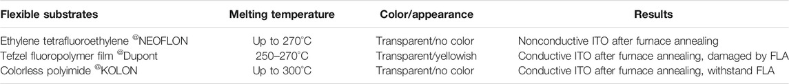
TABLE 1. Comparative analysis of the flexible substrate materials tested for ITO printing.
ITO ink was initially spin-coated at room temperature, with 3,500 rpm and 25 s rotation speed and duration, respectively, which results in 70 ± 7 nm thickness of the ITO layer. Five ITO samples were investigated with the use of a scanning electron microscope (SEM) to determine the thickness. CPI films with a size of 2.5 × 2.5 cm were used as substrates attached to a glass slide for uniform spin-coating and printing. Oxygen plasma cleaning using Diener Atto Plasma System (10 sccm gas flow rate and 50% power generation) for 2 min to improve surface wettability of CPI films was performed during the next step. After the spin-coating step, ITO layers were annealed at a constant temperature (series of samples annealed at 215, 230, and 250°C) under a low vacuum condition of 0.1 Pa for 1 h. Meyer Burger PixDRO LP50 inkjet printer was used for inkjet printing of the ink using Dimatix disposable cartridges with 10 pL nozzle volume. Inkjet-printed samples were annealed under the same low vacuum condition as for the spin-coated layers. The thickness of the ITO patterns was investigated for three printed samples and measured to be around 220 ± 12 nm.
Blue dye Sensidizer SQ2 (Solaronix) was used in this study. Sensidizer SQ2 was dispersed in ethanol to achieve 4.5 mM solution and then spin-coated during 15 s onto the annealed ITO patterns with 1,500 rpm rotation speed. A photonic curing system (NovaCentrix PulseForge 1,300) was used to perform FLA of the ITO patterns in the air atmosphere. SQ2 dye has a peak absorption at 600–650 nm, therefore, FLA applied on the dye-covered ITO layer results in effective light absorption and instant heating of the dye together with the underlying ITO layer. ITO patterns on CPI films were positioned under the xenon lamp of the FLA system. We have varied lamp voltage during the FLA process from 550 V (measured to be the lowest effective value) to 650 V, and pulse envelope—from 500 to 1,000 µs. The lowest lamp voltage—550 V allowed to achieve less than 25% relative sheet resistance change. The samples annealed under the highest 650 V lamp voltage lost their transparency due to the appearance of the undesired spots under too high temperatures reached on the surface. With the fixed values of pulse length and lamp voltage, we have varied the number of pulse repetitions. Five repetitions allowed to achieve around 60% relative sheet resistance change with no optical sample degradation. Thus, one pulse light lasting 900 µs comprised three micro pulses with ultrashort 30 µs break after each micropulse was repeated five times (20 J cm−2 total output energy density).
The SimPulse tool was used to estimate the temperatures reached on the surface of the ITO layer. It couples a transient 1-D heat conduction model to temperature-dependent thermal and optical material properties (Schroder, 2011). For the simulations of the temperature profiles 70 nm thick ITO film on 50 µm thick CPI film was selected as layers stack for the SimPulse tool. Temperature profiles for each FLA step described above are demonstrated in Figure 1, taking into account absorption of the bare ITO sample—(C) and corrected absorption with the dye layer—(D). It is assumed that during the annealing step, the average temperature on the ITO surface rises from 350 to 650°C due to the dye layer absorption.
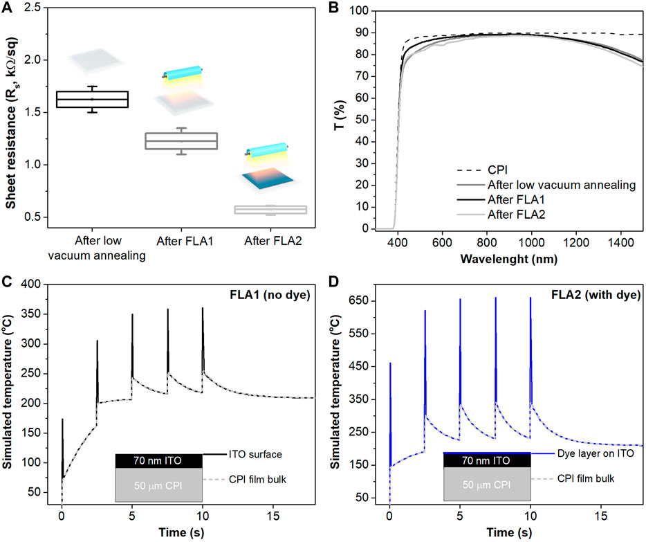
FIGURE 1. (A) Sheet resistance of the ITO patterns on CPI films after initial low vacuum annealing, after FLA1 and FLA2, (B) Optical transmittance curves of the CPI and CPI/ITO structures at different annealing stages. (C) Simulated temperature profiles obtained for the CPI/ITO structures during the FLA1 (no dye) process and (D) during the FLA2 process (with the dye).
The homemade flexing system we used consisted of two main parts, a bending machine and a measurement setup based on a measurement unit and a PC. The bending machine was a pneumatically driven moving plate system controlled by a specially made controller unit. Tested flexible ITO structures on CPI films were placed and attached between two parallel plates, which cause bending when moved. Bending tests were run with bending radii of 14 mm.
Thicknesses of the spin-coated and inkjet-printed ITO layers and the morphology of the samples were investigated and obtained using FEI Quanta 650 SEM. UV–vis spectrometer Shimadzu UV-3600 was used for the transmittance measurements from 250 to 1,500 nm taking air as the reference (baseline). Electrical properties were measured by the four-point probe device for the thin-film sheet resistance measurements.
Results and Discussion
ITO Patterns on CPI Film
Figure 2 schematically describes the fabrication steps of conductive invisible ITO patterns on flexible CPI film. After the initial cleaning step, O2 plasma treatment for 2 min was applied on the CPI substrate to obtain necessary wetting for the inkjet printing (Figure 2A). CPI film is then fixed flat on the glass support slide (Figure 2B). ITO nano ink is inkjet-printed on the CPI film. The as-printed ITO films are brown and nonconductive (Figure 2C), which is explained by the presence of the cyclododecene solvent and ink stabilizers. After the low vacuum annealing for 1 h under the constant temperature (Figure 2D), the precursor ITO film becomes transparent and conductive. To improve the initial optical and electrical properties of the ITO film, it is processed with FLA—called FLA1 (Figure 2E). It is essential to apply the initial low vacuum annealing step before FLA1 since the energy and duration of the millisecond long pulses of the FLA would not be enough for the effective ITO nanoparticles sintering within the accessible (less than 500) amount of pulses applied. Next, blue Sensidizer SQ2 dye dispersed in ethanol is spin-coated onto the annealed ITO film (Figure 2F). ITO film with the dye layer is then processed again with FLA—called FLA2 (Figure 2G). For the FLA1 and FLA2, identical pulse and lamp voltage conditions were used as described in the Materials and Methods section. After the FLA2 step, the flexible CPI film with processed ITO structure is peeled off from the glass support (Figure 2H). ITO becomes transparent again (Figure 2I) since the dye layer decomposes during the FLA under the high temperature reached on the surface. Scanning electron microscopy (SEM) image (Figure 2J) reveals uniformly sintered ITO film morphology. The detailed experimental conditions are described in the Materials and Methods Section.
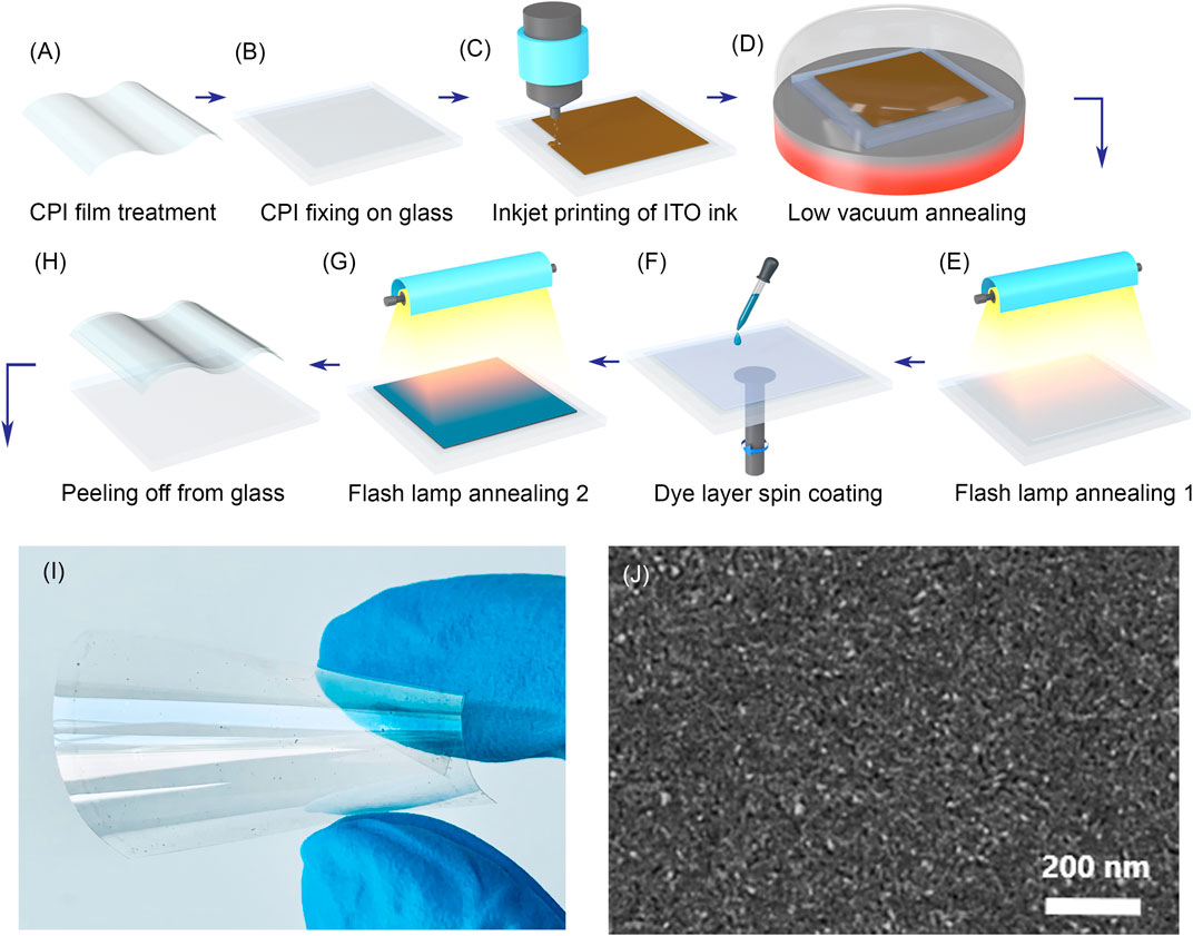
FIGURE 2. Schematic illustration of the fabrication process: (A) cleaning and treatment of CPI substrate; (B) fixing of the CPI film on glass support slide; (C) inkjet printing of the ITO nano ink on CPI film; (D) vacuum annealing of ITO film in the furnace; (E) flash lamp annealing (FLA1) of the obtained transparent ITO; (F) spin-coating of blue dye onto the annealed ITO film; (G) flash lamp annealing of the ITO film with the dye layer (FLA2); (H) peeling off the processed ITO layer on CPI film from glass. (I) Sample photograph of printed ITO on the CPI film and (J) SEM image of the sintered ITO pattern.
Figure 1A shows the sheet resistance values of the ITO films at different stages of the applied annealing process. The FLA1 step applied to the ITO film after low vacuum annealing results in a sheet resistance decrease, indicating the conductivity improvement due to the sufficient heating of the ITO film during FLA1. Next, FLA2 applied onto the dye-coated ITO film results in the sheet resistance decrease by more than a factor of two from the initial value. In this series of experiments, ITO patterns were annealed at 250°C during the initial low vacuum annealing stage. The 70 ± 7 nm thick ITO on CPI film has a transmittance (T%) of 80–90% in the wavelength range of 380–1,100 nm (Figure 1B). The transmittance of the ITO structure in the visible range after FLA1 is lowered by 2% after the low vacuum step (black line for low vacuum annealed ITO compared to the light grey line—for ITO after FLA1). The emission spectrum of the xenon lamp has a broad peak in the visible region (400–800 nm), at the same time, SQ2 dye has a peak absorption at 600–650 nm; therefore, FLA2 applied on the dye-covered ITO layer results in effective light absorption and instant heating of the dye together with the underlying ITO layer. Thermal decomposition and evaporation of the fully organic dye decomposition products take place. To prove this assumption that higher temperatures are obtained on the surface of the ITO film in the case of FLA2 applied on the dye layer, we carried out the temperature simulations by SimPulse software. Based on the simulations (Figures 1C,D), in the case of SQ2 dye on top of the ITO during the FLA surface temperature of the ITO film elevates from 360 up to 650°C during FLA pulses, which is effective enough for the sintering of ITO nanoparticles (Hong et al., 2011). It is essential to highlight that during the FLA processes, the CPI substrate remains relatively cold—below the melting point, as shown by the grey dashed lines (Figures 1C,D), which is the main advantage of the FLA method.
Variation of the Annealing Temperature and Flexibility Tests
Based on the differential scanning calorimetry (DSC) curve, 250°C was selected previously as an optimal annealing temperature for the low vacuum annealing step of ITO film printed on rigid glass (Gilshtein et al., 2020). However, such thermal annealing requirements limit the flexible substrate choice, which has to be at the same time mechanically stable and transparent. Since the initial low vacuum annealing step is essential and defines the starting electrical properties of the ITO layer, we have optimized this step by varying vacuum annealing temperatures for the ITO fabricated on CPI film. Figure 3A shows sheet resistance of the ITO films as a function of the annealing temperature applied during low vacuum annealing. A decrease in the annealing temperature from 250 to 230°C results in reducing sheet resistance by 60% immediately after the furnace annealing. However, a further decrease from 230 to 215°C does not help to reduce the electrical resistance of the ITO on CPI film. It may be due to the lower temperature compared to the one needed to decompose the solvent and remove organic impurities for proper sintering of ITO nanoparticles. Figure 3A shows that the FLA1 step results in a resistance drop—60% from the initial value—and the FLA2 step—40% from the initial value. The effect of FLA1 and FLA2 steps will be described in more detail in the next part.
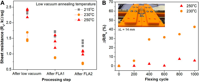
FIGURE 3. (A) Sheet resistance values of the ITO films on CPI substrate annealed at various temperatures during the initial low vacuum annealing step shown for all the following processing steps; (B) Resistance change for the ITO on CPI film initially annealed at 230 and 250°C measured during flexibility fatigue tests.
The mechanical and electrical stability of the ITO layers on CPI films was analyzed through the flexibility fatigue tests (Figure 3B). Bending tests were run with bending radii of 14 mm. We aimed to submit the structures to at least 1,000 bendings to confirm the feasibility of flexible ITO applications. The ITO structure annealed at 250°C demonstrated better electrical stability under flexing tests (less than 8% in resistance degradation after 1,000 mechanical cycles) than the ITO annealed at 230°C (more than 40%).
Application of Invisible ITO Patterns in a Flexible Security System
To utilize the unique feature of ITO patterns invisibility, the security access system was assembled. The Block diagram of the security lock system is shown in Figure 4A. Inkjet printing of the ITO ink was performed with a Meyer Burger PixDRO LP50 inkjet printer using cartridges with 10 pL nozzle volume to print ITO structures uniformly over large areas on CPI films. To demonstrate the working principle of the device, the number of working electrodes is reduced to four. Four square-shaped patterns were designed for inkjet printing, acting as the invisible buttons (Figure 4B). Next, conductive tape electrodes were connected to the printed and processed ITO patterns for the wiring, and CPI film was attached to the door, as shown in Figure 4C. The device demonstrates the sensing operation principles based on the multiple touchpoints of transparent capacitive ITO sensors. Each of the four ITO electrodes is assigned to the corresponding numbers "1, 2, 3, and 4″ using microcontroller unit programming. The first four digits of the number "π" are set as the access code for the demonstrated security system, with the value of “3.141” (Figure 4D).
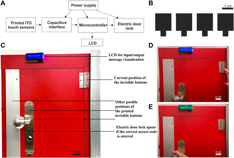
FIGURE 4. Transparent and conductive ITO patterns application in a flexible security system. (A) Block diagram of the security lock system; (B) The patterns of invisible touch buttons for inkjet printing. (C) The CPI film with printed and annealed ITO buttons is attached to the door and integrated into the security system. (D) When the patterns are touched in a preset order, the “Access Granted” messages appear (E), and the door is opened.
Consequently, pressing the ITO electrodes by the user's finger—No3, No1, No4, and No1—the user receives immediate feedback through the LCD, displaying messages such as "Access Granted" (Figure 4E). In the wrong sequence of the pressed ITO electrodes, the message "Access Denied" will appear on the screen. The detailed operation principles are demonstrated in Supplementary Video. The active touch-part of the device utilizes high transmittance values—up to 85% in the visible range—which makes it hard for the human eye to distinguish where the sensing part is located and, at the same time, increases the security level offered by the device.
Conclusion
Printed conductive and transparent ITO patterns on flexible colorless polyimide substrates are fabricated using the flash lamp annealing and a light-absorbing dye layer. Higher surface temperatures are obtained through the dye layer, enabling the sintering of ITO nanoparticle-based layers without destroying the underlying CPI film. At the same time, ITO patterns on CPI films initially annealed at 230°C demonstrate the lowest sheet resistance value of 520 Ω/sq for 70 nm ITO thickness. The inkjet-printed ITO film annealed at 250°C and processed with the FLA demonstrate better electrical stability after 1,000 bending cycles with less than 8% resistance degradation than the ITO annealed at 230°C. Inkjet-printed and FLA-processed transparent ITO structures can be integrated into sensors, solar cells, thin-film transistors, light-emitting diodes, and other devices where flexibility and transparency of the electrodes are required. The electrodes can be utilized for the access control systems with additional security levels due to the invisibility of such setups. The demonstrator based on flexible, printed, and transparent ITO patterns fabricated in this study can be used along with the existing security systems by the organizations that require multilevel security, such as banks, business corporations, the military, and hospitals. In all the listed cases, only a limited number of people will know the access password and the location of touch buttons since for the person who is not familiar with the system, it is entirely invisible.
Data Availability Statement
The raw data supporting the conclusion of this article will be made available by the authors, without undue reservation.
Author Contributions
EG and YR were responsible for the conceptualization of the project idea. EG, JT, and YR formulated the overarching research goals and aims. JT performed experimental steps related to the ITO ink spin-coating and annealing. JT performed UV–Vis spectroscopy measurements, electrical properties characterization, and flexibility tests. EG conducted the SEM studies and performed the temperature profile simulation; EG and JT performed photonic sintering experiments. SB performed the inkjet printing of ITO ink for the invisible buttons. GS designed and fabricated the prototype of the security system with the electric door lock. EG evaluated the produced research data and prepared the main manuscript. EG was responsible for visualization and data presentation in the published work. The manuscript was reviewed and accepted by all authors. EG and YR supervised the experimental progress.
Funding
The EMPAPOSTDOCS-II program has received funding from the European Union’s Horizon 2020 research and innovation program under the Marie Sklodowska-Curie Grant Agreement Number 754364. The authors gratefully acknowledge financial support from the Strategic Focus Area Advanced Manufacturing of the ETH domain under the project FOXIP—Functional OXIdes Printed on Polymers and Paper.
Conflict of Interest
The authors declare that the research was conducted in the absence of any commercial or financial relationships that could be construed as a potential conflict of interest.
References
An, B. W., Heo, S., Ji, S., Bien, F., and Park, J.-U. (2018). Transparent and Flexible Fingerprint Sensor Array with Multiplexed Detection of Tactile Pressure and Skin Temperature. Nat. Commun. 9. doi:10.1038/s41467-018-04906-1
Chen, W., and Yan, X. (2020). Progress in Achieving High-Performance Piezoresistive and Capacitive Flexible Pressure Sensors: A Review. J. Mater. Sci. Tech. 43, 175–188. doi:10.1016/j.jmst.2019.11.010
Chen, Z., Li, W., Li, R., Zhang, Y., Xu, G., and Cheng, H. (2013). Fabrication of Highly Transparent and Conductive Indium-Tin Oxide Thin Films with a High Figure of Merit via Solution Processing. Langmuir 29, 13836–13842. doi:10.1021/la4033282
Datta, R. S., Syed, N., Zavabeti, A., Jannat, A., Mohiuddin, M., Rokunuzzaman, M., et al. (2020). Flexible Two-Dimensional Indium Tin Oxide Fabricated Using a Liquid Metal Printing Technique. Nat. Electron. 3, 51–58. doi:10.1038/s41928-019-0353-8
Fang, M., Aristov, A., Rao, K. V., Kabashin, A. V., and Belova, L. (2013). Particle-free Inkjet Printing of Nanostructured Porous Indium Tin Oxide Thin Films. RSC Adv. 3, 19501–19507. doi:10.1039/C3RA40487K
Gilshtein, E., Bolat, S., Sevilla, G. T., Cabas‐Vidani, A., Clemens, F., Graule, T., et al. (2020). Inkjet‐Printed Conductive ITO Patterns for Transparent Security Systems. Adv. Mater. Technol. 5, 2000369. doi:10.1002/admt.202000369
Hong, S.-J., Kim, J.-W., and Han, J. I. (2011). Improvement of Electrical Properties of Printed ITO Thin Films by Heat-Treatment Conditions. Curr. Appl. Phys. 11, S202–S205. doi:10.1016/j.cap.2010.11.081
Hwang, M.-s., Jeong, B.-y., Moon, J., Chun, S.-K., and Kim, J. (2011). Inkjet-printing of Indium Tin Oxide (ITO) Films for Transparent Conducting Electrodes. Mater. Sci. Eng. B 176, 1128–1131. doi:10.1016/j.mseb.2011.05.053
Jeong, J.-A., Lee, J., Kim, H., Kim, H.-K., and Na, S.-I. (2010). Ink-jet Printed Transparent Electrode Using Nano-Size Indium Tin Oxide Particles for Organic Photovoltaics. Solar Energ. Mater. Solar Cells 94, 1840–1844. doi:10.1016/j.solmat.2010.05.052
Kang, M., Kim, J., Jang, B., Chae, Y., Kim, J.-H., and Ahn, J.-H. (2017). Graphene-Based Three-Dimensional Capacitive Touch Sensor for Wearable Electronics. ACS Nano 11, 7950–7957. doi:10.1021/acsnano.7b02474
Khanna, A., and Kaur, S. (2020). Internet of Things (IoT), Applications and Challenges: A Comprehensive Review. Wireless Pers Commun. 114, 1687–1762. doi:10.1007/s11277-020-07446-4
MacDonald, W. A., Looney, M. K., MacKerron, D., Eveson, R., Adam, R., Hashimoto, K., et al. (2007). Latest Advances in Substrates for Flexible Electronics. J. Soc. Inf. Display 15, 1075. doi:10.1889/1.2825093
Ni, H.-j., Liu, J.-g., Wang, Z.-h., and Yang, S.-y. (2015). A Review on Colorless and Optically Transparent Polyimide Films: Chemistry, Process and Engineering Applications. J. Ind. Eng. Chem. 28, 16–27. doi:10.1016/j.jiec.2015.03.013
Park, J.-H., Kim, C.-H., Lee, J.-H., and Kim, H.-K. (2021). Transparent and Flexible SiOC Films on Colorless Polyimide Substrate for Flexible Cover Window. Micromachines 12, 233. doi:10.3390/mi12030233
Ravindra, Y. N., and Konda, R. B. (2020). GSM Based Security Lock Using Linear Actuator. Int. J. Scientific Res. Sci. Tech. 7 (2), 356–359. doi:10.32628/ijsrst207266
Rebohle, L. (2019). “The Technology of Flash Lamp Annealing,” in Flash Lamp Annealing: From Basics to Applications. Editors R. Hull, C. Jagadish, Y. Kawazoe, R. M. Osgood, J. Parisi, U. W. Pohlet al. (Cham: Springer International Publishing), 15–70. doi:10.1007/978-3-030-23299-3_2
Schroder, K. A. (2011). Mechanisms of Photonic curingTM: Processing High Temperature Films on Low Temperature Substrates. Technical Proceedings of the 2011 NSTI Nanotechnology Conference and Expo. Nsti-nanotech 2011, Boston, Mass, USA, 13–16 Jun 2011 2, 220–223.
Serkov, A. A., Snelling, H. V., Heusing, S., and Amaral, T. M. (2019). Laser Sintering of Gravure Printed Indium Tin Oxide Films on Polyethylene Terephthalate for Flexible Electronics. Sci. Rep. 9. doi:10.1038/s41598-018-38043-y
Tawalbeh, L. a., Muheidat, F., Tawalbeh, M., and Quwaider, M. (2020). IoT Privacy and Security: Challenges and Solutions. Appl. Sci. 10, 4102–4117. doi:10.3390/APP10124102
Tue, P. T., Inoue, S., Takamura, Y., and Shimoda, T. (2016). Combustion Synthesized Indium-Tin-Oxide (ITO) Thin Film for Source/drain Electrodes in All Solution-Processed Oxide Thin-Film Transistors. Appl. Phys. A. 122, 623. doi:10.1007/s00339-016-0156-y
Wang, X., Zhang, H., Dong, L., Han, X., Du, W., Zhai, J., et al. (2016). Self-Powered High-Resolution and Pressure-Sensitive Triboelectric Sensor Matrix for Real-Time Tactile Mapping. Adv. Mater. 28, 2896–2903. doi:10.1002/adma.201503407
Keywords: capacitive touch sensors, flash lamp annealing, indium tin oxide, inkjet printing, transparent electrodes, flexible electronics
Citation: Gilshtein E, Tacneng J, Bolat S, Torres Sevilla G and Romanyuk YE (2021) Invisible and Flexible Printed Sensors Based on ITO Nanoparticle Ink for Security Applications. Front. Nanotechnol. 3:700539. doi: 10.3389/fnano.2021.700539
Received: 26 April 2021; Accepted: 02 July 2021;
Published: 14 July 2021.
Edited by:
Isabelle Huynen, Catholic University of Louvain, BelgiumReviewed by:
Yongkuk Lee, Wichita State University, United StatesHee-Seok Kim, University of Washington Tacoma, United States
Copyright © 2021 Gilshtein, Tacneng, Bolat, Torres Sevilla and Romanyuk. This is an open-access article distributed under the terms of the Creative Commons Attribution License (CC BY). The use, distribution or reproduction in other forums is permitted, provided the original author(s) and the copyright owner(s) are credited and that the original publication in this journal is cited, in accordance with accepted academic practice. No use, distribution or reproduction is permitted which does not comply with these terms.
*Correspondence: Evgeniia Gilshtein, ZXZnZW5paWEuZ2lsc2h0ZWluQGVtcGEuY2g=