 Andre Zeumault
  Shamiul Alam
  Zack Wood 1
 Ahmedullah Aziz
  Garrett S. Rose
 - 1Min H. Kao Department of Electrical Engineering and Computer Science, The University of Tennessee, Knoxville, TN, United States
- 2Department of Materials Science and Engineering, The University of Tennessee, Knoxville, TN, United States
In neuromorphic computing, memristors (or “memory resistors”) have been primarily studied as key elements in artificial synapse implementations, where the memristor provides a variable weight with intrinsic long-term memory capabilities, based on its modifiable resistive-switching characteristics. Here, we demonstrate an efficient methodology for simulating resistive-switching of HfO2 memristors within Synopsys TCAD Sentaurus—a well established, versatile framework for electronic device simulation, visualization and modeling. Kinetic Monte Carlo is used to model the temporal dynamics of filament formation and rupture wherein additional band-to-trap electronic transitions are included to account for polaronic effects due to strong electron-lattice coupling in HfO2. The conductive filament is modeled as oxygen vacancies which behave as electron traps as opposed to ionized donors, consistent with recent experimental data showing p-type conductivity in HfOx films having high oxygen vacancy concentrations and ab-initio calculations showing the increased thermodynamic stability of neutral and charged oxygen vacancies under conditions of electron injection. Pulsed IV characteristics are obtained by inputting the dynamic state of the system—which consists of oxygen ions, unoccupied oxygen vacancies, and occupied oxygen vacancies at various positions—into Synopsis TCAD Sentaurus for quasi-static simulations. This allows direct visualization of filament electrostatics as well as the implementation of a nonlocal, trap-assisted-tunneling model to estimate current-voltage characteristics during switching. The model utilizes effective masses and work functions of the top and bottom electrodes as additional parameters influencing filament dynamics. Together, this approach can be used to provide valuable device- and circuit-level insight, such as forming voltage, resistance levels and success rates of programming operations, as we demonstrate.
1 Introduction
In recent years, memristor devices have shown great potential for neuromorphic computing due to their resistive-switching dynamics and electrical behavior resembling that of biological synapses (Chua, 1971; Xia and Yang, 2019; Strukov et al., 2008). Memristors are resistors with memory whose resistance level can be controlled either through an applied voltage (i.e., flux-linkage) or current (i.e., charge-fluence). Oxide memristors tend to be voltage-controlled, having a metal-oxide-metal device structure identical to a parallel-plate capacitor. Since the oxide thickness tends to be thin (∼ 2–5 nm) (Pi et al., 2019) and the switching speed can be very fast (<1 ns) (Choi et al., 2016), a small amount of energy is required for programming resistance states. With these unique features, in addition to non-volatility, they have shown the great promise for building energy and area efficient memristive crossbar arrays (1T1R arrays) to form neural networks for a wide range of applications including robotics, computer vision, and speech recognition (Yao et al., 2017; Li et al., 2018b,a; Hu et al., 2016). A 1T1R crossbar array (Figure 1A) offers added benefits due to the use of a transistor in each resistive RAM (RRAM) memory cell. The transistor plays a major role in mitigating the sneak current path and programming disturbance associated with resistive (i.e., 1R) crossbar arrays (Manem et al., 2012; Yao et al., 2015). Furthermore, the transistor’s gate terminal in the 1T1R cell allows for better control over the current through the memristive device. It also provides more resilience to the switching voltage magnitude and attains better uniformity (Liu et al., 2014).
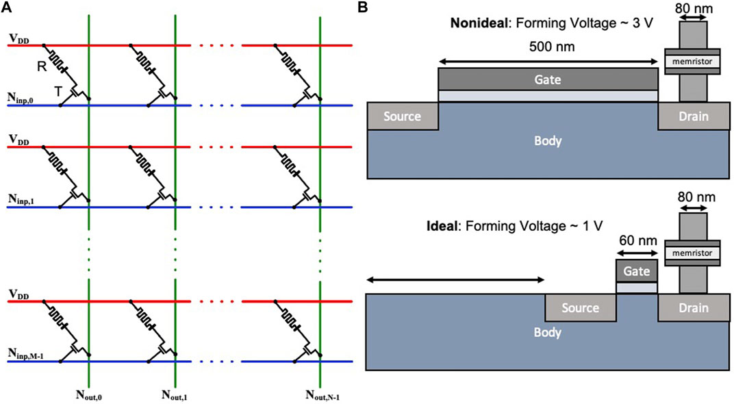
FIGURE 1. (A) A M × N crossbar array of one-transistor, one-memristor (1T1R) devices for neuromorphic applications. (B) Illustration of the size of transistors needed for memristors having high and low forming voltages.
Electroforming, a one-time forming or initialization process, is often required in transition metal oxide (TMO) memristors (Strukov et al., 2008), which have been widely used for memristive crossbar arrays, including those used in neuromorphic systems. However, for forming, the voltage often needs to be higher than the nominal supply voltage of modern CMOS processes, which causes significant design and integration challenges (Amer et al., 2017b,a). Memristors with high forming voltages require dedicated circuitry capable of tolerating such high voltage levels for executing the in-field forming. Furthermore, the area constraints associated with the in-field forming circuitry undermines the density benefits of the crossbars. In addition, such transistors are generally large compared to the regular devices to accommodate these high forming voltages (Figure 1B). For example, for a 65 nm CMOS process (Beckmann et al., 2016; Amer et al., 2017a) used to prepare 80 nm × 80 nm memristor areas, the minimum length of the transistor used in the 1T1R cell could be as much as 0.5 μm to endure forming voltages up to 3.3 V. In contrast, the minimum length of the regular transistor used for peripheral circuitry is 60 nm with the nominal voltage 1.2 V or 1.0 V, depending on the process. Thus, researchers have focused on lowering the forming voltages to a level of operation that allows for better exploitation of memristive crossbar density (Govoreanu et al., 2011; Koveshnikov et al., 2012; Huang et al., 2013a; Chen, 2013; Kim et al., 2016; Amer et al., 2017c).
The electroforming process, in addition to reset and set operations, can be simulated from a condensed set of rate equations that define all possible changes of state of the system using Kinetic Monte Carlo (KMC). Rate equations used to model filament dynamics are typically based on the following physical transitions: oxygen ion (i.e., O2−) and vacancy (i.e.,
Despite growing evidence to the contrary, few modelling approaches allow the charge state of the oxygen vacancy (i.e., +2) to change during forming. In effect, oxygen vacancies are modeled as fixed charges for the purpose of determining filament evolution, yet as electron traps for the purpose of calculating current, which is based on nonlocal multiple-phonon trap-assisted tunneling in which trap occupancy dynamics is fundamentally important. This inconsistency greatly limits the utility of existing approaches to provide increased physical insight into HfOx switching behavior–beyond that which existing compact models already provide (Bianchi et al. (2020); Yu and Wong (2010); Huang et al. (2013b); Guan et al. (2012b); Jiang et al. (2014))–which can be extended to device design, circuits and systems-level refinements (e.g., reducing forming voltage). The assumption of a static positive charge contradicts experimental evidence showing p-type conductivity in highly defective HfOx films (Hildebrandt et al., 2011)—suggesting that oxygen vacancies are deep acceptor-like traps (>3 eV from the conduction band edge). Moreover, ab-inito calculations have shown the thermodynamic stability of neutral and negatively charged vacancy states increases in conditions of electron injection (i.e., current flow) due to electron capture (Bradley et al., 2015). This is consistent with experimental work using in-situ TEM electron holography and EELS in which oxygen-vacancy filaments were observed, spatially, as regions of negative space-charge (Li et al., 2017). Unlike previous KMC approaches, together these observations are, in fact, self-consistent with the physical assumptions used to model current flow in HfO2 based memristive devices, in which, conduction occurs through a nonlocal, trap-assisted tunneling process involving electron capture and emission—appropriate for insulators having point defects (e.g., TaOx, HfOx, ZrOx, NbOx).
Here, using a simple 2D model, we show that, in addition to the conventional set of rate equations (i.e., Frenkel pair generation/recombination and diffusion) filament evolution in HfOx can be modeled self-consistently as the result of band-to-trap electron capture and emission processes between the electrodes and oxygen vacancies (Figure 2). In this way, the conductive filament consists of occupied oxygen vacancy electron traps, which lower their energy upon electron capture due to strong coupling between ionized defects and the lattice in HfOx (Huang-Rhys factor, S = 17) as depicted in Figure 2. The primary benefit in this approach is that additional parameters associated with the electrodes (e.g., work function, effective mass) and those of the oxygen vacancy states (e.g., trap energy level, capture cross-section, thermal barrier and binding energy) are intimately linked to resistive switching behavior, as we show. Not only do these additional parameters provide more depth in terms of physical insight and modeling capability, they are readily accessible experimentally or through ab-initio estimates. Using TCAD Sentaurus (Synopsys, 2019), we demonstrate that the common forming, reset and set characteristics can be successfully reproduced and visualized. In particular, we show that certain regions within the filament have a negative potential–stemming from a negative space charge due to electron capture. This is consistent with recent experimental work describing the filament as a negative potential synapse (Li et al., 2017). Next, we couple our device model with a phenomenological compact model to bring in physics-based insights to the circuit-level simulation of a memristor-based synapse topology. Finally, to underscore the unique strength of our model, we investigate a device-circuit co-design strategy powered by Monte-Carlo simulations with different levels of initial oxygen vacancy volume faction.
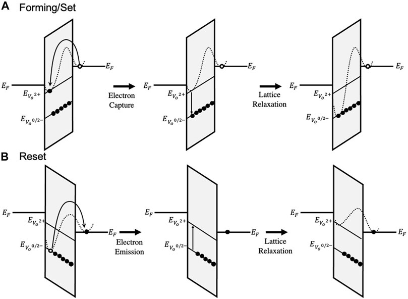
FIGURE 2. Depiction of electron capture and emission as band-to-trap and trap-to-band, respectively for a trap located below the Fermi level of the cathode (i.e. ΔETF < 0). (A) The forming and set process is facilitated by electron capture and lattice relaxation. (B) The reset process is facilitated by electron emission and lattice relaxation.
2 Methods
2.1 Material Specifications and Device Geometry
A complete list of parameters used to specify the HfO2 layer are provided in Table 1. Of these, the parameters related to hafnium-oxygen bond energy and polarization were obtained from the thermochemical model (McPherson et al., 2003), assuming a 100% monoclinic phase composition. This makes clear the assumptions regarding crystalline phase of the HfO2 thin film and the activation enthalpy required for breaking the hafnium-oxygen bond–which differs due to differences in polarization and the number of bonds required to be broken about the Hf central atom. It should be noted that, in practice, a mixture of monoclinic and tetragonal phases are present in varying ratios–the monoclinic phase has a nominal breakdown field of 6.7 MV cm−1 whereas the tetragonal phase has a breakdown field of 3.9 MV cm−1 (McPherson et al., 2003). Empirically, the breakdown field is found to vary between 3 and 5 MV cm−1 (Sire et al., 2007) for atomic layer deposition (ALD) grown HfO2 films on TiN of comparable thickness used in this work.
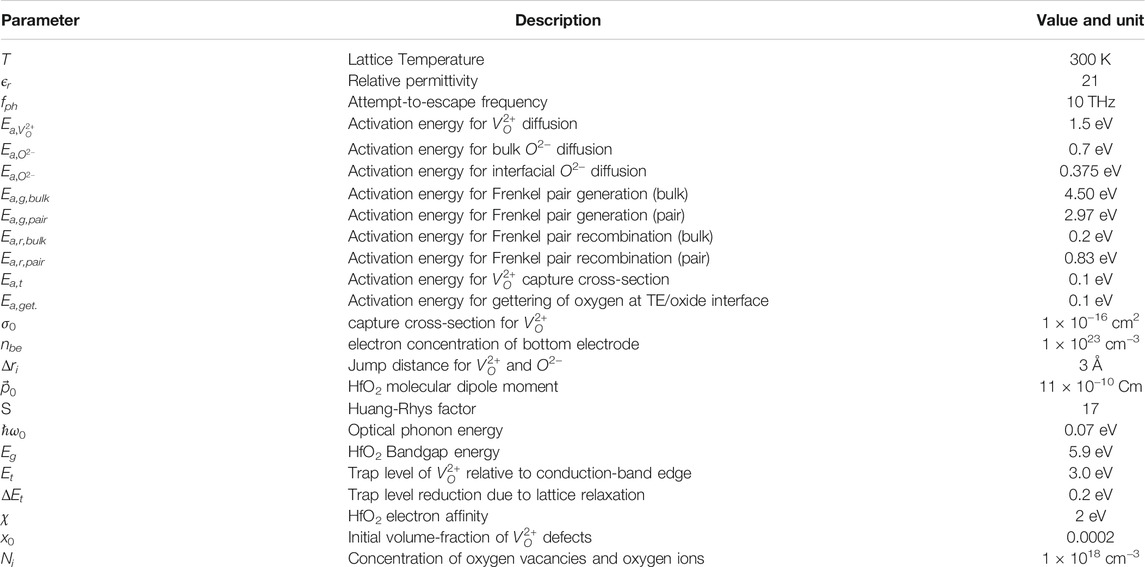
TABLE 1. Summary of nominal materials parameters used in this work unless otherwise stated.
As indicated in Figure 3A, the memristor is modeled as a two-dimensional top-electrode (TE)/HfOx/bottom-electrode (BE) structure on a square grid. The HfOx thickness is 5 nm and the device width is 40 nm. The Ti (TE) and TiN (BE) electrodes are modeled as ideal, Ohmic contacts with a 0 Ω series resistance. The work function of the Ti and TiN layers were set to 4.33 and 4.5 eV respectively. The electron effective masses of the Ti and TiN layers were set to 3.2 and 2.0 respectively according to literature (Lima et al., 2012). Following the lattice-gas model, a grid point represents the smallest physical unit considered by this simulation, capable of representing either an empty “site” (for diffusion or the formation of a Frenkel pair), a positively charged oxygen vacancy (
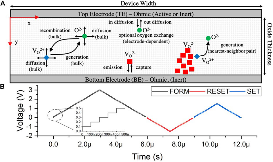
FIGURE 3. (A) Illustration showing device geometry and description of the processes modeled using Kinetic Monte Carlo. (B) Example voltage waveform used to perform forming, reset, and set operations in sequence using a stepped voltage ramp with a KMC simulation time of 100 ns. The resulting state of the system at the end of each voltage increment is used as input to Synopsys TCAD Sentaurus.
The initial state of the system can be defined by randomizing the location of oxygen vacancies and oxygen ions (needed to ensure charge-neutrality)–to represent an amorphous film. Alternatively, since it is known that ALD-deposited HfO2 thin films exhibit a columnar grain morphology (≈8 nm grain size (Ho et al., 2003)), oxygen vacancies can be placed along grain boundaries due to the reduced formation energy–to represent a polycrystalline film. The initial concentration of vacancies is determined by a variable volume fraction parameter which we nominally set to 0.0002 (i.e., 0.02 at. %). Our focus here is to demonstrate the key differences and advantages of our physical model incorporating additional electronic transitions to the constitutive rate equations describing filament dynamics and its implementation in TCAD Sentaurus.
2.2 Filament Evolution Under Voltage Stress
Filament evolution during forming, set and reset operations are described using a simple set of rate equations corresponding to the following physical processes, as outlined in Table 2:
• Electron capture or emission by oxygen vacancies
• Oxygen vacancy and ion diffusion
• Frenkel pair generation and recombination (isolated bulk and nearest neighbor pairs)
• Oxygen gettering by Ti
TABLE 2. Summary of transitions rates modelled using Kinetic Monte Carlo procedure and their parameters. Lattice coordinates are listed as relative positions to a given lattice point at (i, j) following the convention of the lattice gas model (Jansen, 2012). * = site, O2− = oxygenion,
These processes are implemented via a classical KMC selection algorithm applied to a chosen initial state of the system (top electrode, bottom electrode, oxygen ion, oxygen vacancy and filament), and updated in time according to Poisson statistics and the time scale of each selected mechanism. The details of the dynamical monte carlo algorithm and the meaning of simulation time (Fichthorn and Weinberg, 1991), and its application to the formation of 2D/3D conductive filaments (metallic and oxygen vacancy) has been discussed elsewhere (Sementa et al., 2017; Aldana et al., 2018, 2020; Loy et al., 2020). Here, we provide a minimal outline of the essential aspects, assumptions and parameters of the rate equations we’ve implemented. In particular, we highlight the physical assumptions that establish consistency between phenomenological models of filament evolution and models of electric conduction—needed for efficient and accurate device-circuit co-design.
2.2.1 Filament Changes Mediated by Electron Capture/Emission
We model filament precipitation (dissolution) as the net result of Frenkel pair generation (recombination) and electron capture (emission) by oxygen vacancy electron traps. For simplicity, we couple oxygen vacancy traps to the conduction band in the bottom-electrode, which permits straightforward evaluation of rate equations within the electron trap picture. Conventionally, capture and emission rates are defined in terms of a thermally activated capture-cross section, a tunneling coefficient, and a field-dependent trap barrier that depends on the relative energy difference between the trap level and the Fermi level of the bottom electrode. In other words, the forming, set and reset operations are described as band-to-trap (or trap-to-band) electronic transitions within the Wentzel-Kramers-Brillouin (WKB) approximation Eqs 1–3.
These expressions are derived in the Supplementary Material. Here, yt represents the y-coordinate of the trap relative to the electrode, y0 is a parameter related to the wavefunction overlap between the electronic state in the trap and in the electrode. Within the WKB approximation, after applying the triangular barrier approximation for the bands we have the following:
The quantity Φbe − χox represents the conduction band offset between the bottom electrode and the oxide, in terms of the work function of the bottom electrode Φbe and the electron affinity of the oxide χox.
In Eqs 1–3, it is assumed that the electric field has a symmetric influence on transition rates, that is, the barrier lowering in the forward direction is equal and opposite that of the reverse in order to maintain steady-state equilibrium. The case statements in Eqs 1, 2 exist since the trap may be higher (i.e., Etf > 0) or lower (Etf < 0) than the Fermi level in the bottom electrode. Parameters which depend on the bottom electrode are the electron concentration, nbe and the effective-mass,
We note that the time scale of electron capture and emission depends on the product of the carrier concentration in the electrodes, the thermal velocity and the capture cross section of oxygen vacancies as shown in Eqs 1–3 through a common exponential prefactor. Using values listed in Table 1, the ratio of the exponential prefactors for electronic (σ0nBEvth) and atomic processes (fph) is evaluated to be 8.25, so electronic processes are expected to occur much faster than atomic ones. However, the rate of electronic transitions also depends on the local electric field and the position of the trap relative to the electrode and so the above estimate only reflects those traps that are close to the bottom electrode. Therefore, the relative rates of electronic and atomic processes are expected to differ (generally reducing) as one moves from the BE to the TE under forming/set and from the TE to the BE under reset due to the change in voltage polarity.
The initial system consists of the electrodes and an initial concentration of positively charged, unoccupied oxygen vacancies. It should be noted that, although we have assumed a +2 charge state, the +2 oxygen vacancy is unstable in the presence of interstitial oxygen and/or conditions of electron injection. This is supported by ab-initio calculations suggesting that Frenkel pairs stabilize through the formation of neutral and/or negatively charged oxygen vacancies—facilitated by electron capture (Bradley et al., 2015). Experimentally, this is supported by the observation of p-type conductivity in highly defective HfOx films, suggesting that oxygen vacancies interact and stabilize as deep acceptors (Hildebrandt et al., 2011) as opposed to shallow donors. Thus, the formation of conductive oxygen vacancy filaments can be regarded as thermodynamically driven by the increase in binding energy due to electron capture of single vacancies and expected to subsequently stabilize due to defect aggregation (i.e. filament growth). We account for these effects by lowering the energy level of an oxygen vacancy, Et upon electron capture, by an amount equal to the increase in binding energy of neutral and negatively charged vacancies (≈0.2–0.9 eV) as predicted by ab-initio calculations (Bradley et al., 2015; Sementa et al., 2017). In general, this is a lattice relaxation process involving the emission/absorption of multiple phonons as described by several authors (Englman and Jortner, 1970; Henry and Lang, 1977; Nasyrov et al., 2004; Nasyrov and Gritsenko, 2011). Here, for simplicity, we assume the lattice relaxation coincides with electron capture (or emission). The assumed electron capture and emission processes are illustrated in Figure 2.
The significance of this model of filament growth is that it is more consistent with the nonlocal trap-assisted tunneling processes associated with electron conduction, which we later implement in TCAD Sentaurus to calculate the current-voltage characteristics as a more rigorous extension of these assumptions.
2.2.2 Oxygen Ion and Vacancy Diffusion
The rate of diffusion of oxygen ion and oxygen vacancy species is described as an Arrhenius Eq. 6. Here, the important parameters are the thermal barrier, ionic charge, and jump distance for each diffusing species.
2.2.3 Frenkel Pair Generation
Oxygen vacancy formation is achieved through the production of Frenkel pairs, requiring the breaking of metal-oxygen bonds. A thermochemical description of dielectric breakdown exists (McPherson et al., 2003), in which the activation energy for breakdown is lowered by the local electric field projection along a polarizable bond axis. This expression is common in describing dielectric breakdown in thin insulators and is common in oxide-reliability studies Eq. 7.
Within this model, breakdown is expected to begin at an electric field that lowers the effective thermal barrier to zero.
The value of Ea,g determines the minimum voltage needed for forming, and is therefore an important consideration for the design of memristor circuits, as previously discussed. Using typical values for HfO2 (p0 = 11 × 10−10 Cm, Ea,g = 4.5 eV, ϵr = 21), the breakdown field
2.2.4 Frenkel Pair Recombination
As previously discussed, upon formation, charged Frenkel pairs in HfO2 are unstable, requiring additional electrons from the conduction band to neutralize the oxygen vacancy and prevent rapid recombination. It is therefore expected that the thermal barrier to recombination is small relative to other processes, producing a rapid recombination rate, which we model using a simple field-independent Arrhenius Eq. 9. We use a value of 0.2 eV, according to previous work (Larcher et al., 2012), though this value becomes most relevant during reset operations, when the recombination rate of Frenkel pairs and electron emission (filament precipitation) becomes comparable for deep level vacancy states.
2.3 Synopsys TCAD Sentaurus Modeling of Electric Current
2.3.1 Simulation Domain and Defect Modeling
Device geometry is defined in Synopsys TCAD Sentaurus with mesh refined using a maximum element size of 1 Å. Concentration profiles for each species (i.e., oxygen ions, unoccupied/occupied vacancies) were defined as point defects having Gaussian shape with decay length of 3 Å, corresponding to the minimum ion jump distance and grid spacing in our KMC model. Positions for each species were obtained from the output of the KMC simulation at each voltage step. Oxygen ions are modeled as negative fixed charges, with concentration as a parameter chosen to compensate the charge density of oxygen vacancies. Unoccupied oxygen vacancies are modeled as donors located 3 eV below the conduction band edge. Occupied oxygen vacancies are modeled as acceptors located 0.2–0.9 eV below the donor level, depending on the binding energy parameter (ΔEt). As mentioned previously, the energy level difference between unoccupied/occupied oxygen vacancies reflects the increase in binding energy upon electron capture due to the large lattice coupling of ionized vacancies in HfOx. To model effects due to disorder, the energy levels of oxygen vacancies were defined having Gaussian energy broadening (σ = 0.33 eV) consistent with similar approaches (Jiménez-Molinos et al., 2002).
2.3.2 Electric Current
Electric current was calculated using an electron barrier-tunneling model that couples each trap to the conduction band of the top and bottom electrodes through nonlocal, multiphonon-assisted inelastic and elastic transitions. Steady-state conditions were assumed. The rate of inelastic electron capture is described in terms of a maximum transition rate multiplied by the WKB tunneling probability
Sentaurus uses the asymptotic (large order) approximation to the conventional expression for Il(z), the modified Bessel function of order l contained within Mi,j, and is therefore appropriate when the number of phonons emitted during a transition is large (Schenk and Heiser, 1997). Under this approximation, the capture rate for an electron in the conduction band of an electrode at y = 0 to a trap located at yt can be written as:
The emission rate is then computed from the capture rate using the principle of detailed balance.
Parameters for the model were defined as follows. The Huang-Rhys factor, S, was set to 17, the phonon energy to 0.07 eV, and the electron effective mass of HfOx was set to the band mass 0.1 according to similar reports (Guan et al., 2012a). Nonlocal tunneling paths were considered, extending outwards from each electrode towards the opposite electrode along the oxide thickness. Electrodes were treated as Ohmic, with a variable work function with nominal values defined to mimic realistic device structures having a Titanium top-electrode (ΨTE = 4.33 eV,
2.4 HSPICE Transient Simulations
To better utilize the insights provided by the device model, we couple the KMC + TCAD framework with a phenomenological compact model (Verilog-A) (Amer et al., 2017c) for the memristor to facilitate circuit-level simulations (in HSPICE). This compact model assumes a piecewise linear current-voltage (I-V) behavior in pre-forming and post-forming states of the memristor. The compact model considers the resistance behavior of the memristor (during the forming process) as follows:
Here, VM and RM are the voltage and resistance of the memristor (respectively). Clearly, forming voltage (Vforming), pre-forming (RPre−forming) and post-forming (RPost−forming) resistance levels are the three necessary parameters for the forming operation of the memristor. This piecewise linear compact model considers ohmic current-voltage relation before and after forming. We extract the parameters for this compact model using extensive analysis powered by the KMC + TCAD framework. We simulate the DC I-V characteristics for 25 device instances with an idealized ramp voltage across the memristor and formulate distributions of device resistance and forming voltage.
We simulate the forming operation for a memristor-based synapse circuit (shown in Figure 4A) in HSPICE to obtain the time dynamics of the voltage across the memristor. This synapse circuit can control all the operations of a memristor such as forming, set, reset and read. In this work, we only utilize the forming portion of the circuit. Therefore, the connections corresponding to other three operations are greyed out. Here, Mp1 transistor controls the forming of the memristor and Mn1 transistor is used to set the compliance current limit during the forming process.
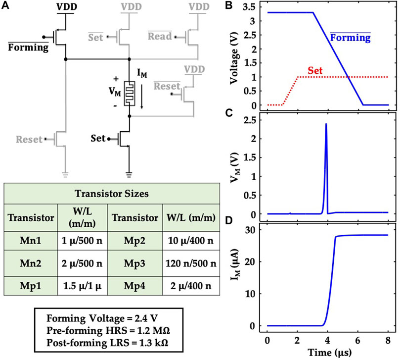
FIGURE 4. (A) Schematic of the memristor-based synapse circuit that can control forming, set, reset and read operations in a memristor device. In this work, the set, reset and readout portions of the circuit are greyed out (unused). (B) Time dynamics of the input signals (
To simulate the forming process in HSPICE, we calibrate the compact model with the relevant parameters (forming voltage, pre-forming HRS, and post-forming LRS), extracted from the KMC + TCAD simulations. Note, the ideal approach to calibrate the compact model would be to use iterations between the circuit level simulations and KMC + TCAD simulations. The approach would include running the KMC + TCAD simulations with the results from the circuit level simulation and then again simulating the circuit with the KMC + TCAD results. But, this would require a compact model that could capture the non-linear behavior observed in the KMC + TCAD simulations. Here, to calibrate the model for circuit simulations, we choose the mean values of the pre-forming HRS (1.2 MΩ), and post-forming LRS (1.3 kΩ) to set up the compact model. As for the forming voltage, we choose the maximum value of the corresponding distribution (2.4 V), to capture the worst-case scenario. For the transistors, we use the DGXFET NMOS/PMOS models for the IBM 65 nm 10LPe process.
Figures 4B–D illustrate the simulated transient characteristics of the synapse circuit (only the forming process), bearing the signature of the circuit-level interactions of the memristor. We govern the forming process with appropriately designed control signals (
3 Results
3.1 Filament Formation Dynamics
Figure 5 shows the filament formation dynamics for a single device simulation at a constant voltage of 3 V applied to the top electrode and 0 V applied to the bottom electrode. For this simulation, the initial defect volume fraction was chosen to correspond with 1 oxygen vacancy within the simulation domain. New defects tend to form in the vicinity of pre-existing defects due to: 1) a lower formation energy in the presence of pre-existing Frenkel pairs; and 2) a higher electric field in the vicinity of a charged filament. As time progresses, filament growth proceeds towards the top electrode, where the electric field is highest. Once the electrodes have bridged, additional filament growth occurs along the width of the top electrode. This occurs due to: 1) a higher lateral electric field, 2) the effect of oxygen gettering by the Ti top electrode, which readily removes oxygen ion interstitials, and 3) screening of the electric field seen by points closer to the bottom electrode by charged vacancies near the top electrode.
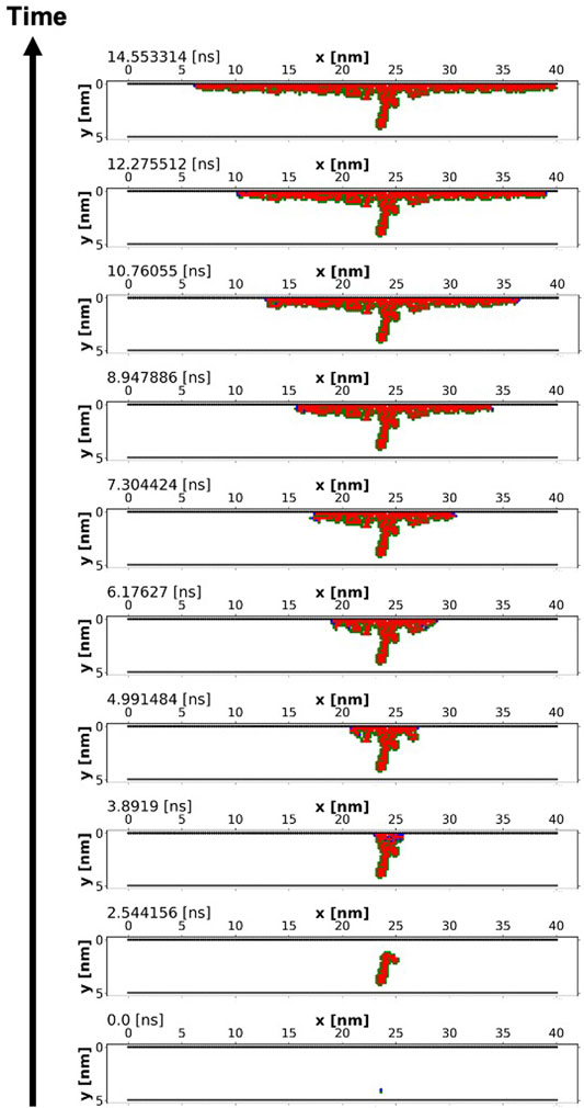
FIGURE 5. An example of filament formation dynamics with the top electrode at 3 V and the bottom electrode at 0 V. The red squares are the filament, the green circles are oxygen ions and the blue circles are unoccupied oxygen vacancies.
Since bond breaking is modeled as a statistical process, it is necessary to evaluate the behavior of more than one device. Thus, we further investigate forming dynamics by assessing the statistical distribution of forming times for repeated device simulations. Here, we focus on the forming time–the time required to form, which we estimate by halting the simulation once a predefined number of filament states are formed. We use a volume fraction of 0.1, which should correspond to a concentration of the order of ≈1 × 1021 cm−3. This is comparable to what has been observed experimentally in HfOx films having high oxygen vacancy concentrations (Hildebrandt et al., 2011), reported as high as 6 × 1021 cm−3.
We note that since the forming process is modeled using the thermochemical model of dielectric breakdown, the forming time is synonymous with the time-dependent-dielectric-breakdown (TDDB), and is therefore an experimental observable which is straightforward to measure and, most importantly, can be used to validate kinetic monte carlo simulation models. Previous authors have compared the effect of top and bottom electrodes on the forming time for nearly stoichiometric 10 nm thick HfO2 thin films deposited by atomic layer deposition (Lorenzi et al., 2013; Cagli et al., 2011). Figure 6 shows a Weibull distribution of forming times obtained from our simulation and those of Lorenzi et al., 2013 for a TiN/HfO2/Pt device at an electric field of 5 MV cm−1 and 6 MV cm−1. Simulation results at both values of electric field show reasonable quantitative agreement to experiment. At the lower electric field of 5 MV cm−1, there appears to be a deviation from a Weibull distribution, however the forming times are similar in magnitude. These results illustrate the similarity between forming time and TDDB, and provide a potential route towards empirical validation of simulation models—from which the activation energy of Frenkel pair generation, Ea,g and the field-acceleration factor, γ can be derived (McPherson and Mogul, 1998).
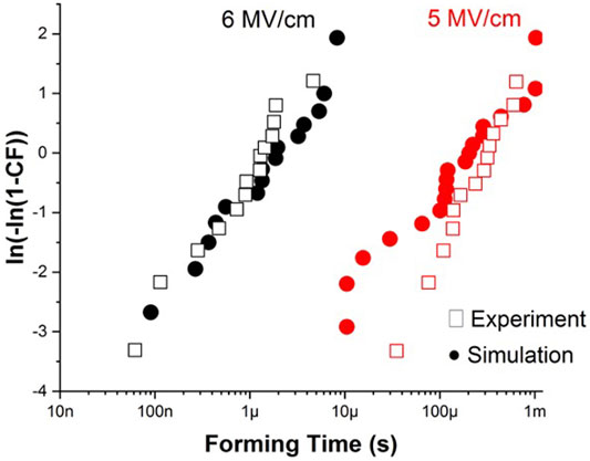
FIGURE 6. Comparison of forming time distributions obtained from our simulations and experimental work (Lorenzi et al., 2013) for a TiN/HfO2/Pt device at an electric field of 5 MV cm−1 and 6 MV cm−1.
This is especially important to establish agreement to experimental results, since HfOx films can exhibit mixed crystalline phases and variable oxygen content depending on deposition conditions—both of which are expected to modify Ea,g and γ.
3.2 Current-Voltage Characteristics
Figure 7 shows the complete current-voltage (IV) characteristics for a forming, reset and set programming cycle. In order to obtain IV characteristics, snapshots of the state of the system are taken at the end of each voltage step shown in Figure 3B. In this case, the time step is 1 µs and the voltage step is 0.1 V. In Figure 7A, intermediate filament states are shown at different stages of programming. It can be seen that, at forming, a large volume fraction of the device consists of oxygen vacancy filament with a structure that extends laterally near the top electrode. The spatial extent of the filament (i.e., volume fraction of vacancies) will ultimately be controlled by the flux linkage (forming voltage × time), which is set by the compliance current in practice.
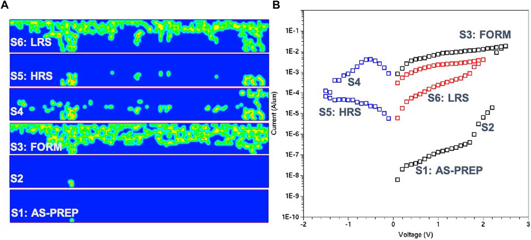
FIGURE 7. (A) Filament positions corresponding to different points along the programming sequence (forming, reset, set). (B) Pulsed IV characteristics for the complete programming sequence.
Several of the well-known aspects of oxide memristors are captured by this simulated result shown in Figure 7B: 1) the high-resistance initial state of the as-prepared thin-film; 2) A low resistance state after forming; 3) A gradual reset behavior with programmable analog high-resistance levels; and 4) A low-resistance state following set of the order of kilo-Ohms. The ability to quantify and visualize the increase in current upon set (potentiation) and the decrease in current upon reset (depression) is a key benefit of Figure 7B incorporating TCAD Sentaurus for modeling synaptic behavior.
3.3 Filament Electrostatics
Figure 8 shows key aspects of the filament electrostatics. In Figure 8A, the electrostatic potential and x and y components of the electric field throughout the device are shown. In regions where the filament bridges the top and bottom electrode, the voltage drop across this region is large enough such that the filament region has a net negative potential near the bottom electrode. This agrees well with experimental results which relied on in-situ TEM electron holography measurements (Li et al., 2017), in which they described the filament as a “negative potential synapse.” Our results show that this stems directly from the negative space-charge associated with the filament, assumed to be due to electron capture (
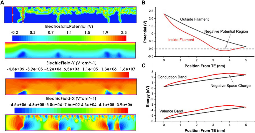
FIGURE 8. (A) Filament electrostatics after forming, including the electrostatic potential, and electric field components. (B) Comparison of electrostatic potential inside and outside of a filament region as indicated in the red lines in (A). The filament region shows a region of negative potential and can be likened to a “negative potential synapse.” (C) Comparison of the energy band diagram inside and outside of the filament. Within the filament, a negative curvature indicates that the filament is a negative space-charge region.
3.4 Monte Carlo Analysis of Synapse Forming Circuit
Finally, we use the unique capability of the KMC + TCAD model to investigate a device-circuit co-design strategy. We test memristor characteristics for different levels of initial oxygen vacancy volume faction (x), a design variable that can be easily controlled during the fabrication process. Figure 9A shows the pre-forming HRS for different values of x for 25 devices (each) obtained from the KMC + TCAD simulations. Considering the circuit-level scenario of a synapse, the variations in the characteristics of multiple transistors need to be superposed with the inherent device-level variations of the memristor. To account for all these variations concurrently, we run 1000-point (3σ) Monte-Carlo simulations for the forming circuit using the data obtained from the KMC + TCAD framework. We utilize the dependence of the pre-forming HRS on the initial oxygen vacancy volume faction and the threshold voltage variation of the PMOS and NMOS transistors to set the input distributions for the Monte-Carlo simulations. Figure 9A shows the pre-forming HRS for different values of x for 25 devices (each) obtained from the KMC + TCAD simulations. Without any loss of generality, we run the Monte-Carlo simulation for two values of x (0.02 and 0.04%). To incorporate the threshold voltage variation of the transistors, we use a gaussian distribution with a mean value equal to the nominal threshold voltage (0.65 V for 65 nm DGXFET transistors) and standard deviation of 20 mV (shown in the table of Figure 9B). We also run the Monte-Carlo simulations with different levels of current compliance, controlled by applying appropriate gate voltage (Set) to Mn1.
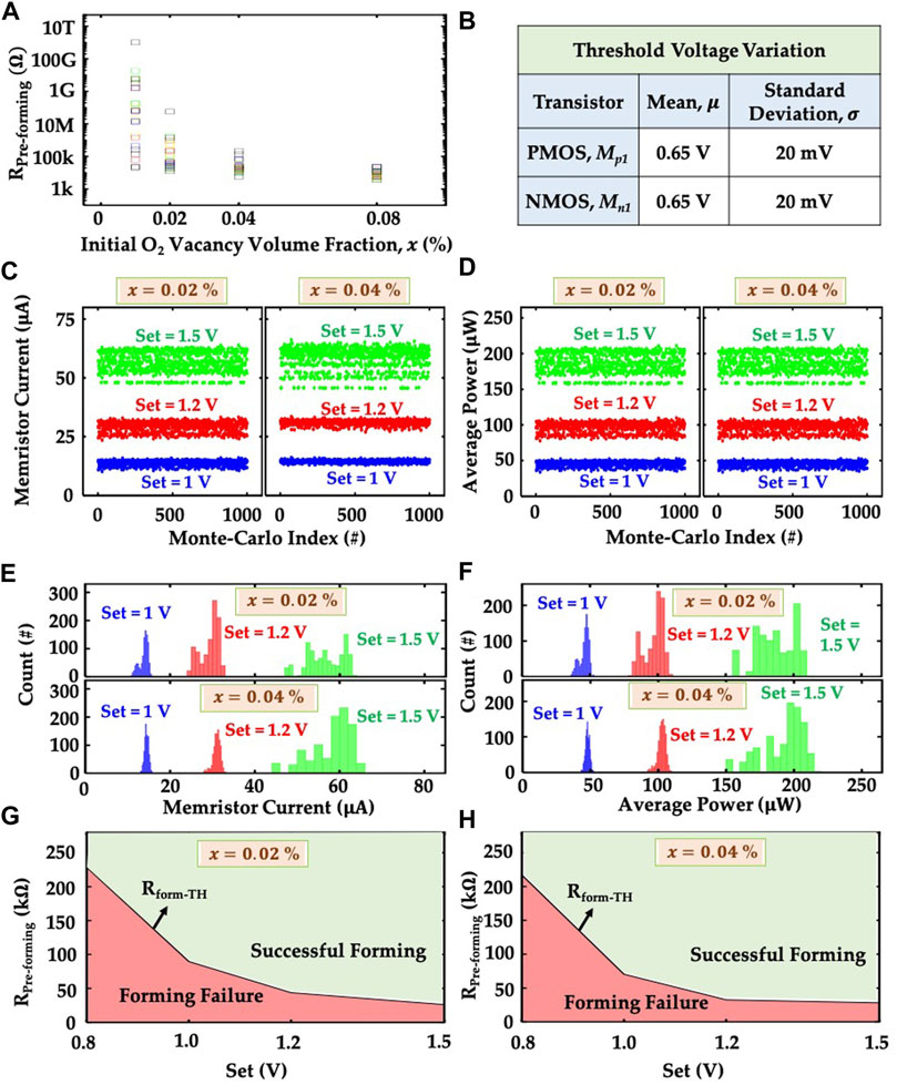
FIGURE 9. (A) Dependence of pre-forming HRS on the initial oxygen vacancy volume fraction (x). These results are obtained from KMC-TCAD simulation for 25 devices. (B) Table shows the values of mean and standard deviation of the threshold voltage distribution of Mp1 and Mn1 transistors used for the Monte-Carlo simulation. Scatter plot of the (C) memristor current, and (D) average power consumption of the forming circuit obtained from the 1,000 point Monte-Carlo simulation for three different values of Set (1 V, 1.2 and 1.5 V) and the pre-forming HRS values for two different values of x (0.02 and 0.04%). Histogram plot of the (E) memristor current, and (F) average power consumption of the forming circuit for the data shown in the scatter plots of (C) and (D) respectively. Dependence of forming success and failure on the values of Set for the pre-forming HRS values obtained for (g) x = 0.02%, and (h) x = 0.04%.
Figures 9C,D show the scatter plots for the average current through the memristor and average power of the forming circuit, respectively. Each of these metrics have been reported for different levels of compliance currents (different levels of Set). To ensure a fair comparison, we allow a constant time for the forming process for all cases. Naturally, we observe that for lower compliance limits, many instances of the Monte-Carlo simulations exhibit “unsuccessful” forming. Note, a compliance limit may lead to a different level of post-forming LRS and hence might be treated as successful, if the post-forming LRS is known during the design stage. However, if such changes in the post-forming LRS occurs dynamically and randomly, those will lead to read/sense failure. Therefore, we simplify our analysis by tagging such cases as ‘Forming Failure’. Higher compliance limit allows most memristor instances to successfully form and hence leads to a larger average current level (Figure 9C). If the memristor can successfully form, it goes to post-forming LRS (1.3kω in our simulation). Otherwise, it remains in the pre-forming HRS which is much larger compared to LRS. Therefore, the increase in the value of Set increases the average current of the memristor due to the increase in the number of formed memristors. Since, the average power of the forming circuit is very closely related to the memristor current, the average forming power shows the same trend like the average memristor current (Figure 9D). The initial oxygen vacancy volume factions lead to similar results, with different levels of mean value and standard deviation for the memristor current and forming power (Figures 9C,D). Figure 9A shows that the pre-forming HRS for x = 0.02% has a larger standard deviation compared to that for x = 0.04%. Therefore, the memristor current and forming power obtained from the Monte-Carlo simulation show larger standard deviation for x = 0.02% compared to the case of x = 0.04%. But only for Set = 1.5 V, the smallest value of pre-forming HRS of the memristors that cannot form becomes comparable to the value of the post-forming LRS. Therefore, the effect of x on the standard deviation of the memristor current and forming power gets suppressed. Figures 9E,F show the histogram plot for Monte-Carlo results of memristor current and forming power shown in the scatter plots (Figures 9C,D).
Based on these Monte-Carlo simulations, we correlate the compliance limits (controlled by the Set pulse) with the pre-forming HRS (RPre−forming) level of the memristor. Figure 9G illustrates the combinations of Set and RPre−forming that lead to successful forming (and vice versa). Clearly, for a given compliance limit, the pre-forming HRS level of a memristor needs to be higher than a critical threshold (Rform−TH), illustrated (in Figure 9G) as a line separating the successful and unsuccessful forming cases. Figure 9H shows similar trends for a different initial oxygen vacancy volume faction. Our analysis shows a pathway to optimize the synapse circuit by correlating the material and circuit-level design knobs.
4 Conclusion
The ability to design and implement fast, scalable and robust neuromorphic systems relies heavily upon our fundamental understanding of memristor switching. Oxide memristors, envisioned for RRAM-based neuromorphic systems, exhibit changes in resistance state through multiple synergistic effects involving electronic and atomic degrees of freedom, often modelled as separate influences. One of the main purposes of this work was to establish a more direct connection between the two in order to: 1) provide a unified view of filament evolution and electronic conduction; 2) to implement this description within a state-of-the-art TCAD framework for modeling electric conduction; and 3) gain circuit-level insight.
Here, we have argued the use of a simple model of filament evolution that makes explicit use of Fermi-Dirac statistics, coupling the rate of defect generation and recombination to electronic transitions associated with conduction and lattice relaxation. By combining Synopsys TCAD Sentaurus with Kinetic Monte Carlo simulations of filament evolution, we have shown the ability to quantify both the common and subtle aspects of resistive-switching behavior of HfOx memristors. Quasi-static snapshots of the device state—consisting of positive/negative oxygen vacancies, and oxygen ions—were taken at various voltages to obtain IV characteristics under stepped voltage ramp conditions. Electric conduction in oxygen vacancy filaments is modeled as trap-to-band transitions between occupied and unoccupied electronic states assisted by multiphonon absorption and emission. According to Fermi-Dirac statistics, such processes are expected to occur within a band of energies in the vicinity of the Fermi level wherein both occupied and unoccupied states are probable. Thus, the occupancy of a trap and its relation to the Fermi level is fundamentally related to transition rates associated with electronic conduction. The use of TCAD Sentaurus provides a powerful framework for modeling these and other conduction processes as well as visualizing filament electrostatics, as we’ve shown. In particular, we have obtained results that are consistent with experimental observations of a negative space charge and potential associated with a vacancy-rich filament. Our approach will enable the more efficient evaluation of memristor device behavior and circuit performance, stemming from physics-based modeling, having a direct impact and benefit on the fields of neuromorphic computing, memory design and dynamical systems.
Data Availability Statement
The raw data supporting the conclusion of this article will be made available by the authors, without undue reservation.
Author Contributions
AZ conceived of and designed the Kinetic Monte Carlo algorithm and TCAD Sentaurus modeling framework. SA performed the transient simulations, and the circuit-level Monte Carlo analysis. ZW assisted with device-level simulations and parameter influences. RW designed the synapse circuit. AA analyzed the circuit simulations and Monte Carlo data. AZ AA, and GR jointly supervised the work and analyzed the results. All authors contributed to writing the article and approving the submitted version.
Funding
This material is based in part on research sponsored by Air Force Research Laboratory under agreement number FA8750-19-1-0025. The U.S. Government is authorized to reproduce and distribute reprints for Governmental purposes notwithstanding any copyright notation thereon. The views and conclusions contained herein are those of the authors and should not be interpreted as necessarily representing the official policies or endorsements, either expressed or implied, of Air Force Research Laboratory or the U.S. Government.
Conflict of Interest
The authors declare that the research was conducted in the absence of any commercial or financial relationships that could be construed as a potential conflict of interest.
Publisher’s Note
All claims expressed in this article are solely those of the authors and do not necessarily represent those of their affiliated organizations, or those of the publisher, the editors and the reviewers. Any product that may be evaluated in this article, or claim that may be made by its manufacturer, is not guaranteed or endorsed by the publisher.
Acknowledgments
The authors would like to acknowledge helpful conversations with Dr. Nathaniel Cady of SUNY Polytechnic Institute at Albany, NY.
Supplementary Material
The Supplementary Material for this article can be found online at: https://www.frontiersin.org/articles/10.3389/fnano.2021.734121/full#supplementary-material
References
Aldana, S., Garcia-Fernandez, P., Romero-Zaliz, R., Gonzalez, M. B., Jimenez-Molinos, F., Campabadal, F., et al. (2018). “A Kinetic Monte Carlo Simulator to Characterize Resistive Switching and Charge Conduction in Ni/HfO2/Si RRAMs,” in Proceedings Of The 2018 12th Spanish Conference On Electron Devices (Cde). Editors J. Mateos, and T. Gonzalez (NEW YORK, NY 10017 USA: IEEESpanish Conference on Electron DevicesBackup Publisher: IEEE; Univ Salamanca ISSN), 2163–4971. Type: Proceedings Paper.
Aldana, S., Garcia-Fernandez, P., Romero-Zaliz, R., Gonzalez, M. B., Jimenez-Molinos, F., Gomez-Campos, F., et al. (2020). Resistive Switching in HfO2 Based Valence Change Memories, a Comprehensive 3D Kinetic Monte Carlo Approach. JOURNAL PHYSICS D-APPLIED PHYSICS 53. doi:10.1088/1361-6463/ab7bb6
Amer, S., Hasan, M. S., and Rose, G. S. (2017a). Analysis and Modeling of Electroforming in Transition Metal Oxide-Based Memristors and its Impact on Crossbar Array Density. IEEE Electron. Device Lett. 39, 19–22.
Amer, S., Rose, G. S., Beckmann, K., and Cady, N. C. (2017b). Design Techniques for In-Field Memristor Forming Circuits. In 2017 IEEE 60th International Midwest Symposium on Circuits and Systems (MWSCAS). IEEE, 1224–1227. doi:10.1109/mwscas.2017.8053150
Amer, S., Sayyaparaju, S., Rose, G. S., Beckmann, K., and Cady, N. C. (2017c). A Practical Hafnium-Oxide Memristor Model Suitable for Circuit Design and Simulation. In 2017 IEEE International Symposium on Circuits and Systems (ISCAS), 1–IEEE4. doi:10.1109/iscas.2017.8050790
Beckmann, K., Holt, J., Manem, H., Van Nostrand, J., and Cady, N. C. (2016). Nanoscale Hafnium Oxide Rram Devices Exhibit Pulse Dependent Behavior and Multi-Level Resistance Capability. Mrs Adv. 1, 3355–3360. doi:10.1557/adv.2016.377
Bianchi, S., Pedretti, G., Munoz-Martin, I., Calderoni, A., Ramaswamy, N., Ambrogio, S., et al. (2020). A Compact Model for Stochastic Spike-timing-dependent Plasticity (STDP) Based on Resistive Switching Memory (RRAM) Synapses. IEEE Trans. Electron. Devices 67, 2800–2806. doi:10.1109/TED.2020.2992386
Bradley, S. R., Shluger, A. L., and Bersuker, G. (2015). Electron-Injection-Assisted Generation of Oxygen Vacancies in MonoclinicHfO2. Phys. Rev. Appl. 4, 064008. doi:10.1103/PhysRevApplied.4.064008
Cagli, C., Buckley, J., Jousseaume, V., Cabout, T., Salaun, A., Grampeix, H., et al. (2011). Experimental and Theoretical Study of Electrode Effects in HfO2 Based RRAM. In 2011 International Electron Devices Meeting. 28. 7.1–28.7.4. doi:10.1109/IEDM.2011.6131634.ISSN:2156-017X
Chen, A. (2013). Area and Thickness Scaling of Forming Voltage of Resistive Switching Memories. IEEE Electron. Device Letters 35, 57–59.
Choi, B. J., Torrezan, A. C., Strachan, J. P., Kotula, P. G., Lohn, A. J., Marinella, M. J., et al. (2016). High‐Speed and Low‐Energy Nitride Memristors. Adv. Funct. Mater. 26, 5290–5296. doi:10.1002/adfm.201600680
Chua, L. (1971). Memristor-the Missing Circuit Element. IEEE Trans. Circuit Theor. 18, 507–519. doi:10.1109/tct.1971.1083337
Englman, R., and Jortner, J. (1970). The Energy gap Law for Radiationless Transitions in Large Molecules. Mol. Phys. 18, 145–164. doi:10.1080/00268977000100171
Fichthorn, K. A., and Weinberg, W. H. (1991). Theoretical Foundations of Dynamical Monte Carlo Simulations. J. Chem. Phys. 95, 1090–1096. doi:10.1063/1.461138
Govoreanu, B., Kar, G., Chen, Y., Paraschiv, V., Kubicek, S., Fantini, A., et al. (2011). 10× 10nm 2 Hf/hfo X Crossbar Resistive Ram with Excellent Performance, Reliability and Low-Energy Operation. In 2011 International Electron Devices Meeting. IEEE, 31–36.
Guan, X., Yu, S., and Wong, H.-S. P. (2012b). A Spice Compact Model Of Metal Oxide Resistive Switching Memory With Variations. IEEE Electron. Device Lett. 33, 1405–1407. doi:10.1109/LED.2012.2210856
Guan, X., Yu, S., and Wong, H.-S. P. (2012a). On the Switching Parameter Variation of Metal-Oxide RRAM-Part I: Physical Modeling and Simulation Methodology. IEEE Trans. Electron. Devices 59, 1172–1182. doi:10.1109/TED.2012.2184545
Hazra, J., Liehr, M., Beckmann, K., Rafiq, S., and Cady, N. (2020). Impact of Atomic Layer Deposition Co-reactant Pulse Time on 65nm CMOS Integrated Hafnium Dioxide-Based Nanoscale RRAM Devices. In 2020 IEEE International Integrated Reliability Workshop (IIRW). South Lake Tahoe, CA, USA: IEEE, 1–4. doi:10.1109/IIRW49815.2020.9312877
Hazra, J., Liehr, M., Beckmann, K., Rafiq, S., and Cady, N. (2019). Improving the Memory Window/Resistance Variability Trade-Off for 65nm CMOS Integrated HfO2 Based Nanoscale RRAM Devices. In 2019 IEEE International Integrated Reliability Workshop (IIRW). South Lake Tahoe, CA, USA: IEEE, 1–4. doi:10.1109/IIRW47491.2019.8989872
Henry, C. H., and Lang, D. V. (1977). Nonradiative Capture and Recombination by Multiphonon Emission in GaAs and GaP. Phys. Rev. B 15, 989–1016. doi:10.1103/PhysRevB.15.989
Hildebrandt, E., Kurian, J., Müller, M. M., Schroeder, T., Kleebe, H.-J., and Alff, L. (2011). Controlled Oxygen Vacancy Induced P-type Conductivity in HfO2−x Thin Films. Appl. Phys. Lett. 99, 112902. doi:10.1063/1.3637603
Ho, M.-Y., Gong, H., Wilk, G. D., Busch, B. W., Green, M. L., Voyles, P. M., et al. (2003). Morphology and Crystallization Kinetics in HfO2 Thin Films Grown by Atomic Layer Deposition. J. Appl. Phys., 93, 1477–1481. doi:10.1063/1.1534381
Hu, M., Strachan, J. P., Li, Z., and Stanley, R. (2016). Dot-product Engine as Computing Memory to Accelerate Machine Learning Algorithms. In 2016 17th International Symposium on Quality Electronic Design (ISQED). IEEE, 374–379. doi:10.1109/isqed.2016.7479230
Huang, P., Deng, Y., Gao, B., Chen, B., Zhang, F., Yu, D., et al. (2013a). Optimization of Conductive Filament of Oxide-Based Resistive-Switching Random Access Memory for Low Operation Current by Stochastic Simulation. Jpn. J. Appl. Phys. 52, 04CD04. doi:10.7567/JJAP.52.04CD04
Huang, P., Liu, X. Y., Chen, B., Li, H. T., Wang, Y. J., Deng, Y. X., et al. (2013b). A Physics-Based Compact Model of Metal-Oxide-Based RRAM DC and AC Operations. IEEE Trans. Electron. Devices 60, 4090–4097. doi:10.1109/ted.2013.2287755
Jansen, A. P. J. (2012). An Introduction to Kinetic Monte Carlo Simulations of Surface Reactions, 856. Springer.
Jiang, Z., Yu, S., Wu, Y., Engel, J. H., Guan, X., and Wong, H.-S. P. (2014). Verilog-A Compact Model for Oxide-Based Resistive Random Access Memory (RRAM). In 2014 International Conference on Simulation of Semiconductor Processes and Devices (SISPAD). Yokohama, Japan: IEEE, 41–44. doi:10.1109/SISPAD.2014.6931558
Jiménez-Molinos, F., Gámiz, F., Palma, A., Cartujo, P., and López-Villanueva, J. A. (2002). Direct and Trap-Assisted Elastic Tunneling through Ultrathin Gate Oxides. J. Appl. Phys. 91, 5116–5124. doi:10.1063/1.1461062
Kim, W., Wouters, D. J., Menzel, S., Rodenbücher, C., Waser, R., and Rana, V. (2016). Lowering Forming Voltage and Forming-free Behavior of Ta 2 O 5 Reram Devices. In 2016 46th European Solid-State Device Research Conference (ESSDERC). IEEE, 164–167.
Koveshnikov, S., Matthews, K., Min, K., Gilmer, D., Sung, M., Deora, S., et al. (2012). Real-time Study of Switching Kinetics in Integrated 1t/hfo X 1r Rram: Intrinsic Tunability of Set/reset Voltage and Trade-Off with Switching Time. In 2012 International Electron Devices Meeting. IEEE, 20–24.
Kumar, S., Wang, Z., Huang, X., Kumari, N., Davila, N., Strachan, J. P., et al. (2017). Oxygen Migration during Resistance Switching and Failure of Hafnium Oxide Memristors. Appl. Phys. Lett. 110, 103503. doi:10.1063/1.4974535
Larcher, L., Padovani, A., Pirrotta, O., Vandelli, L., and Bersuker, G. (2012). Microscopic Understanding and Modeling of HfO2 RRAM Device Physics. In 2012 International Electron Devices Meeting. 20. 1.1–20.1.4. doi:10.1109/IEDM.2012.6479077.ISSN:2156-017X
Li, C., Belkin, D., Li, Y., Yan, P., Hu, M., Ge, N., et al. (2018a). Efficient and Self-Adaptive In-Situ Learning in Multilayer Memristor Neural Networks. Nat. Commun. 9, 2385–2388. doi:10.1038/s41467-018-04484-2
Li, C., Gao, B., Yao, Y., Guan, X., Shen, X., Wang, Y., et al. (2017). Direct Observations of Nanofilament Evolution in Switching Processes in HfO2-Based Resistive Random Access Memory by In Situ TEM Studies. Adv. Mater. 29, 1602976. doi:10.1002/adma.201602976
Li, C., Hu, M., Li, Y., Jiang, H., Ge, N., Montgomery, E., et al. (2018b). Analogue Signal and Image Processing with Large Memristor Crossbars. Nat. Electron. 1, 52–59. doi:10.1038/s41928-017-0002-z
Lima, L. P. B., Diniz, J. A., Doi, I., and Godoy Fo, J. (2012). Titanium Nitride as Electrode for MOS Technology and Schottky Diode: Alternative Extraction Method of Titanium Nitride Work Function. Microelectronic Eng. 92, 86–90. doi:10.1016/j.mee.2011.04.059
Liu, H., Lv, H., Yang, B., Xu, X., Liu, R., Liu, Q., et al. (2014). Uniformity Improvement in 1t1r Rram with Gate Voltage Ramp Programming. IEEE Electron. Device Lett. 35, 1224–1226. doi:10.1109/led.2014.2364171
Lorenzi, P., Rao, R., and Irrera, F. (2013). Forming Kinetics in $\hbox{HfO}_{2}$ -Based RRAM Cells. IEEE Trans. Electron. Devices 60, 438–443. doi:10.1109/TED.2012.2227324
Loy, D. J. J., Dananjaya, P. A., Chakrabarti, S., Tan, K. H., Chow, S. C. W., Toh, E. H., et al. (2020). Oxygen Vacancy Density Dependence with a Hopping Conduction Mechanism in Multilevel Switching Behavior of HfO2-Based Resistive Random Access Memory Devices. ACS Appl. Electron. Mater. 2, 3160–3170. Place: 1155 16TH ST, NW, WASHINGTON, DC 20036 USA Publisher: AMER CHEMICAL SOC Type: Article. doi:10.1021/acsaelm.0c00515
Manem, H., Rajendran, J., and Rose, G. S. (2012). Design Considerations for Multilevel CMOS/Nano Memristive Memory. J. Emerg. Technol. Comput. Syst. 8, 1–22. doi:10.1145/2093145.2093151
McPherson, J., Kim, J.-Y., Shanware, A., and Mogul, H. (2003). Thermochemical Description of Dielectric Breakdown in High Dielectric Constant Materials. Appl. Phys. Lett. 82, 2121–2123. doi:10.1063/1.1565180
McPherson, J. W., and Mogul, H. C. (1998). Underlying Physics of the Thermochemical E Model in Describing Low-Field Time-dependent Dielectric Breakdown in SiO2 Thin Films. J. Appl. Phys. 84, 1513–1523. doi:10.1063/1.368217
Nasyrov, K. A., and Gritsenko, V. A. (2011). Charge Transport in Dielectrics via Tunneling between Traps. J. Appl. Phys. 109, 093705. doi:10.1063/1.3587452
Nasyrov, K. A., Gritsenko, V. A., Novikov, Y. N., Lee, E.-H., Yoon, S. Y., and Kim, C. W. (2004). Two-bands Charge Transport in Silicon Nitride Due to Phonon-Assisted Trap Ionization. J. Appl. Phys. 96, 4293–4296. doi:10.1063/1.1790059
Palma, A., Godoy, A., Jiménez-Tejada, J. A., Carceller, J. E., and López-Villanueva, J. A. (1997). Quantum Two-Dimensional Calculation of Time Constants of Random Telegraph Signals in Metal-Oxide-Semiconductor Structures. Phys. Rev. B 56, 9565–9574. doi:10.1103/PhysRevB.56.9565
Pi, S., Li, C., Jiang, H., Xia, W., Xin, H., Yang, J. J., et al. (2019). Memristor Crossbar Arrays with 6-nm Half-Pitch and 2-nm Critical Dimension. Nat. Nanotech 14, 35–39. doi:10.1038/s41565-018-0302-0
Raghavan, N., Frey, D. D., Bosman, M., and Pey, K. L. (2015). Statistics of Retention Failure in the Low Resistance State for Hafnium Oxide RRAM Using a Kinetic Monte Carlo Approach. Microelectronics Reliability 55, 1422–1426. doi:10.1016/j.microrel.2015.06.090
Schenk, A., and Heiser, G. (1997). Modeling and Simulation of Tunneling through Ultra-thin Gate Dielectrics. J. Appl. Phys. 81, 7900–7908. doi:10.1063/1.365364
Sementa, L., Larcher, L., Barcaro, G., and Montorsi, M. (2017). Ab Initio modelling of Oxygen Vacancy Arrangement in Highly Defective HfO2 Resistive Layers. Phys. Chem. Chem. Phys. 19, 11318–11325. doi:10.1039/C7CP01216K
Sire, C., Blonkowski, S., Gordon, M. J., and Baron, T. (2007). Statistics of Electrical Breakdown Field in HfO2 and SiO2 Films from Millimeter to Nanometer Length Scales. Appl. Phys. Lett. 91, 242905. doi:10.1063/1.2822420
Stout, V. L., and Gibbons, M. D. (1955). Gettering of Gas by Titanium. J. Appl. Phys. 26, 1488–1492. doi:10.1063/1.1721936
Strukov, D. B., Snider, G. S., Stewart, D. R., and Williams, R. S. (2008). The Missing Memristor Found. nature 453, 80–83. doi:10.1038/nature06932
Xia, Q., and Yang, J. J. (2019). Memristive Crossbar Arrays for Brain-Inspired Computing. Nat. Mater. 18, 309–323. doi:10.1038/s41563-019-0291-x
Xu, X., Rajendran, B., and Anantram, M. P. (2020). Kinetic Monte Carlo Simulation of Interface-Controlled Hafnia-Based Resistive Memory. IEEE Trans. Electron. Devices 67, 118–124. doi:10.1109/TED.2019.2953917
Yao, P., Wu, H., Gao, B., Eryilmaz, S. B., Huang, X., Zhang, W., et al. (2017). Face Classification Using Electronic Synapses. Nat. Commun. 8, 1–8. doi:10.1038/ncomms15199
Yao, P., Wu, H., Gao, B., Zhang, G., and Qian, H. (2015). The Effect of Variation on Neuromorphic Network Based on 1t1r Memristor Array. In 2015 15th Non-Volatile Memory Technology Symposium (NVMTS). IEEE, 1–3. doi:10.1109/nvmts.2015.7457492
Keywords: memristor, neuromorphic, nanoelectronics, non-volatile memory, RRAM, Monte Carlo, TCAD Sentaurus
Citation: Zeumault A, Alam S, Wood Z, Weiss RJ, Aziz A and Rose GS (2021) TCAD Modeling of Resistive-Switching of HfO2 Memristors: Efficient Device-Circuit Co-Design for Neuromorphic Systems. Front. Nanotechnol. 3:734121. doi: 10.3389/fnano.2021.734121
Received: 30 June 2021; Accepted: 20 September 2021;
Published: 06 October 2021.
Edited by:
Huanglong Li, Tsinghua University, ChinaCopyright © 2021 Zeumault , Alam , Wood , Weiss , Aziz and Rose . This is an open-access article distributed under the terms of the Creative Commons Attribution License (CC BY). The use, distribution or reproduction in other forums is permitted, provided the original author(s) and the copyright owner(s) are credited and that the original publication in this journal is cited, in accordance with accepted academic practice. No use, distribution or reproduction is permitted which does not comply with these terms.
*Correspondence: Andre Zeumault , YXpldW1hdWx0QHV0ay5lZHU=