 Larionette P. L. Mawlong1†
 Ravi K. Biroju
- 1Center for Nanotechnology, Indian Institute of Technology Guwahati, Guwahati, India
- 2Department of Basic Science and Humanities, Koneru Lakshmaiah Education Foundation, Hyderabad, India
- 3Department of Physics, Indian Institute of Technology Guwahati, Guwahati, India
We report on the growth of an ordered array of MoS2 nanodots (lateral sizes in the range of ∼100–250 nm) by a thermal chemical vapor deposition (CVD) method directly onto SiO2 substrates at a relatively low substrate temperature (510–560°C). The temperature-dependent growth and evolution of MoS2 nanodots and the local environment of sulfur-induced structural defects and impurities were systematically investigated by field emission scanning electron microscopy, micro-Raman spectroscopy, and X-ray photoelectron spectroscopy (XPS) techniques. At the substrate temperature of 560°C, we observed mostly few-layer MoS2, and at 510°C, multilayer MoS2 growth, as confirmed from the Raman line shape analysis. With reduced substrate temperature, the density of MoS2 nanodots decreases, and layer thickness increases. Raman studies show characteristic Raman modes of the crystalline MoS2 layer, along with two new Raman modes centered at ∼346 and ∼361 cm−1, which are associated with MoO2 and MoO3 phases, respectively. Room temperature photoluminescence (PL) studies revealed strong visible PL from MoS2 layers, which is strongly blue-shifted from the bulk MoS2 flakes. The strong visible emission centered at ∼ 658 nm signifies a free excitonic transition in the direct gap of single-layer MoS2. Position-dependent PL profiles show excellent uniformity of the MoS2 layers for samples grown at 540 and 560°C. These results are significant for the low-temperature CVD growth of a few-layer MoS2 dots with direct bandgap photoluminescence on a flexible substrate.
Introduction
Since the discovery of graphene, two-dimensional materials have attracted much interest due to their interesting optical, electrical, and mechanical characteristics. Molybdenum disulfide (MoS2), a transition metal dichalcogenide (TMD), has a layered structure of hexagonally arranged covalently bonded Mo and S atoms. The vast difference in the electronic structure of the bulk in comparison with the monolayer MoS2 offers a great opportunity for diverse applications. It has an excellent on/off ratio of 108 (Radisavljevic et al., 2011) and a high carrier mobility up to 200 cm2/ Vs at room temperature (Radisavljevic et al., 2011), making it a promising candidate for optoelectronic applications, such as photodetectors (Yin et al., 2012), (Lee et al., 2012)photovoltaics, (Feng et al., 2012; Bernardi et al., 2013; Fontana et al., 2013), light emitters (Ye et al., 2014), and photo (electro)catalysis. (Biroju et al., 2017a; Biroju et al., 2017b). Its high mechanical strength and flexibility open up new scope for future electronic and optoelectronic applications. Different methods, such as hydrothermal synthesis (Rao and Nag, 2010), different types of exfoliation (Zeng et al., 2011; Zhou et al., 2011; Li et al., 2012a), and physical vapor deposition (Gong et al., 2013; Muratore et al., 2014) techniques, have been used for the growth of MoS2. However, the lateral size of MoS2 domains synthesized by these methods is often restricted to several micrometers, making the synthesis of a large-area MoS2 thin layer challenging. Among the different methods, chemical vapor deposition (CVD) has been one of the most promising methods of producing large-area and high-quality MoS2 thin films (Zhang et al., 2014; Jeon et al., 2015; Liu et al., 2015; Yu et al., 2015).
However, a certain amount of defects and impurities is usually present in single-crystalline nanomaterials and even with small imperfections. Particularly, in the case of CVD-grown graphene and related 2D-layered semiconductors, plenty of in-plane point defects and extended defects are often introduced during the CVD growth process. These defects play an important role in tuning the electrical and optical properties of MoS2. The change in the nature of bandgap in MoS2 from indirect to direct type, as the layer number is thinned down to a monolayer (Mak et al., 2010), leads to an extraordinary visible photoluminescence (PL) and a robust visible light response in monolayer MoS2. However, quite often, the CVD-grown monolayer and few-layer MoS2 have lagged behind the expectation for a high-quality direct bandgap semiconductor, mainly because of the intrinsic defects such as sulfur-induced vacancies and Mo- and S-induced complex/ligand impurities and heavy intrinsic n-type doping in monolayer MoS2 (Mak et al., 2013). Further, the CVD growth of the MoS2 layer at a relatively low temperature compatible with the microelectronic industry is quite challenging, including the question as to how this study improves the existing knowledge in this area about the MoS2 dots and quantum dots.
Here, we demonstrate the CVD growth of highly crystalline MoS2 dots on SiO2 at a relatively low growth temperature (510–560°C). CVD growth of TMDs on various substrates such as SiO2, quartz, and sapphire is usually carried out at high temperatures ranging from 650 to 850°C using atmospheric CVD to grow single crystals or low-pressure CVD to grow films. (Zhang, 2015; Ganatra and Zhang, 2014; Lee et al., 2320). Note that there are very few reports on the direct CVD growth of TMDs on various kinds of substrates. (Mun et al., 2016a; Gong et al., 2017). For flexible and stretchable devices, MoS2 is one of the suitable materials among the TMDs. Flexible substrates usually have a low melting temperature. So direct growth on these substrates poses a considerable challenge; usually, the MoS2 grown at high temperature is transferred onto these substrates to fabricate the devices. When a comparison is made between the transfer and the direct growth method, the former method may have some structure deformation which may create some defects that may affect its semiconducting properties. Thus, a low-temperature direct growth method is always preferable for the fabrication of nanoelectronic devices (Mun et al., 2016b). We have investigated the sulfur (S)-induced surface defects on as-grown MoS2 dots using position-dependent micro-Raman spectroscopy and X-ray photoelectron spectroscopy (XPS) analyses. Some new Raman bands at 346 and 365 cm−1 were identified, besides the characteristic Raman signatures of MoS2 (E2g and A1g), which are associated with the presence of MoO2 and MoO3. The Raman features of the as-grown MoS2 dots were fully consistent with the XPS analysis. The XPS spectral line shape analysis of Mo-3d and S-2p core level peaks reveals a high amount of S vacancies in the as-grown MoS2 dots.
Experimental
Few layered MoS2 dots were directly grown on the SiO2 substrates using an in-house developed CVD system. Commercially procured MoO3 and S powder were used as precursors for the CVD growth of MoS2 in a quartz tube–based horizontal muffle furnace. High-purity argon (Ar) gas was used as the carrier gas. At first, the S precursor was kept near the entrance of the quartz tube, away from the central heating zone of the furnace, while the MoO3 powder was placed at the center of the furnace, and a few pieces of bare SiO2 substrates were placed near the source powder at the rear end side of the quartz tube. Note that both S and MoO3 precursors were separately loaded in two mini quartz tubes (inner diameter∼10 mm) and kept at a distance of 53 and 33 cm away from the substrates (see Supplementary Figure S1). This arrangement provides stable evaporation of S and MoO3 sources at suitable temperatures and avoids any cross-contaminations during the MoS2 growth. The quartz chamber was pumped down to a base pressure of 1.9 × 10⁻² mbar, and the central zone temperature was raised to 760°C at the rate of 17°C/ min for 45 min and was allowed to stabilize at this temperature for 15 min with Ar as the carrier gas with a flow rate of 100 sccm (standard cubic centimeters per minute), keeping the pressure at 2.2 mbar. Then, it was ramped up slowly to 800°C at the rate of 4°C/ min and then, maintained at this temperature for 30 min without changing the gas flow. After the growth process, the system was allowed to cool down to room temperature with an Ar gas flow of 300 sccm. The experimental setup and the complete timeline profile of the CVD-grown MoS2 dots are shown in Supplementary Figure S1. The substrate temperature is controlled by the proper positioning of the substrate inside the furnace. The temperature at each position corresponding to the substrate was calibrated using an external thermocouple prior to the growth of MoS2 nanodots. The MoS2 growth was monitored at four different substrate temperatures. The samples grown at substrate temperatures of 560, 540, 510, and 310°C are named as MS-560, MS-540, MS-510, and MS-310, respectively.
Characterization
Micro-Raman and PL measurements were performed with a high-resolution spectrometer (Horiba 171 LabRam HR), with excitation wavelengths (λex) of 488 and 514.5 nm (Ar+ ion laser). The excitation source was focused with a 100× objective lens, a spot size of 2 μm, and a laser power of 1.5 mW, and the signal was collected by a CCD in a back scattering geometry sent through a multimode fiber grating of 1800 grooves/ mm. X-ray photoelectron spectroscopy (XPS) measurements were performed with a fully automated XPS microprobe (PHI-Xtool, Ulvac-Phi) using an Al Kα X-ray beam (1486.7 186 eV). The standard carbon 1s spectrum was used to calibrate the XPS spectra recorded for various samples with the spectral resolution of 0.2 eV. Surface morphology and microstructure of the MoS2 dots were examined by using a field emission scanning electron microscope (FESEM), FEI-Quanta 400 with an acceleration voltage of 20 kV with spatial resolution: 1.2 nm at 30 kV in SE, 2 nm at 30 kV in BSE (gold/carbon), detectors: SE, BSE. Spectral line shapes of the micro-Raman features were fitted by Lorentzian line shapes. The XPS line shape profile for all the samples was performed by Shirley peak fitting using Peakfit software with peak parameters as free variables. The best fit was obtained by a large number of iterations.
Results and Discussions
FESEM Studies
In order to understand the morphology of the as-grown samples, FESEM imaging was carried out. A detailed description of the sample growth conditions and FESEM features is provided in Supplementary Table S1. Figures 1A,B show the FESEM images of sample MS-560 at two different magnifications, while Figures 1C,D represent the FESEM images of sample MS-510. It is clear that in each sample, MoS2 dots of a variety of sizes are formed. The uniformity of these dots is almost maintained throughout the surface of the sample, estimated as 1 cm × 1 cm. We observed that the MS-560 has a doughnut-shaped structure of MoS2 dots, which are denser and smaller than that of MS-510. The shape of the MS-510 dots is mostly circular, and a regular array type structure is formed. The observed regular array of MoS2 dots is likely to be due to the direction of the outgoing carrier gas flow.
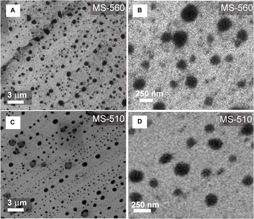
FIGURE 1. Morphological characteristics of MoS2 dots grown by a CVD method: Low- and high-resolution FESEM images of as-grown MoS2 dots in (A–B) MS-560, (C–D) MS-510.
AFM Studies
Figures 2A,B show the AFM images of the as-grown samples grown at different substrate temperatures. For the same growth duration, but at different growth temperatures, we notice an evolution of the morphology of the MoS2 nanodots. In the experiment, we observed that as the substrate is at higher temperature and close to the center of the quartz tube, higher density of the MoS2 nanodots are formed and the corresponding sizes are smaller. In Figures 2A,B for the MS-560 sample, the MoS2 nanodots show some kind of a ring-like structure. These rings are evenly distributed throughout the sample. The average size is estimated to be ∼200 nm. We can also see from the AFM height profile (Figure 2C) that bilayer and a few-layer MoS2 were grown at this temperature (560°C). In Figures 2D,E, for the MS-540 sample, we notice that the MoS2 ring structures are less in density than that of MS-560, and there is also presence of larger particle sizes ranging from ∼200 to 500 nm. These MoS2 layers are found to be thicker, and from the height profile (Figure 2F), we can see that they are mutilayered. Few larger circular ring structures are also present with diameter ∼1 µm. In Figures 2G,H, for MS-510 sample, the nanodots are seen to be less dense than that of MS-560 and MS-540 cases. There is also presence of larger circular rings with sizes ranging from ∼800 nm to 2 µm.
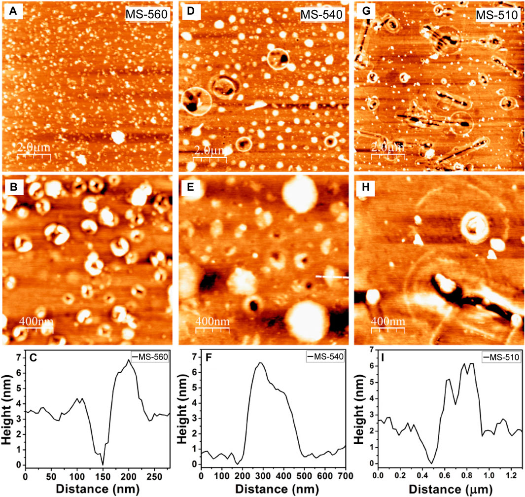
FIGURE 2. AFM images (at different magnifications) and height profile for MoS2 nanodots grown at different substrate temperatures: (A–C) MS-560 (D–F) MS-540 and (G–I) MS-510.
Micro-Raman Studies
Micro-Raman measurements were performed on the as-grown MoS2 dot samples, and it was compared with that of the bulk MoS2 flakes. Figure 3A represents a comparison of the Raman spectra for different samples, which exhibit two important characteristic Raman modes, and this is a signature of the few-layer MoS2, associated with the E2g and A1g phonon modes at 379 and 405 cm−1, respectively. In general, the E2g mode is an in-plane vibration of two S atoms with respect to the Mo atoms, while the A1g mode is associated with the out-of-plane vibration of only S atoms in opposite directions with respect to the Mo atoms. These two Raman modes are very sensitive to the local in-plane, edge defects, and impurities present on the atomic layers of MoS2. The separation between these two modes is a measure of the number of layers in the MoS2. It is clear from Figure 3A that a few-layer MoS2 has been grown for samples MS-560, MS-540, and MS-510 as evidenced by the presence of E2g and A1g Raman bands, which is also consistent with the FESEM images (Figures 1A–D). On the other hand, in the case of sample MS-310, there was no signature of the MoS2 layer, as evidenced by the absence of the A1g peak in the Raman spectrum. The Raman spectrum of MS-310 shows a strong Raman peak at 338 cm−1, which signifies the presence of MoO3 and negligible presence of S. We also observed a phonon mode stiffening of the characteristic Raman modes, reflected by a blue shift of both the peaks by 3–5 cm−1 for all the as-grown samples. The blue shift is expected to be closely related to the compressive strain induced by the adlayer-substrate lattice mismatch (Hui et al., 2013). The line shape parameters of Raman peaks are shown in Table 1, which depicts the peak position and frequency difference (Δk) between the A1g and E2g. The observed Δk values signify the growth of bilayer and trilayer MoS2. The Lorentzian line shape was fitted for the E2g and A1g bands, as shown in Figure 3B. There are two new Raman bands fitted at the lower and higher frequency side at 380 and 415 cm−1, respectively. An earlier report suggests that the splitting of the A1g peak into two peaks is due to the appearance of a Raman inactive mode (B1u) at 415 cm−1, which is not prominent in the case of bulk MoS2. However, it becomes significant in the case of monolayer MoS2, which makes the A1g peak (406.9 cm−1) asymmetric towards a higher wavenumber. (Li et al., 2012b). The observed splitting in the E2g Raman mode at 380 cm−1 can be attributed to the mechanical strain in the MoS2 dots. (Conley et al., 2013). Note that the symbols represent the experimental data, and blue solid lines signify the fitted data in Figures 3B,E.
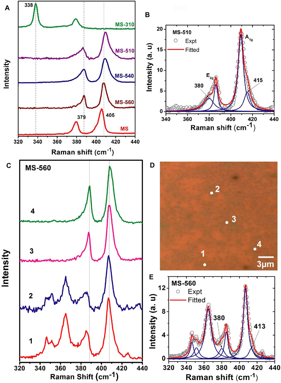
FIGURE 3. (A) Raman fingerprints of as-grown MoS2 dots grown at different substrate temperatures. (B) Lorentzian line shape fitting of E2g and A1g modes in MS-510. Note that the peak center of each mode is denoted in cm−1 unit. (C) Position-dependent Raman spectra of the MS-560 sample, and (D) the corresponding optical micrograph image showing the scanned region for each spectrum marked with the respective serial number. (E) Lorentzian line shape fitting of E2g and A1g modes in MS-560 (position 1) along with the additional Raman modes. These spectra were recorded with 488 nm excitation.
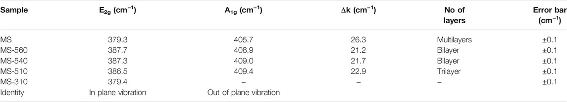
TABLE 1. Summary of the peak positions of E2g and A1g Raman modes and their separation (Δk) signifying the growth of bi-layer and a tri-layer MoS2.
Figures 3C,D show the position-dependent Raman spectra of the as-grown MoS2 dot array in MS-560 and the corresponding OM image showing the scanned area for each spectrum marked with the respective serial number. We observed that the Raman spectra for different locations of a sample show quite similar features. In spots 1 and 2, we found that the frequency difference Δk between the Raman bands is ∼21.5 cm−1 and 21.9 cm−1, respectively, which implies the presence of bilayer MoS2. However, at spots 3 and 4, the frequency differences Δk are found to be 20.2 and 19.9 cm−1, respectively, which implies the coverage of few layers to monolayer MoS2. We notice a shift of the E2g mode without any significant shift of the A1g mode for different spots of the sample MS-560. The summary of the peak parameters is shown in Table 2. There are some additional Raman bands at 346.3, 351.6, and 365.3 cm−1, which are assigned to the stretching modes of the doubly coordinated oxygen (Mo−O−Mo). The observed Raman bands of MoO3 and MoO2 compare well with the reported literature values. (Dieterle and Mestl, 2002). Note that MoO2 and MoO3 are present in the sample due to low-temperature growth.
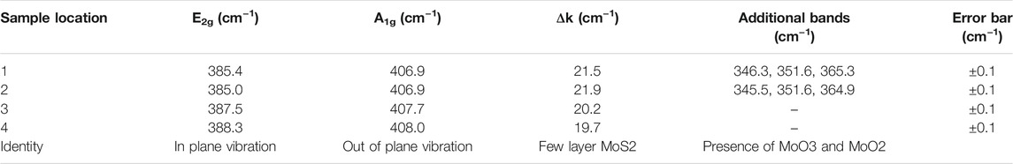
TABLE 2. E2g and A1g Raman modes at different locations of MS-560 and their peak separation significant for the growth of monolayer and bi-layer MoS2.
Position-dependent Raman spectra of as-grown MoS2 dots in MS-540 show similar uniformity and growth of monolayer and bilayer MoS2 dots, as shown in Supplementary Figure S2; Supplementary Table S2. There is also the presence of an additional band corresponding to the MoO2 and MoO3 phases (see Supplementary Figure S2; Supplementary Table S2). In the case of MS-510, we observed mostly trilayer and multi-layered MoS2 growth (Supplementary Figure S2; Supplementary Table S3, ). In this case, the E2g mode is downshifted substantially. Thus, growth at 540–560°C is suitable for the growth of monolayer and bilayer MoS2. However, there are recent research works that have been progressing on low temperature CVD growth in which a new root is being proposed using the atmospheric CVD technique to grow monolayers of MoS2 at 550°C by using sodium (Na) as the catalyst. (Safeer et al., 2021). Authors have produced single and polycrystalline films by controlling the NaNo3/MoO3 catalyst/precursor ratio and growth time. Based on the first-principle calculations, authors have determined that Na was the nucleation site for the growth of MoS2, and the precursor’s ratio is crucial to decrease the formation energy and growth temperature. In the present case, the additional Raman bands associated with the E2g mode; all the samples are attributed to the nucleation sites of MoO3/MoO2 that may be more favorable for the sulfurization process in order to form MoS2 nanodots at low-temperature regimes i.e., 510, 540, and 560°C.
XPS Studies
Figure 4 shows the core level XPS spectra of the Mo-3d and S-2p bands for the as-grown MoS2 dots grown at different substrate temperatures. In Figures 4A,B, several Mo 3d5/2 peaks could be fitted for each Mo (3d) envelope, indicating that more than one Mo species was present. In most of the spectra, the main Mo component (Mo4+) was MoS2. Besides MoS2, all the samples contain additional Mo (3d) peaks corresponding to the oxides of the Mo metal (Mo6+). Note that the peak positions and local environment of S induced surface defects, and impurities were estimated from the Gaussian line shape of the Mo (3d) and S (2p) core level peaks, and the fitting parameters along with the peak identity are summarized in Table 3. Note that the as-grown MS-560 and MS-510 show quite similar spectra. However, in the case of MS-310 (Figure 4C), we notice that the peak intensity corresponding to MoO3 is much higher than that corresponding to MoS2, and the sulfur (2s) peak is absent. This may be due to the higher content of the physisorbed oxygen. Note that MS-310 is grown at a very low temperature, and due to the low vapor pressure of S, the formation of the MoO3 phase dominates.
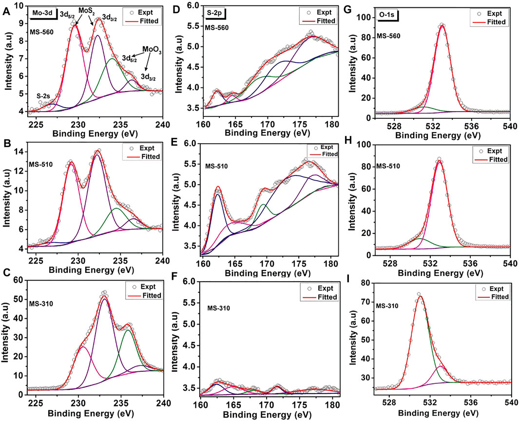
FIGURE 4. Core level XPS spectra and the Shirley line shape fitting of: (A–C) Mo-3d (3d5/2, 3d3/2), (D–F) S-2p (2p3/2, 2p1/2) and (G–I) O-1s for MoS2 dots grown at different substrate temperatures. The peak center in each case is denoted in the eV unit.
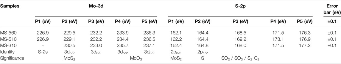
TABLE 3. Summary of the core level XPS peaks of Mo-3d and S-2p bands deconvoluted with Gaussian line shapes.
Figures 4D–F shows the core level XPS S-2p spectra for the as-grown MoS2 dots. The band that is observed in S-2p is the 2p3/2, which is significant for the crystalline S bonded with Mo. The S-2p spectra for all the as-grown samples show the presence of a number of S components. The content of S in all the samples is found to be very low. For MS-310, the amount of S is found to be much less than that of MS-560 and MS-510. This may be due to the lack of formation of MoS2, which is consistent with the Raman spectra discussed earlier. Additionally, we found some new XPS bands in the range 160–180 eV that may be due to the S-related defects. It is expected from the CVD-grown samples that the additional bands from the 2p3/2 may be due to the S or Mo complexes. Due to low substrate temperature, the formation of polysulphides and ionized S (due to the weak bonding with Mo) is quite expected. The higher binding energy of S-2p peaks may correspond to the polysulphide or thiomolybdate (Spevack and McIntyre, 1993) (which has a core structure of MoxSy where x ≠ y < 1) species. There may also be a formation of oxysulphide species, where S-O bonding is present, and this would produce the intense XPS bands in the range 167–170 eV. We also observed some additional peaks in the range 170–180 eV, which may be due to the presence of some impurities.
Figures 4G–I show the core level O-1s XPS spectra for the as-grown MoS2 dots. The O-1s spectrum has been fitted by two peaks (components) for all the samples. The peak position and the intensity ratio are summarized in Table 4. The peaks P1 and P2 are associated with the physisorbed oxygen and SiO2, respectively. We see that the ratio of the intensities of peaks P1/P2 for MS-560 is 0.11 and MS-510 is 0.17, while for MS-310 it is 6.44. This clearly reveals the presence of a higher content of physisorbed oxygen in the case of MS-310. This is consistent with the Mo (3d) XPS spectra, where we observed the presence of a higher integrated intensity of the Mo species associated with the MoO3 (see Figure 4, peaks at 235.7 and 237 1eV). This is also consistent with the Raman analysis that showed the presence of the characteristic peak of MoO3 (Figure 2A).
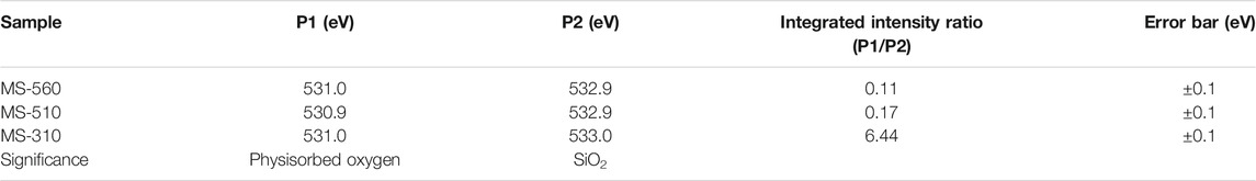
TABLE 4. Summary of the XPS peak positions and their integrated intensity ratios for O-1s spectra of different samples.
Photoluminescence Studies
The as-grown MoS2 dots show strong visible PL at room temperature. Figure 5A shows the PL spectra of the MoS2 dots grown at different substrate temperatures (MS-560, MS-540, and MS-510) along with that of the commercial MoS2 flakes (MS). We observed a clear blue shift in the PL peak positions for the MS-560, MS-540, and MS-510 with respect to that of bulk MoS2. The blue shift is maximum for the MS-560 sample, which is due to the direct band gap transition in the monolayer MoS2, consistent with the previous reports. (Splendiani et al., 2010; Nan et al., 2014). Furthermore, the intensity of PL in MoS2 dots is about one order of a magnitude higher than that of the bulk MoS2 flakes. The strongly enhanced PL is direct evidence for the direct bandgap nature of the MoS2 dots, as compared to the indirect gap of the bulk MoS2. In order to understand the origin of the PL band, we have deconvoluted each spectrum of the MoS2 dot sample by using four Gaussian peaks (Figures 5B–D). The summary of the peak positions in each sample is listed in Table 5. Two characteristic PL peaks, P1 and P2, centered at ∼ 621–631 nm and ∼660–667 nm are ascribed to B exciton and A exciton, respectively. (Splendiani et al., 2010). An exciton peak is derived from the direct bandgap of MoS2, and the B exciton peak arises from the direct gap transition between the minima of the conduction band and the lower-level valence band maxima that is created by strong valence-band spin-orbit splitting at the K point (Splendiani et al., 2010). We also observed the presence of the A− exciton (P3) peak, which is understood as arising from the trions. The trion emission is caused by light n-type doping from the substrate or from charged impurities in the CVD-grown MoS2 dots. (Tongay et al., 2013; Dhakal et al., 2014). We also observed the presence of peak P4 in all the samples at ∼ 696–700 nm, and this peak is attributed to the radiative recombination of bound excitons. (Tongay et al., 2013). This defect peak may be due to the presence of S vacancies in the samples. Note that the relative intensity of P4 is higher in the case of MS-510, than the other two samples. This is because of the lower temperature growth. All four peaks have been observed only in MS-560, MS-540, and MS-510. On the other hand, MS-310 did not show any PL, consistent with the lack of formation of MoS2 as evidenced from the Raman and XPS spectra discussed earlier. We notice a small change in peak positions with the growth temperatures (see Table 5), which could be due to the non-uniformity in layer numbers for different samples.
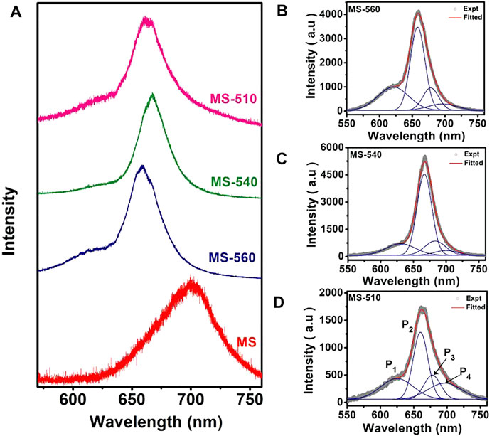
FIGURE 5. (A) Comparison of the PL spectra of MoS2 flakes and MoS2 dots grown at different substrate temperatures. (B–D) PL spectra fitted with four Gaussian peaks (P1, P2, P3, and P4) for MS-560, MS-540, and MS-510, respectively. Note that the PL spectra were recorded with 488 nm laser excitation.
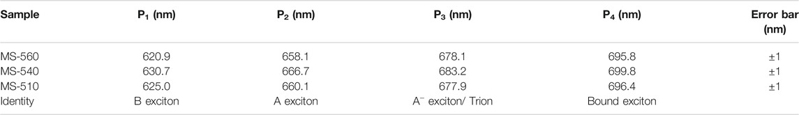
TABLE 5. Summary of the PL peaks deconvoluted from the Gaussian line shape of the measured spectra for the different samples.
Figures 6A,B show the position-dependent PL spectra of the MS-560 sample and the corresponding optical micrograph image showing the scanned area for each spectrum marked with a serial number. We observed that there is a no substantial shift in the PL peak position for different locations of the same sample, indicating fairly uniform growth of the MoS2 dots. A marginal shift in the peak position at location 3 may be due to a small variation in the thickness of the MoS2 dots. Previous reports suggest that the P2 peak is blue-shifted, and the PL intensity is increased when decreasing the thickness from multilayer to monolayer MoS2 films. (Mohapatra et al., 2016). Note that at positions 1 and 2, the integrated PL intensity ratio of the P2/P1 peak is much higher than that at the positions 3 and 4. We also observe a slight broadening of the PL peak in positions 3 and 4, and this may be due to the high trion emission, as the integrated intensity ratio of the P2/P1 peak is lowest in region 4. The P2 peak decreases in intensity due to the enhanced nonradiative decay when MoS2 is doped with electrons. Since the growth is carried out at a relatively low temperature, the presence of structural defects and strain cannot be ignored. MS-540 and MS-510 samples show PL similar to that of MS-560 (see Supplementary Figures S3, S4). This visible PL at room temperature is a direct consequence of the direct gap nature of bilayer MoS2. Thus, our results demonstrate that the CVD growth of an array of monolayer MoS2 dots is possible at a temperature as low as 560°C. Note that monolayer CVD growth of MoS2 is typically achieved at ∼1000°C, though the recent report shows that it can be grown at 680°C. However, the present report shows that monolayer CVD growth is achieved at 560°C.
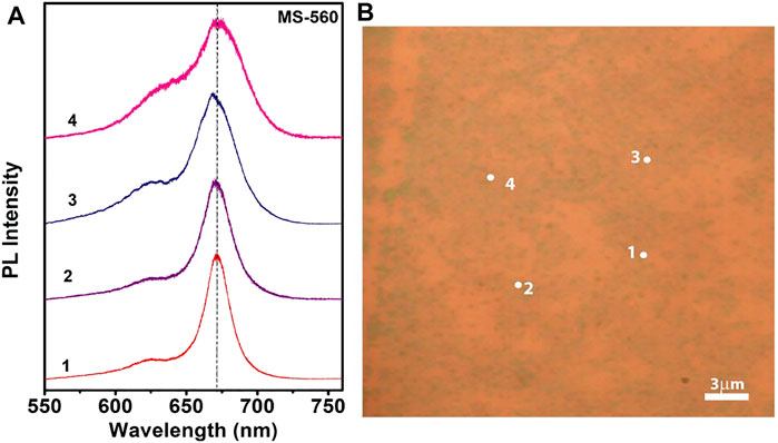
FIGURE 6. (A) Position-dependent PL spectra of the as-grown MoS2 dots (MS-560) and (B) the corresponding OM image showing the scanned area for each spectrum marked with a serial number. Note that the PL spectra were recorded with 488 nm laser excitation.
Growth Mechanism
The growth mechanism of MoS2 nanodots on the SiO2 substrate is shown in Figure 7. Here, MoO3 and sulfur are the precursors used and are placed at a particular distance away from the substrate as mentioned earlier. As the temperature of the single-zone furnace is ramped up to 800°C, first, the MoO3 vapor is partially transferred by the Ar carrier gas and the MoO3 molecules get attached onto the substrates. Next, as the sulfur vaporization takes place, the S atoms appear later near the substrates and react with the MoO3 atoms adhered onto the substrate, resulting in the formation of MoS2 (2MoO3+ 7S2→ MoS2 + 3SO2). However, as the substrates are placed at the region of lower temperatures (510–560°C), due to the short diffusion length on the surface, the MoS2 nanodots grown on the SiO2 substrates are of non-uniform thickness, with a few tens of layers at the center. (Mun et al., 2016c). Additionally, the high flow rate of the Ar carrier gas throughout the experiment has also resulted in the formation of a uniform array of the MoS2 nanodots.
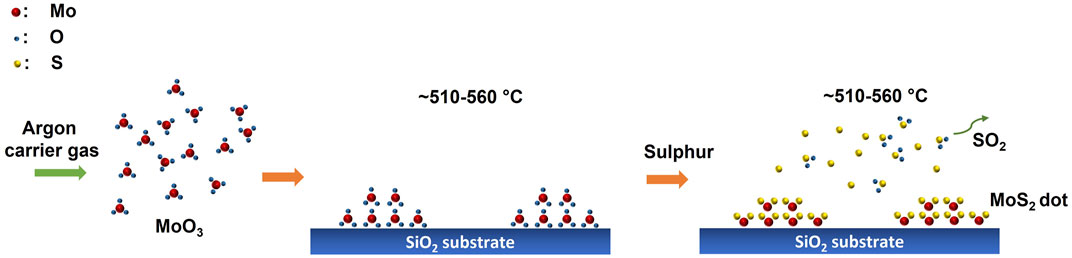
FIGURE 7. A schematic illustration of the growth mechanism of MoS2 nanodots.
Conclusion
Growth of highly luminescent bilayer and few-layer MoS2 dots with controlled size and shape by a low-temperature (510–560°C) CVD technique was reported. The intense visible PL at room temperature with free excitonic emission indicated the direct gap nature of the crystalline MoS2 dots array. Sulfur-induced surface defects are found and detected from the micro-Raman and XPS studies and correlated with the bound excitonic emission in the PL spectrum. Position-dependent Raman and PL profiles showed uniformity in the MoS2 layer for the growth at 540 and 560°C, while some nonuniformity in the MoS2 layer was apparent for growth at 510°C. We believe the low-temperature growth of the luminescence MoS2 dots array will stimulate further studies on growth on flexible substrates and its diverse range of applications in optoelectronics, bioimaging, and related areas.
Data Availability Statement
The original contributions presented in the study are included in the article/Supplementary Material; further inquiries can be directed to the corresponding authors.
Author Contributions
The work was conceived by all three authors. RKB and LPLM primarily conducted the experiments and analysis, and PKG interpreted the results. The manuscript was written and reviewed by all three authors.
Funding
We acknowledge the financial support from CSIR (Grant No. 03(1270)/13/EMR-II), MEITY (Grant No. 5(9)/2012-NANO (Vol.II)) for carrying out part of this work.
Conflict of Interest
The authors declare that the research was conducted in the absence of any commercial or financial relationships that could be construed as a potential conflict of interest.
Publisher’s Note
All claims expressed in this article are solely those of the authors and do not necessarily represent those of their affiliated organizations, or those of the publisher, the editors, and the reviewers. Any product that may be evaluated in this article, or claim that may be made by its manufacturer, is not guaranteed or endorsed by the publisher.
Acknowledgments
We acknowledge Dr. Gavinolla Srinivas Reddy, for his help in conducting the FESEM measurements. We acknowledge central instrumental facility, IIT Guwahati for providing various characterizations techniques such as Raman spectroscopy, AFM facility.
Supplementary Material
The Supplementary Material for this article can be found online at: https://www.frontiersin.org/articles/10.3389/fnano.2021.775732/full#supplementary-material
References
Bernardi, M., Palummo, M., and Grossman, J. C. (2013). Extraordinary Sunlight Absorption and One Nanometer Thick Photovoltaics Using Two-Dimensional Monolayer Materials. Nano Lett. 13 (8), 3664–3670. doi:10.1021/nl401544y
Biroju, R. K., Das, D., Sharma, R., Pal, S., Mawlong, L. P. L., Bhorkar, K., et al. (2017). Hydrogen Evolution Reaction Activity of Graphene-MoS2 van der Waals Heterostructures. ACS Energ. Lett. 2, 1355–1361. doi:10.1021/acsenergylett.7b00349
Biroju, R. K., Pal, S., Sharma, R., Giri, P. K., and Narayanan, T. N. (2017). Stacking sequence dependent photo-electrocatalytic performance of CVD grown MoS2/graphene van der Waals solids. Nanotechnology 28, 085101. doi:10.1088/1361-6528/aa565a
Conley, H. J., Wang, B., Ziegler, J. I., Haglund, R. F., Pantelides, S. T., and Bolotin, K. I. (2013). Bandgap Engineering of Strained Monolayer and Bilayer MoS2. Nano Lett. 13 (8), 3626–3630. doi:10.1021/nl4014748
Dhakal, K. P., Duong, D. L., Lee, J., Nam, H., Kim, M., Kan, M., et al. (2014). Confocal Absorption Spectral Imaging of MoS2: Optical Transitions Depending on the Atomic Thickness of Intrinsic and Chemically Doped MoS2. Nanoscale 6 (21), 13028–13035. doi:10.1039/c4nr03703k
Dieterle, M., and Mestl, G. (2002). Raman Spectroscopy of Molybdenum Oxides. Phys. Chem. Chem. Phys. 4 (5), 822–826. doi:10.1039/b107046k
Feng, J., Qian, X., Huang, C.-W., and Li, J. (2012). Strain-engineered Artificial Atom as a Broad-Spectrum Solar Energy Funnel. Nat. Photon 6 (12), 866–872. doi:10.1038/nphoton.2012.285
Fontana, M., Deppe, T., Boyd, A. K., Rinzan, M., Liu, A. Y., Paranjape, M., et al. (2013). Electron-hole Transport and Photovoltaic Effect in Gated MoS2 Schottky Junctions. Sci. Rep. 3, 1634. doi:10.1038/srep01634
Ganatra, R., and Zhang, Q. (2014). Few-Layer MoS2: A Promising Layered Semiconductor. ACS Nano 8 (5), 4074–4099. doi:10.1021/nn405938z
Gong, C., Huang, C., Miller, J., Cheng, L., Hao, Y., Cobden, D., et al. (2013). Metal Contacts on Physical Vapor Deposited Monolayer MoS2. ACS Nano 7 (12), 11350–11357. doi:10.1021/nn4052138
Gong, Y., Li, B., Ye, G., Yang, S., Zou, X., Lei, S., et al. (2017). Direct Growth of MoS 2 Single Crystals on Polyimide Substrates. 2d Mater. 4, 021028. doi:10.1088/2053-1583/aa6fd2
Hui, Y. Y., Liu, X., Jie, W., Chan, N. Y., Hao, J., Hsu, Y.-T., et al. (2013). Exceptional Tunability of Band Energy in a Compressively Strained Trilayer MoS2 Sheet. ACS Nano 7 (8), 7126–7131. doi:10.1021/nn4024834
Jeon, J., Jang, S. K., Jeon, S. M., Yoo, G., Jang, Y. H., Park, J.-H., et al. (2015). Layer-controlled CVD Growth of Large-Area Two-Dimensional MoS2films. Nanoscale 7 (5), 1688–1695. doi:10.1039/c4nr04532g
Lee, H. S., Min, S.-W., Chang, Y.-G., Park, M. K., Nam, T., Kim, H., et al. (2012). MoS2 Nanosheet Phototransistors with Thickness-Modulated Optical Energy Gap. Nano Lett. 12 (7), 3695–3700. doi:10.1021/nl301485q
Lee, Y.-H., Zhang, X.-Q., Zhang, W., Chang, M.-T., Lin, C.-T., Chang, K.-D., et al. Adv. Mater. 24, 2320–2325.
Li, H., Yin, Z., He, Q., Li, H., Huang, X., Lu, G., et al. (2012). Fabrication of Single- and Multilayer MoS2 Film-Based Field-Effect Transistors for Sensing NO at Room Temperature. Small 8 (1), 63–67. doi:10.1002/smll.201101016
Li, H., Zhang, Q., Yap, C. C. R., Tay, B. K., Edwin, T. H. T., Olivier, A., et al. (2012). From Bulk to Monolayer MoS2: Evolution of Raman Scattering. Adv. Funct. Mater. 22 (7), 1385–1390. doi:10.1002/adfm.201102111
Liu, H. F., Wong, S. L., and Chi, D. Z. (2015). CVD Growth of MoS2-Based Two-Dimensional Materials. Chem. Vapor Deposition 21 (10-11-12), 241–259. doi:10.1002/cvde.201500060
Mak, K. F., He, K., Lee, C., Lee, G. H., Hone, J., Heinz, T. F., et al. (2013). Tightly Bound Trions in Monolayer MoS2. Nat. Mater 12 (3), 207–211. doi:10.1038/nmat3505
Mak, K. F., Lee, C., Hone, J., Shan, J., and Heinz, T. F. (2010). Atomically ThinMoS2: A New Direct-Gap Semiconductor. Phys. Rev. Lett. 105 (13), 136805. doi:10.1103/physrevlett.105.136805
Mohapatra, P. K., Deb, S., Singh, B. P., Vasa, P., and Dhar, S. (2016). Strictly Monolayer Large Continuous MoS2 Films on Diverse Substrates and Their Luminescence Properties. Appl. Phys. Lett. 108, 042101. doi:10.1063/1.4940751
Mun, J., Kim, Y., Kang, I.-S., Lim, S. K., Lee, S. J., Kim, J. W., et al. (2016). Low-temperature Growth of Layered Molybdenum Disulphide with Controlled Clusters. Sci. Rep. 6, 21854. doi:10.1038/srep21854
Mun, J., Kim, Y., Kang, I.-S., Lim, S. K., Lee, S. J., Kim, J. W., et al. (2016). Low-temperature Growth of Layered Molybdenum Disulphide with Controlled Clusters. Sci. Rep. 6, 21854. doi:10.1038/srep21854
Mun, J., Kim, Y., Kang, I.-S., Lim, S. K., Lee, S. J., Kim, J. W., et al. (2016). Low-temperature Growth of Layered Molybdenum Disulphide with Controlled Clusters. Sci. Rep. 6, 21854. doi:10.1038/srep21854
Muratore, C., Hu, J. J., Wang, B., Haque, M. A., Bultman, J. E., Jespersen, M. L., et al. (2014). Continuous Ultra-thin MoS2 Films Grown by Low-Temperature Physical Vapor Deposition. Appl. Phys. Lett. 104 (26), 261604. doi:10.1063/1.4885391
Nan, H., Wang, Z., Wang, W., Liang, Z., Lu, Y., Chen, Q., et al. (2014). Strong Photoluminescence Enhancement of MoS2 through Defect Engineering and Oxygen Bonding. ACS Nano 8 (6), 5738–5745. doi:10.1021/nn500532f
Radisavljevic, B., Radenovic, A., Brivio, J., Giacometti, V., and Kis, A. (2011). Single-Layer MoS2 Transistors. Nat. Nano 6 (3), 147–150. doi:10.1038/nnano.2010.279
Rao, C. N. R., and Nag, A. (2010). Inorganic Analogues of Graphene. Eur. J. Inorg. Chem. 2010 (27), 4244–4250. doi:10.1002/ejic.201000408
Safeer, S. H., Moutinho, M. V. O., Barreto, A. R. J., Archanjo, B. S., Pandoli, O. G., Cremona, M., et al. (2021). Sodium-Mediated Low-Temperature Synthesis of Monolayers of Molybdenum Disulfide for Nanoscale Optoelectronic Devices. ACS Appl. Nano Mater. 4 (4), 4172–4180. doi:10.1021/acsanm.1c00491
Spevack, P. A., and McIntyre, N. S. (1993). A Raman and XPS Investigation of Supported Molybdenum Oxide Thin Films. 2. Reactions with Hydrogen Sulfide. J. Phys. Chem. 97 (42), 11031–11036. doi:10.1021/j100144a021
Splendiani, A., Sun, L., Zhang, Y., Li, T., Kim, J., Chim, C.-Y., et al. (2010). Emerging Photoluminescence in Monolayer MoS2. Nano Lett. 10 (4), 1271–1275. doi:10.1021/nl903868w
Tongay, S., Suh, J., Ataca, C., Fan, W., Luce, A., Kang, J. S., et al. (2013). Defects Activated Photoluminescence in Two-Dimensional Semiconductors: Interplay between Bound, Charged and Free Excitons. Sci. Rep. 3, 2657. doi:10.1038/srep02657
Ye, Y., Ye, Z., Gharghi, M., Yin, X., Zhu, H., Zhao, M., et al. (2014). Exciton-related Electroluminescence from Monolayer MoS2. San Jose, California: CLEOOptical Society of America. 2014/06/08, 2014STh4B.4.
Yin, Z., Li, H., Li, H., Jiang, L., Shi, Y., Sun, Y., et al. (2012). Single-Layer MoS2 Phototransistors. ACS Nano 6 (1), 74–80. doi:10.1021/nn2024557
Yu, J., Li, J., Zhang, W., and Chang, H. (2015). Synthesis of High Quality Two-Dimensional Materials via Chemical Vapor Deposition. Chem. Sci. 6 (12), 6705–6716. doi:10.1039/c5sc01941a
Zeng, Z., Yin, Z., Huang, X., Li, H., He, Q., Lu, G., et al. (2011). Single-Layer Semiconducting Nanosheets: High-Yield Preparation and Device Fabrication. Angew. Chem. Int. Ed. 50 (47), 11093–11097. doi:10.1002/anie.201106004
Zhang, H. (2015). Ultrathin Two-Dimensional Nanomaterials. ACS Nano 9 (10), 9451–9469. doi:10.1021/acsnano.5b05040
Zhang, J., Yu, H., Chen, W., Tian, X., Liu, D., Cheng, M., et al. (2014). Scalable Growth of High-Quality Polycrystalline MoS2 Monolayers on SiO2 with Tunable Grain Sizes. ACS Nano 8 (6), 6024–6030. doi:10.1021/nn5020819
Keywords: MoS2 dots, photoluminescence, low temperature CVD, defect engineering, transition metal dichacogenides
Citation: Mawlong LPL, Biroju RK and Giri PK (2021) Low-Temperature Chemical Vapor Deposition Growth of MoS2 Nanodots and Their Raman and Photoluminescence Profiles. Front. Nanotechnol. 3:775732. doi: 10.3389/fnano.2021.775732
Received: 14 September 2021; Accepted: 03 November 2021;
Published: 30 November 2021.
Edited by:
Yizhou Zhang, Nanjing University of Information Science and Technology, ChinaReviewed by:
Illyas Md Isa, Universiti Pendidikan Sultan Idris, MalaysiaJaime Andres Perez Taborda, National University of Colombia, Colombia
Wende Xiao, Beijing Institute of Technology, China
Copyright © 2021 Mawlong, Biroju and Giri. This is an open-access article distributed under the terms of the Creative Commons Attribution License (CC BY). The use, distribution or reproduction in other forums is permitted, provided the original author(s) and the copyright owner(s) are credited and that the original publication in this journal is cited, in accordance with accepted academic practice. No use, distribution or reproduction is permitted which does not comply with these terms.
*Correspondence: Ravi K. Biroju, Ymlyb2p1cmF2aUBnbWFpbC5jb20=; P. K. Giri, Z2lyaUBpaXRnLmVybmV0Lmlu
†These authors have contributed equally to this work