 Taylor Wilson*
 Bertrand Cambou
- School of Informatics Computing and Cyber-Systems, Northern Arizona University, Flagstaff, AZ, United States
In this paper, we present the characterization of pre-formed resistive random access memories to design physical unclonable functions and experimentally validate inherent properties such as tamper sensitivity and a self-destroy mode. The physical unclonable functions were tested for repetitive use, temperature effects, and aging. The variations during successive response generation cycles and drift rates are quantized to explore their reliability. We define tamper-sensitivity as the ability to detect tampering attacks. To establish tamper sensitivity, the cells were characterized for higher current sweeps, and the injected current at which they break down is extracted and analyzed to determine suitable operating ranges. Our experimental results show that at least 91% of the cells can generate keys protected by the scheme, while 22% of the sensing elements are triggered. Finally, the cells were characterized for high Voltage sweeps to be able to destroy the physical unclonable functions on-demand when tampering activity is detected. A fixed Voltage of 1.9 V is enough to destroy the entire array.
1 Introduction
Physical Unclonable Function (PUF) architectures, also known as “Digital fingerprints,” are widely used as a hardware security primitive; their implementations can provide system authentication and key generations on-demand (Suh and Devadas, 2007; Herder et al., 2014). The design of PUFs with Resistive Random-Access Memory (ReRAM) has been widely reported while exploiting either the probabilistic switching of the cells or the resistance variability between the cells after SET/RESET operations. However, such approaches often disturb the cells as conductive filaments (CFs) are repeatedly formed and ruptured while generating Challenge-Response Pairs (CRPs). In return, it leaves behind evident traces of user activity after key generation cycles. Moreover, information is also retained in the form of CFs, which the crypto analyst can potentially exploit to generate secrets using methods such as Differential Power Analysis (DPA). Therefore, there is a need to design low-powered and tamper-sensitive PUFs that do not disturb the technology. In this paper, we present a non-intrusive methodology for the ReRAM technology to design PUFs; by sourcing small currents to the pre-formed array, the cells return differentiated and highly reproducible resistances suitable for cryptographic key generations (Cambou et al., 2017). Here, the residual impacts of the electrical currents are ephemeral, and they are not observable after powering off the cells; to an extent, the applied energy is not strong enough to either influence ion migration or degradation by localized joule-heating. Thus, cycling the cells through small current injections leaves them electrically undisturbed. The PUFs thereby operate in a pristine resistive state (PRS). Conversely, when the cells are submitted to higher currents, they experience drift, resulting in permanent degradation; they can no longer return to their pristine condition. Furthermore, higher currents leave measurable differences in pristine resistances, unlike ReRAM cells operating in the SET/RESET modes. We are proposing to leverage such property to set up the array as a sensing element to detect tampering activities if an unauthorized user does not measure the PUFs correctly. Lastly, when tamper attacks are sensed, a self-destroy protocol can be executed by programming a percentage of the cells on command, rendering the PUFs ineffective for future authentication and key generation cycles.
To study and validate the approach, we stress-tested 4,096 Al2O3-based ReRAM cells to quantify their reliability and robustness as pre-formed ReRAM-based PUFs. First, the PUFs were tested for repeated current sweeps at room temperature and 125°C. Next, the tamper-sensitive and self-destroy protocols are experimentally validated by pushing the cells to higher current and voltage sweeps. Finally, the breakdown values are extracted and analyzed to determine suitable operating ranges for the PUFs. The novelty of this work is utilizing pristine ReRAM as PUFs; by operating in a memory state before electroforming (pre-formed) and at low power, the design is highly reliable, tamper sensitive, and has a self-destroy feature at no additional costs. The paper is organized as follows.
Section 2 provides some background information for this work, which includes the ReRAM and its resistive switching processes (i.e., program/erase cycles), ReRAM-based PUFs, and tamper-sensitive PUFs. Section 3 reports the materials and methods used in this study to characterize the tamper-sensitive pre-formed ReRAM-based PUFs. Finally, Section 4 explores the properties of the ReRAM arrays to anticipate the reliability of the PUFs. For this purpose, we report the variations due to repetitive read cycles, temperature effects, and drifts caused by aging are quantified. Furthermore, the two security countermeasures are experimentally validated; first, a sensing scheme to detect physical tampering with the array. We have uncovered how a large portion of the cells used to generate keys are protected at higher currents while most of the sensing elements would be damaged. Second, with a self-destroy feature, we can destroy many of the cells that generate keys with a fixed Voltage. These cells are observed to be easier to damage with such a feature than the sensing elements, which is desirable.
2 Background information
2.1 Resistive random-access memory technology
With the growing demand for both faster computing and the Internet of Things (IoT), there is a need for alternative memory solutions as conventional charge-based memories are becoming slow and reaching scaling limits. The ReRAM is a promising solution owing to its relatively simple Metal/Insulator/Metal (MIM) structure, low power consumption, multilevel storage, and superior scalability (Zahoor et al., 2020). The basic structure of the ReRAM consists of a switching layer (SL) sandwiched between two electrodes. A cell in a High Resistive State (HRS or “OFF”) (usually greater than ten kilo-ohms) is defined as logic “0.” On the other hand, a cell in a Low Resistive State (LRS or “ON”) (generally less than five kilo-Ohms) is defined as logic “1,” and both states are non-volatile. Representing multiple resistive can be used to increase data storage. The underlying mechanism to either program or reset the cells is based on a resistive switching (RS) process, which causes the formation and rupture of conductive filaments (CFs) and is activated by an applied electric field (E) that drifts charged ions within the SL. The electric field is defined as the ratio of Voltage by oxide thickness (tox). Typically, the ReRAM is pristine after fabrication; an initial electroforming step is required to initiate RS behavior by applying a high Voltage. Two primary RS processes transition a cell from HRS to LRS or vice versa. Valence Change Memory (VCM) is associated with the generation of oxygen vacancies (Vo2+) and the migration of oxygen anions (O2-) to create a defect CF. Our experiments were tested on the other type of ReRAM, Electrochemical Metallization Memory (ECM) (Yang et al., 2009; Dash and Prabaharan, 2019; Stellari et al., 2021; Praveen et al., 2022), and will be used to explain the complete RS process. ECM involves the migration of metal cations to create a metal CF. The basic structure is an active top electrode (TE), intermediate SL, and a passive bottom electrode (BE).
A patterned Aluminum/Alumina/Tungsten (Al/Al2O3/W) structure is used to fabricate the samples characterized in this study. When the cell is subject to a positive Voltage sweep, the active TE properties oxidize and generate Al3+ cations. The Al3+ diffuses through the insulating layer, then gets reduced to Al. The Al atoms nucleate within the SL and build up towards the TE, thus creating a CF. The CF switches the cell from HRS to LRS, referred to as the “SET” process, and the approximate Voltage needed to form is termed, Vset. This process can also be reversed by applying a negative Voltage sweep (for bipolar devices) where the cations dissolve by oxidation; thus, the CF is ruptured. Finally, the cell has transitioned from LRS to HRS, called the “RESET” process, and the Voltage needed to break the CF is Vreset. The BE is inert or chemically inactive through the stages. This process can be repeated to turn ON and OFF the cells by forming and rupturing CFs, respectively. The current state of a cell can be read by applying a small read Voltage, typically 0.1 V, which does not disturb the technology. Here, the two states are distinguishable by a relatively large read margin. Recently, the ReRAM has improved its endurance switching cycles, and additional circuitry has been implemented to detect early failures for improved reliability (Kao et al., 2021).
2.2 Resistive random-access memory-based physical unclonable functions
The formation and rupture of CFs exhibit some levels of stochastic behavior. The critical parameter associated with this effect is the amount of energy applied to the cells, where energy is defined as [Voltage x Current x time] (other factors associated are process variations, device thickness, and type of materials). The energy to form or break CFs will vary across the array. This property can be exploited to design ReRAM PUFs based on probabilistic switching (Koeberl et al., 2013; Rose et al., 2013; Zhang et al., 2014; Chen, 2015; Lin et al., 2021). Common approaches often involve Vset, Vreset, or write times as input parameters to generate responses. For example, in (Chen, 2015), all cells are initially programmed to LRS. Then, a Vreset is applied to the array, where Vreset would ideally reset half of the population, and the other half remain unchanged (or in LRS), thus generating an array of 50–50 1 and 0 states. Due to the stochastic nature of CFs, it can be challenging to control for PUFs, resulting in poor reliability and high error rates. And to mitigate this effect, ReRAM has also been combined with Arbiter PUF (Govindaraj et al., 2018) and Ring Oscillator PUF (Cui et al., 2020). Alternate approaches also exploit the resistance or current variations after SET/RESET operations to increase reliability, where less RS occurs during CRP generation cycles (Chen, 2014; Gao and Ranasinghe, 2017; Kim et al., 2018). However, such designs retain information by creating CFs. Due to the associated ion migration, the resistive states are readily distinguishable and can be read at very low power. As a result, an attacker can generate secrets with enough resources and without the user’s knowledge, compromising the system’s integrity. Therefore, there is a need to design ReRAM PUFs with tamper detection capabilities to prevent unwanted access control. In the next section, we explore existing tamper sensitivity schemes for PUFs.
2.3 Tamper-sensitive resistive random-access memory-based physical unclonable functions
Several tamper detection methodologies have been proposed in the literature to protect PUFs from invasive attacks (Wang and Chen, 2010; Rajendran et al., 2015; Shamsi and Jin, 2016). The methods deter attackers from gaining sensitive information on the PUFs and can alert the client of unauthorized access. Typical approaches often include burying sensitive circuitry beneath layers of metal interconnects and layout obfuscation (Liu et al., 2016), masking bits so that responses are physically hidden (bit concealing) (Yang et al., 2021), or tamper-proof envelopes (Garb et al., 2021) which typically need to be continuously powered. For example, in (Liu et al., 2016), the sense amplifiers (S/A), which read out the responses, are buried beneath the ReRAM array. If the S/A were to be invasively probed by an adversary, they would have to remove the top layer consisting of the ReRAM, which would destroy the interconnects and the PUFs rendering them useless. Although the system’s security is significantly increased, such approaches often require circuit redesigns, leading to increased complexity, power consumption, and area. Therefore, the trade-offs must be considered when implementing this tamper-detection circuitry.
3 Materials and methods
3.1 Experimental setup
The experimental analysis reported in this study was conducted by measuring 180-nm Al2O3-based ReRAM at the wafer level. Complete information regarding the die structure and device layout can be found in (Wilson et al., 2022), including process details, transmission electron microscopy analysis, and the probing equipment used to characterize the cells. Briefly, the cells were probed by a B1500 Agilent Semiconductor Analyzer using a High-Resolution Source Measure Unit (HRSMU) card. On the test chip, the device layout had eighteen devices per row, and each device was addressed individually. In contrast, the remaining devices were left floating as an open circuit to prevent sneaky current paths. Electrical tests performed at 23°C were conducted in ambient temperatures and, at 125°C, used a metal chuck, where the wafer was probed, as a heating element to heat the wafer accordingly.
3.2 Design of pre-formed resistive random-access memory-based physical unclonable functions
The design of a pre-formed ReRAM-based PUF works solely in a pristine resistive state (PRS) and at very low power, below the one to form CF. After fabrication, the ReRAM does not undergo any electroforming or forming cycles, and the cells are characterized as is. No RS will occur during key generation cycles, and the cells will operate in a memory state before forming, hence the term “Pre-formed.” To generate Challenge-Response Pairs (CRPs), each cell in the array is biased with small read currents as the input on the scale of 10 nA to 10 uA, generating various unique resistances per injected current. This property allows each chip to hold quasi-infinite cryptographic secrets with no hardware redesign. The resistance is a function of the Voltage divided by the injected current, measured in Ohms (Ω). Due to uncontrollable process variations (i.e., local defects, traps, and thickness) within the oxide, each cell’s resistance is inherently different and difficult to predict. In addition, currents are forced through the cells in reverse bias, a key factor in reducing cation migration, thus prohibiting ion drifting but still susceptible to hard breakdown by localized joule heating. Initially, each cell undergoes consecutive current sweeps to characterize the array, and their median values are used to define their response within the look-up table, also known as enrollment. Then, the enrollment information with corresponding cell addresses is downloaded into a trusted server, which can be called for future authentication and key generation cycles between server and client.
3.3 Reliability stress tests
The physical elements acting as PUFs are susceptible to drifting effects while subject to repetitive use, temperature effects, and aging, potentially increasing error rates if they have relatively large variations. First, a preliminary analysis was conducted to determine each cell’s relative variability (RV) over fifty consecutive read-cycles at eight injected currents while operating at room temperature and 125 °C conditions. Eq. 1, extracted from (Wilson et al., 2022), quantizes the cycle-to-cycle variations into a percentage, where Rσ and
Next, the drift rate of responses generated at room temperature to 125°C is calculated to understand temperature effects. The resistance drops for increasing temperatures and the opposite for decreasing temperatures, which are normal insulator properties. To calculate the drift rate across two temperatures, first, the cell’s relative distance from the population’s median is calculated using Eqs 2, 3, where the response of a particular cell, i, at some injected current, j, is the input. Finally, the drift rate (in %) can be found by subtracting the value of Eq. 3 from Eq. 2, also represented as Eq. 4. Here, the cells experience little to no drift when holding percentages near zero since they are about the same distance from their respective median at both temperatures. Cells with relatively large drift rates can be masked to reduce bit error rates.
Finally, after the PUFs were characterized for eight currents and two temperatures, the PUFs sat idle for 12 months; then, they were recharacterized to observe aging effects. Here, aging has the potential to change device parameters over time, leading to possible failure. And so, the aging drift rates were calculated similarly to Eq. 4 but across initial and final (aged) responses, as shown in Eqs 5, 6. Note: the “final” response is the aged response, and the drift rate is calculated using Eq. 7. Cells with zero percentages experience no aging since the initial, and aged responses are the same.
3.4 Methods of tamper sensitivity and self-destroy protocols
The underlying mechanism to establish tamper sensitivity differentiates the resistance distribution into two working populations. First, we define a Strong Cell Population (SCP); these cells hold resistances below the array’s median. The reason they are called the SCP is for their robustness. They require a higher injected current to break down relative to cells holding higher resistances, also called the Vulnerable Cell Population (VCP). These cells have resistances above the array’s median. Figure 1 illustrates the device-to-device (D2D) entropy, where 4,096 cells were electrically characterized from 100 nA to 800 nA in 100 nA increments, and the responses generated at 100 nA were extracted. Their corresponding resistances are plotted, ranging from 1 MΩ to 5 MΩ with SCP versus VCP labeled. The D2D variations exhibit high entropy; when read for the same currents, they return to their initial values with little deviation. During enrollment cycles, the threshold resistance is calculated for each injected current, and the addresses of the VCP and SCP are identified. Next, the server downloaded the VCP and SCP information into a look-up table for future key generation cycles. Note: the SCP will operate as usual for key generation cycles. At the same time, the VCP is tracked and masked with a ternary state, “X.”
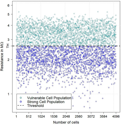
FIGURE 1. Four thousand ninety-six responses generated from an injected current at 100 nA. The array’s median serves as a threshold for each injected current, distinguishing a vulnerable cell population from a strong cell population, called the VCP and SCP, respectively.
As the array was characterized, we observed that the VCP breaks faster than the SCP over increasing current sweeps. This is because the cells must operate below a critical electric field to avoid damage (Cambou and Chen, 2021). Since the oxide thickness is constant across the cells, the critical electric field will also be constant across the cells. The minimum Voltage to begin some breakdown appears to be approximately 1.0 V. Here, the VCP holds critical resistances and will quickly reach this threshold at 1.0 V before the SCP. This effect is illustrated in Figure 2A, where the light blue lines represent the VCP and show a hard breakdown as low as two uA. As the injected current increases, there is a steady decrease in resistance until a hard breakdown occurs. Then, the resistance abruptly drops from a couple of mega-Ohms to less than one kilo-Ohms, which is orders of magnitude difference. The dark blue lines represent the SCP; they can withstand greater current sweeps, hence the “Strong” Cell Population, as shown in Figure 2B. When attackers blindly characterize the PUF array or send random handshakes to observe key generation cycles, the VCP will be triggered into a defective state, thus establishing the VCP as a sensing element. Once the cells have been triggered, returning to a defect-free state is impossible. Therefore, this confirms the effect that pre-formed ReRAM-based PUFs can be used to create a tamper sensitivity scheme.
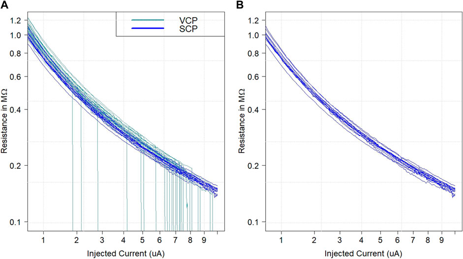
FIGURE 2. Samples of both VCP and SCP undergoing large current sweeps, where (A) shows VCP experiencing a hard breakdown and (B) SCP survives (Cambou and Chen, 2021).
The read margin distinguishing VCP versus SCP is minuscule, around a couple of kilo-Ohms, and the cells near this region exhibit strange behavior. For example, some cells may not break under high current injection stress. Therefore, we propose masking additional SCP near this region. Furthermore, the error rates of the SCP will become relatively lower; therefore, error correction schemes are sufficient to address errors found (Yu and Devadas, 2021; Cambou et al., 2019). The algorithms used to generate keys with the SCP for server and client devices are outlined in (Cambou and Chen, 2021; Cambou et al., 2022).
Finally, we analyze how the SCP can be destroyed by applying a fixed voltage, eliminating the possibility of generating relevant PUF responses. The self-destroy sequence seeks to physically erase a significant portion of the SCP by programming the cells with a particular Vset, thus prohibiting future key generation cycles for any levels of injected currents. The approach is like the probabilistic switching of the cells found in ReRAM-based PUFs, but we do not aim to generate an equal amount 1’s and 0’s across an array, as we only need to destroy a portion of the SCP to drive high BERs. Here, to observe hard breakdown within the SCP, the SCP is subject to Voltage sweeps, ranging from 1.0 to 2.0 V, and applied in 0.05 V increments.
4 Results and discussion
4.1 Relative variability
The responses generated at eight currents, from 100 to 800 nA in 100 nA increments, were extracted to analyze the RV of the PUFs. Figure 3 gives the different box and whisker plots for relative variability percentages versus each injected current at (A) room temperature and (B) 125°C. At room temperature, most responses return percentages in the 0.1%–0.8% range and hold median values around 0.3%, indicating that they do not deviate far from their median values and are thus highly reliable. The same is true for PUFs operating at 125°C but holding higher median values near 0.6%. In addition, notice that the overall variability decreases linearly with higher injected currents for both temperatures. Here, at 100 nA, which generates the noisiest responses, 98.6% of the population return percentages below 2% at room temperature. The outliers above 2% can be considered to exhibit unstable behavior, which can be identified during enrollment and masked with a ternary state not to be used in subsequent key generation cycles. This pre-screening for unstable cells can be key in reducing error rates.
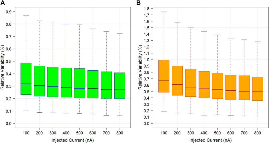
FIGURE 3. Different box and whisker plots for relative variability versus injected currents at (A) room temperature and (B) 125°C.
Furthermore, the PUFs prove robust while operating at higher temperatures. No performance degradation from localized joule heating indicates that the pre-formed ReRAM-based PUFs are highly reliable at 125°C. This characteristic allows the PUFs to operate in the highest military-grade environments. Lastly, when the PUFs are reread for aging, they return to their initial resistances (Section 4.3 reports aging rates). (Supplementary Table S1) reports the quantiles of the RV values for both temperatures. This work statistically validates our previous analysis (Wilson et al., 2022), where only 1,024 cells were characterized for the same currents but at 0°C, 23°C, and 80°C conditions.
4.2 Temperature effects
The responses are drifting approximately the same when operating across different temperatures, as shown in Figure 4, where A, B, C, and D sample the drifting for responses generated at 100, 200, 400, and 800 nA, respectively. The plotted samples represent the entire population.
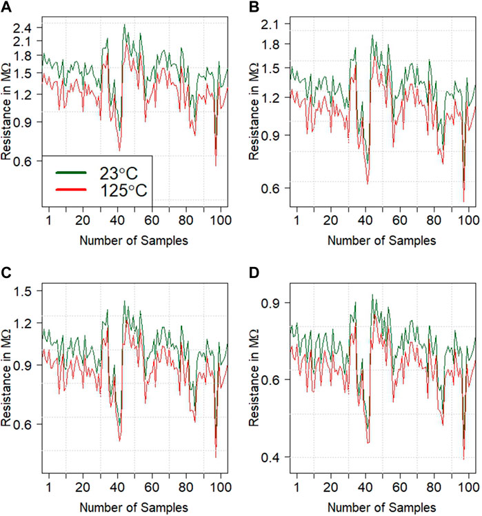
FIGURE 4. Initial versus drifted responses generated at 23°C–125°C for currents at (A) 100 nA, (B) 200 nA, (C) 400 nA, and (D) 800 nA.
The overall drifting effects are summarized in Figure 5, which gives different box and whisker plots for relative drift rate versus eight injected currents. Table 1 reports the drift rates’ quantiles. Here, positive rates indicate that responses are drifting larger distances from the median, whereas with negative rates, they drift less distance from the median. The responses hold median drift rates in the −0.5 to 0.1% ranges for all listed currents indicating that most responses slightly drift above the median. Nonetheless, the responses appear to be drifting the same, considering their median values are near 0%. At 100 nA, 90% of the population holds relative drift rates in the −/+ 4.5% range, which is excellent considering it generates the noisiest responses. While at 800 nA, the relative drift rates quickly shrink as 94% of the population resides within the −/+ 4.5% ranges. The reason is that, at 800 nA, the entropy is far less than that at 100 nA. For example, in Figure 4D, the responses have tighter ranges than 100 nA. Here, the responses have less distance to travel therefore improving the drift rates at higher currents, thus explaining why the population with −/+ 4.5% grows tighter. Finally, the cells having more significant drift rates can be masked to increase the system’s reliability, such as the ones outside the −/+ 4.5% range, which is ∼10% of the population. Future work will explore the effect of temperature on challenge-response pair cycles. If the drift rates are relatively low, then the BER across different temperatures should be low, too, since the general population is drifting approximately the same. Increasing the buffer size (the distance between binary thresholds) can also be implemented to reduce bit errors.
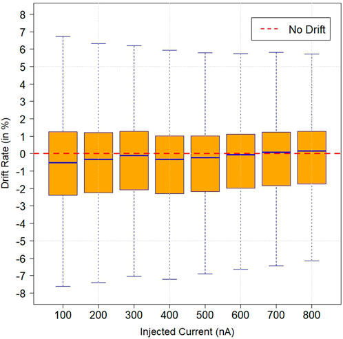
FIGURE 5. Different box and whisker plots for temperature drift rates versus each injected current.
TABLE 1. Quantiles of drift rates for each injected current.
4.3 Aging effects
The aging effects are sampled in Figure 6, which compares the initial versus final (aged) responses generated at 100, 200, 400, and 800 nA in subfigures A, B, C, and D, respectively. Visually, the responses show no obvious signs of performance degradation, as the aged response nearly matches the initial response.
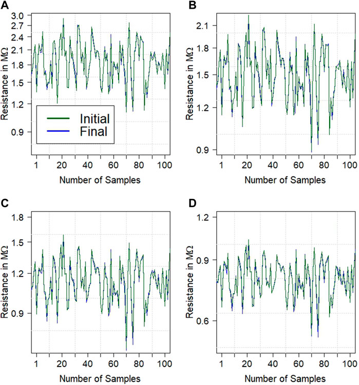
FIGURE 6. Initial versus aged responses at (A) 100 nA, (B) 200 nA, (C) 400 nA, and (D) 800 nA.
The drift rates are summarized in Figure 7, where the relative aging rates versus injected currents are shown in boxplots, and Table 2 reports the quantiles. A positive drift rate indicates that the aged responses read below the initial response, whereas a negative rate reads above the initial response. Cells with relatively large aging rates have the potential to cross their binary threshold leading to bit errors. However, we can model the key generation protocols only to generate bits with a relatively large distance from their binary threshold to anticipate aging rates. This modeling is also true for temperature effects. For example, at 100 nA, 90% of the population returns drift rates in the −/+ 2.5% range, while at 800 nA, 95% drifts within the same rates. Here, cells will only be paired if they have a distance (buffer size) greater than 5% of their median values using cell-pairing methods to generate bits (Cambou 2021). In Figure 7, the median drift rates are in the 0.22 to 0.19% ranges for all listed injected currents indicating that the aging responses slightly read below the initial responses. The variation could be due to the probe needle’s difference in placement on the pads from initial characterizations to the final. Furthermore, the probe needles have faced degradation by strenuous use and aging over time, thus affecting the comparisons. However, the 0.2% variations are insignificant since most cells fall within their normal relative variability ranges of about 2%.
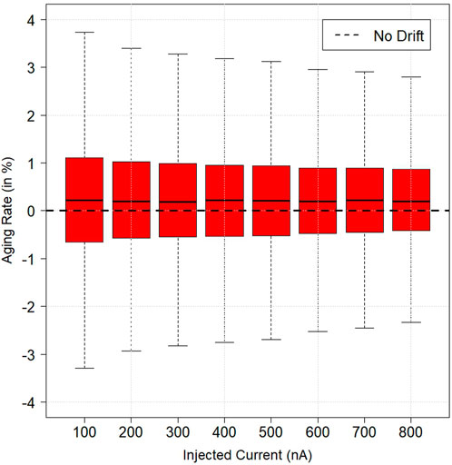
FIGURE 7. Different box and whisker plots for drift rates subject to aging versus each injected current.
TABLE 2. Quantiles of aging rates for each injected current.
4.4 Tamper sensitivity analysis
Four thousand ninety-six new cells were electrically characterized from 100 nA to 10 uA in 50 nA increments. The injected current to break the cells was extracted and plotted against their response generated at 100 nA, as shown in Figure 8. Here, a clear relationship is illustrated; the cells with lower resistances are harder to break. As the current increases, the cells quickly die, which supports our VCP reaching the critical electric field levels before the SCP. A cut-off current can be defined to drive the PUFs to a maximum operating limit. For example, defining a cut-off at 5.5 uA will allow at least 635 pre-formed cells to be destroyed. Of the 635 cells, 453 are attributed to the VCP, while the remaining 182 cells belong to the SCP. Here, 22% of the VCP is destroyed, while at least 91% of the SCP is protected. Note: Additional SCP near the threshold can be masked so that the scheme protects 100% of the SCP.
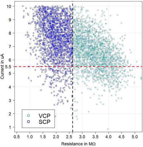
FIGURE 8. Injected currents to break the cells versus resistances extracted at 100 nA.
Table 3 provides a summary of the breakdown analysis for increasing cut-off currents. If an attacker were to characterize the cells to 6 uA, roughly 1,037 cells, or 25% of the total population, would be triggered into a defective state. There are more than enough cells to identify that the array is under invasive attack. Both the SCP and VCP are triggered at alarming rates, driving bit error rates abnormally high. From the client’s standpoint, their array can occasionally be read by a small current (e.g., 100 nA) to check if the VCP has been triggered and monitor if the count is increasing. If so, the attacker is leaving behind apparent traces of tampering, and a self-destroy feature can be initiated by programming the cells. This tamper detection scheme is an additional tool that makes it more difficult to characterize the array unnoticed.
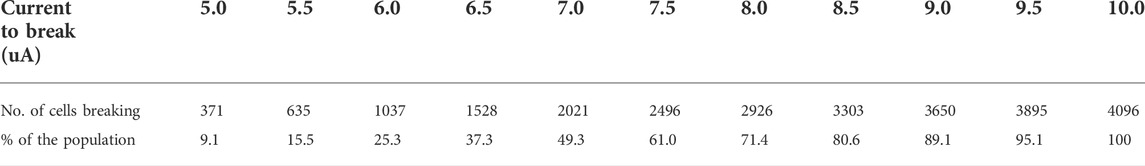
TABLE 3. Sensing Scheme breakdown (for 4,096 cells).
4.5 Self-destroy analysis
In Figure 9, the voltages to break the cells versus their initial response generated at 300 mV are compared, and a summary of the breakdown voltages is provided in Table 4. Applying a fixed 1.35 V to the SCP would destroy roughly 441, or 21%, of the SCP. In this experiment, we do not care about the VCP since they are not used in key generation cycles.
FIGURE 9. Relative breakdown voltages versus initial resistances generated at 300 mV.
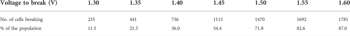
TABLE 4. Self-destroy breakdown (for SCP).
According to Figure 9, applying a fixed voltage at 1.90 V should destroy the entire SCP. So, an additional 4,096 cells were characterized at 100 nA, and the SCP was extracted to verify this effect. The SCP underwent a fixed voltage at 1.90 V with a current compliance of 60 uA (100 us pulse). Again, the cells quickly dropped; in this case, 2048 cells were destroyed (100% of the population), as shown in Figure 10. Here, a sample of healthy responses is shown, and after destroying the PUFs, the responses return values less than one kilo-Ohm for a final readout at 100 nA. When attackers try to observe key generation cycles, they will read useless responses. Notice the large margin between pristine versus destroyed resistances; it is now impossible to generate secrets after a destructive readout. The applied voltages to destroy all the pre-formed ReRAM PUFs occur around 1.90 V and are much less than those reported in similar schemes (Gao et al., 2018), which occur at 4.5 V.
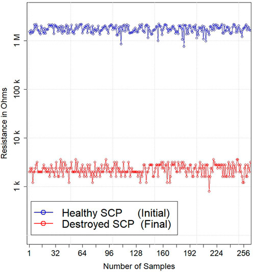
FIGURE 10. Healthy SCP versus Destroyed SCP comparison by applying fixed 1.9 V to array.
5 Conclusion and future work
In this work, we investigated the reliability, tamper-sensitivity, and self-destroy methodologies of a pre-formed ReRAM-based PUF. The PUFs operate near a pristine resistive state, where small currents are injected into the cells and generate a random resistance as the response. First, the PUFs were stress-tested for fifty consecutive current sweeps in the 100–800 nA range in 100 nA increments and two environments (23°C and 125°C). Next, the cycle-to-cycle variations, temperature effects, and aging drifts were quantized. Finally, large current and voltage sweeps were applied to the cells to validate the tamper sensitivity and self-destroy schemes.
Experimental analysis shows that the responses are highly reliable by returning relative variability values in the 0.3% and 0.6% ranges for 23°C and 125°C, respectively. The relative variability decreases over higher currents as well. In addition, there are no obvious signs of performance degradation when read for repetitive use and while operating at 125 °C. For temperature effects, most cells behave in a rather predictive way. At 100 nA, 90% of the population drifts within −/+4.5%, while at 800 nA, it is 94%. A multi-enrollment can be executed at different temperatures to identify and mask unstable cells that are not drifting the same to improve the system’s reliability. For example, cells outside the −/+4.5% range can be masked, about 10% of the cells. Lastly, for aging aspects, at 100 nA, 90% of the population report aging rates in the −/+2.5% range, while at 800 nA, it is 95%. Here, while sitting idle for 12 months, the responses are not showing any signs of degradation but slightly drift below the initial responses, around 0.2%. However, this variation is insignificant since most cells fall within their normal relative variability range of 2%.
The response distributions of each injected current are split into subgroups: the Strong Cell Population (SCP) and the Vulnerable Cell Population (VCP). The scheme increases the system’s reliability and security by only utilizing the SCP for key generation cycles and setting up the VCP as sensing elements to detect physical tampering with the array. Here, the VCP holds critical resistances, thus reaching a critical electric field quicker to experience a hard breakdown relative to the SCP. Experimental analysis shows that the injected currents can drive up to 5.5 uA, where roughly 91% of the SCP is protected, but 20% of the VCP is destroyed. The bit errors within the SCP are small enough to be addressed by ECC. However, additional cells below the threshold can be masked to improve error rates. Lastly, the client can monitor if the VCP has been triggered over time to detect intrusions. Finally, the SCP can be physically destroyed by applying a fixed Voltage at 1.90 V. Here, 100% of the SCP experience irreversible damage preventing relevant response readouts.
For future work, the temperature dataset reported in this study will be used to generate keys with the SCP-only and quantize bit error rates in 256-bit keys. Next, the PUFs need to be characterized for injected currents above 800 nA to 5.5 uA to understand the reliability.
Data availability statement
The raw data supporting the conclusion of this article will be made available by the authors, without undue reservation.
Author contributions
TW performed the experimental testing, analyzed, and discussed the results, and wrote the document. BC developed the concepts and schemes.
Funding
This work was funded by the Air Force Research Laboratory (AFRL) under award number FA8750-19-2-0503.
Conflict of interest
The authors declare that the research was conducted in the absence of any commercial or financial relationships that could be construed as a potential conflict of interest.
Publisher’s note
All claims expressed in this article are solely those of the authors and do not necessarily represent those of their affiliated organizations, or those of the publisher, the editors and the reviewers. Any product that may be evaluated in this article, or claim that may be made by its manufacturer, is not guaranteed or endorsed by the publisher.
Supplementary material
The Supplementary Material for this article can be found online at: https://www.frontiersin.org/articles/10.3389/fnano.2022.1055545/full#supplementary-material
References
Cambou, B., and Chen, Y. C. (2021). “Tamper sensitive ternary ReRAM-based PUFs,” in Intelligent computing (Cham: Springer), 1020–1040.
Cambou, B., Chipana, R., and Habib, B. (2017). PUF with dissolvable conductive paths. US Patent Application US201761541005P.
Cambou, B. (2021). Fast cryptographic key generation from memristor-based physical unclonable functions. US Patent application US20210314176A1.
Cambou, B., Heynssens, J., Burke, I., and Wilson, T. (2022). Sensing Scheme for low power refram-based physical unclonable functions. US Patent application US20220044727A1.
Cambou, B., Philabaum, C., Booher, D., and Telesca, D. A. (2019). “Response-based cryptographic methods with ternary physical unclonable functions,” in Future of Information and Communication Conference (Cham: Springer), 781–800.
Chen, A. (2015). Reconfigurable physical unclonable function based on probabilistic switching of RRAM. Electron. Lett. 51 (8), 615–617. doi:10.1049/el.2014.4375
Chen, A. (2014). Utilizing the variability of resistive random access memory to implement reconfigurable physical unclonable functions. IEEE Electron Device Lett. 36 (2), 138–140. doi:10.1109/led.2014.2385870
Cui, Y., Wang, C., Liu, W., Gu, C., O'Neill, M., and Lombardi, F. (2020). Lightweight configurable ring oscillator PUF based on RRAM/CMOS hybrid circuits. IEEE Open J. Nanotechnol. 1, 128–134. doi:10.1109/ojnano.2020.3040787
Dash, C. S., and Prabaharan, S. R. S. (2019). Nano resistive memory (Re-RAM) devices and their applications. Rev. Adv. Mater. Sci. 58 (1), 248–270. doi:10.1515/rams-2019-0014
Gao, Y., Jin, C., Kim, J., Nili, H., Xu, X., Burleson, W., et al. (2018). Efficient erasable PUFs from programmable logic and memristors. Cryptology ePrint Archive.
Gao, Y., and Ranasinghe, D. C. (2017). R $^ 3$ PUF: A highly reliable memristive device based reconfigurable PUF. arXiv preprint arXiv:1702.07491.
Garb, K., Obermaier, J., Ferres, E., and Künig, M. (2021). “Fortress: FORtified tamper-resistant envelope with embedded security sensor,” in 2021 18th international conference on privacy, security and trust (PST) (IEEE), 1–12.
Govindaraj, R., Ghosh, S., and Katkoori, S. (2018). Design, analysis and application of embedded resistive RAM based strong arbiter PUF. IEEE Trans. Dependable Secure Comput. 17 (6), 1232–1242. doi:10.1109/tdsc.2018.2866425
Herder, C., Yu, M. D., Koushanfar, F., and Devadas, S. (2014). Physical unclonable functions and applications: A tutorial. Proc. IEEE 102 (8), 1126–1141. doi:10.1109/jproc.2014.2320516
Kao, Y. F., Shih, J. R., Lin, C. J., and King, Y. C. (2021). An early detection circuit for endurance enhancement of backfilled contact resistive random access memory array. Nanoscale Res. Lett. 16 (1), 114–119. doi:10.1186/s11671-021-03569-0
Kim, J., Nili, H., Adam, G. C., Truong, N. D., Strukov, D. B., and Kavehei, O. (2018). “Predictive analysis of 3D ReRAM-based PUF for securing the Internet of Things,” in 2018 IEEE region ten symposium (tensymp) (IEEE), 91–94.
Koeberl, P., Kocabaş, Ü., and Sadeghi, A. R. (2013). “Memristor PUFs: A new generation of memory-based physically unclonable functions,” in 2013 Design, Automation & Test in Europe Conference & Exhibition (DATE) (IEEE), 428–431.
Lin, B., Pang, Y., Gao, B., Tang, J., Wu, D., Chang, T. W., et al. (2021). A highly reliable RRAM physically unclonable function utilizing post-process randomness source. IEEE J. Solid-State Circuits 56 (5), 1641–1650. doi:10.1109/jssc.2021.3050295
Liu, R., Wu, H., Pang, Y., Qian, H., and Yu, S. (2016). “A highly reliable and tamper-resistant RRAM PUF: Design and experimental validation,” in 2016 IEEE international symposium on hardware oriented security and trust (HOST) (IEEE), 13–18.
Praveen, P., Rose, T. P., and Saji, K. J. (2022). Top electrode dependent resistive switching in M/ZnO/ITO memristors, M= Al, ITO, Cu, and Au. Microelectron. J. 121, 105388. doi:10.1016/j.mejo.2022.105388
Rajendran, J., Karri, R., Wendt, J. B., Potkonjak, M., McDonald, N., Rose, G. S., et al. (2015). Nano meets security: Exploring nanoelectronic devices for security applications. Proc. IEEE 103 (5), 829–849. doi:10.1109/jproc.2014.2387353
Rose, G. S., McDonald, N., Yan, L. K., and Wysocki, B. (2013). “A write-time based memristive PUF for hardware security applications,” in 2013 IEEE/ACM International Conference on Computer-Aided Design (ICCAD) (IEEE), 830–833.
Shamsi, K., and Jin, Y. (2016). “Security of emerging non-volatile memories: Attacks and defenses,” in 2016 IEEE 34th VLSI test symposium (VTS) (IEEE), 1–4.
Stellari, F., Wu, E. Y., Ando, T., Cartier, E., Frank, M. M., Cabral, C., et al. (2021). Resistive random access memory filament visualization and characterization using photon emission microscopy. IEEE Electron Device Lett. 42 (6), 828–831. doi:10.1109/led.2021.3071168
Suh, G. E., and Devadas, S. (2007). “Physical unclonable functions for device authentication and secret key generation,” in 2007 44th ACM/IEEE Design Automation Conference (IEEE), 9–14.
Wang, X., and Chen, Y. (2010). “Spintronic memristor devices and application,” in 2010 Design, Automation & Test in Europe Conference & Exhibition (DATE 2010) (IEEE), 667–672.
Wilson, T., Cambou, B., Riggs, B., Burke, I., Heynssens, J., and Jo, S. H. (2022). “Design and analysis of pre-formed ReRAM-based PUF,” in Science and information conference (Cham: Springer), 532–549.
Yang, B., Arumí, D., Manich, S., Gómez-Pau, Á., Rodríguez-Montañés, R., González, M. B., et al. (2021). Serial RRAM cell for secure bit concealing. Electronics 10 (15), 1842. doi:10.3390/electronics10151842
Yang, L., Kuegeler, C., Szot, K., Ruediger, A., and Waser, R. (2009). The influence of copper top electrodes on the resistive switching effect in TiO 2 thin films studied by conductive atomic force microscopy. Appl. Phys. Lett. 95 (1), 013109. doi:10.1063/1.3167810
Yu, M. D., and Devadas, S. (2010). Secure and robust error correction for physical unclonable functions. IEEE Des. Test. Comput. 27 (1), 48–65. doi:10.1109/mdt.2010.25
Zahoor, F., Azni Zulkifli, T. Z., and Khanday, F. A. (2020). Resistive random access memory (RRAM): An overview of materials, switching mechanism, performance, multilevel cell (MLC) storage, modeling, and applications. Nanoscale Res. Lett. 15 (1), 90–26. doi:10.1186/s11671-020-03299-9
Keywords: pristine resistive RAM, physical unclonable functions (PUFs), tamper sensitivity, self-destroy mode, hardware security
Citation: Wilson T and Cambou B (2022) Tamper-sensitive pre-formed ReRAM-based PUFs: Methods and experimental validation. Front. Nanotechnol. 4:1055545. doi: 10.3389/fnano.2022.1055545
Received: 27 September 2022; Accepted: 17 October 2022;
Published: 03 November 2022.
Edited by:
Yao-Feng Chang, Intel, United StatesReviewed by:
Yifu Huang, University of Texas at Austin, United StatesYuqian Gu, University of Texas at Austin, United States
Zhongjie Ren, University of Texas at Austin, United States
Junzhe Kang, University of Illinois at Urbana-Champaign, United States
Copyright © 2022 Wilson and Cambou. This is an open-access article distributed under the terms of the Creative Commons Attribution License (CC BY). The use, distribution or reproduction in other forums is permitted, provided the original author(s) and the copyright owner(s) are credited and that the original publication in this journal is cited, in accordance with accepted academic practice. No use, distribution or reproduction is permitted which does not comply with these terms.
*Correspondence: Taylor Wilson, dGpiMzg5QG5hdS5lZHU=