 Miguel Rengifo1,2,3
 Myriam H. Aguirre
 Diego Rubi
- 1Instituto de Nanociencia y Nanotecnología (INN), Comisión Nacional de Energía Atómica-Consejo Nacional de Investigaciones Científicas y Técnicas (CNEA-CONICET), Buenos Aires, Argentina
- 2Departamento de Micro y Nanotecnologías, Comisión Nacional de Energía Atómica (CNEA), San Martín, Argentina
- 3Instituto de Nanociencia y Materiales de Aragón (INMA), Universidad de Zaragoza, Zaragoza, Spain
- 4Departamento de Física de Materia Condensada, Universidad de Zaragoza, Zaragoza, Spain
- 5Laboratorio de Microscopías Avanzada (LMA), Instituto de Nanociencia de Aragón (INA)-Universidad de Zaragoza, Zaragoza, Spain
- 6Centro Atómico Bariloche and Instituto Balseiro, San Carlos de Bariloche, Río Negro, Argentina
- 7CRISMAT, CNRS UMR 6508, ENSICAEN, Caen, France
Neuromorphic computing requires the development of solid-state units able to electrically mimic the behavior of biological neurons and synapses. This can be achieved by developing memristive systems based on ferroelectric oxides. In this work we fabricate and characterize high quality epitaxial BaTiO3-based memristors integrated with silicon. After proving the ferroelectric character of BaTiO3 we tested the memristive response of LaNiO3/BaTiO3/Pt microstructures and found a complex behavior which includes the co-existence of volatile and non-volatile effects, arising from the modulation of the BaTiO3/Pt Schottky interface by the direction of the polarization coupled to oxygen vacancy electromigration to/from the interface. This produces remanent resistance loops with tunable ON/OFF ratio and asymmetric resistance relaxations. These properties might be harnessed for the development of neuromorphic hardware compatible with existing silicon-based technology.
1 Introduction
Modern computers run under the Von Neumann paradigm, where the units that process and store the information are physically separated. This implies an intense data traffic between the processor (CPU) and the memory through a bus that works at a lower frequency than the CPU clock, originating the so-called “memory wall” that limits the computer performance in the case of highly demanding processes such as the training of state-of-the-art neural networks. In addition, these algorithms are extremely energy demanding suggesting that their ever-growing use in modern society might not be sustainable Mehonic and Kenyon (2022). This triggers the search of new computer architectures and data processing paradigms. Among them, a great deal of attention is generated by neuromorphic computing Yu (2017); Mehonic and Kenyon (2022), which intends to develop hardware beyond the Von Neumann concept, able to mimic the extremely efficient and powerful capabilities of the mammals brain. To construct these machines, the development of solid state building blocks able to electrically replicate the behavior of neurons and synapses is needed.
Memristors -defined as metal/insulator/metal micro or nanostructures able to electrically switch between different resistance states [Sawa (2008); Ielmini and Waser (2016)]—are excellent candidates for the latter as different neuromorphic functionalities have been reported Kumar et al. (2022). Memristive mechanisms usually rely on the electromigration of charged point defects such as oxygen vacancies (OV) [(Sawa (2008); Rozenberg et al. (2010)]; however, faster devices might be expected from electronic mechanisms such as the switching of the polarization in the case of ferroelectric memristors. A lot of attention was dedicated to ferroelectric tunnel junctions (FTJs), where an ultrathin ferroelectric material is sandwiched between asymmetric metallic electrodes Tsymbal and Kohlstedt (2006); Garcia et al. (2009); Zhuravlev et al. (2009); Chanthbouala et al. (2012). In this case, the direction of the (switchable) polarization controls the height of the tunnel barrier, leading to different resistive states upon polarization inversion. However, FTJs are difficult to fabricate and their response is usually extremely sensitive to the presence, for instance, of interface roughness or pin-holes in the ferroelectric layer. More robust ferroelectric memristors are found for thicker ferroelectric layers in contact with electrodes with an appropriate work-function in order to form a Schottky barrier Blom et al. (1994); Meyer and Waser (2006); Pintilie et al. (2010). In this case, the direction of the polarization modulates the height of the Schottky barrier and controls the interface resistance. For ferroelectric oxides, it was shown that the ferroelectric memristive switching is coupled to the electromigration of OV to and from Schottky interfaces Ferreyra et al. (2020a), which also influences the interface resistance. The depolarizing field (EDP) was shown to play a key role in the OV dynamics. This mixture of effects was shown, for symmetric devices, to produce remanent resistance loops with distinct behavior in relation to standard (non-ferroelectric) memristors Ferreyra et al. (2020a).
An important issue linked to the development on new micro or nanoelectronic devices is their possible integration with standard Si-based technology. In the case of ferroelectric memristors, the development of epitaxial structures on Si is of paramount importance to simplify the integration with standard electronics while maintaining a high structural quality that warrants good functional properties. For instance, we recall that in polycrystalline BaTiO3 thin films grown on platinized silicon the presence of small grain destabilizes the structural tetragonal distortion and inhibits the appearance of ferroelectricity Román et al. (2017). The obtention of epitaxial ferroeletric perovskites such as BaTiO3 on Si was reported by using appropriate buffers that allow a better structural matching and strain accommodation between the perovskite structure and the cubic Si cell Scigaj et al. (2013; 2016); Lyu et al. (2018). It was shown that the ferroelectric behavior is strongly linked to the perovskite fabrication conditions, which control the degree of tetragonality and, concomitantly, the remanent polarization Lyu et al. (2018).
In this work, we fabricate Si(001)/YSZ/CeO2/LaNiO3/BaTiO3/Pt epitaxial heterostructures and explore their memristive behavior. The high structural quality of the perovskite layers allows maintaining their bulk functional properties, namely the conducting and ferroelectric characters of LaNiO3 and BaTiO3, respectively. Our devices show memristive effects controlled by the modulation of the Schottky-like BaTiO3/Pt interface by both the direction of the ferroelectric polarization and the electromigration of oxygen vacancies to/from the interface. The combination of these effects produces a mixture of non-volatile and volatile memristive behavior that includes the existence of asymmetric resistance relaxations. The results reported here help paving the way for the development of neuromorphic hardware, integrable with standard Si technologies, as our devices can electrically replicate, in the same unit, the behavior of neurons and synapses.
2 Materials and methods
Si(001)/YSZ/CeO2/LaNiO3/BaTiO3 multilayers were deposited by Pulsed Laser Deposition (PLD) assisted with Reflection High Energy Electron Diffraction (RHEED, 20 kV accelereting voltage was used). The optimized temperature growth and pressures were 800°C and 4.0 × 10⁻⁴mbar for YSZ, 800°C and 4.0 × 10⁻⁴ mbar for CeO2, 750°C and 1.5 × 10⁻¹ mbar for LaNiO3 and 750°C and 2.0 × 10⁻² mbar for BaTiO3. The laser repetition rate and fluence were fixed at 2 Hz and 2 J/cm2, respectively. Pt top electrodes were fabricated ex-situ from a combination of optical lithography and sputtering. The thickness and diameter of the top electrodes were 50 nm and 200 μm, respectively. X-ray diffraction experiments were performed with a Panalytical X’Pert Pro MRD diffractometer. Piezoresponse Force Microscopy (PFM) was done with a Veeco Bruker Multimode 8 microscope. Conducting Atomic Force Microscopy (CAFM) was performed with a Bruker(c) Dimension 3100 microscope. Standard atomic force microscopy (AFM) topographies were also recorded with both microscopes. The structural details of the fabricated heterostructures were analyzed by Scanning Transmission Electron Microscopy (STEM) operated in High-Angle Annular Dark Field (HAADF) mode. A FEI Titan3 60–300 microscope, coupled to a Fischione detector, was operated at 300 kV at room temperature with probe corrected beam. Strain maps were obtained by General Phase Analysis (GPA). Chemical composition was analysed by Energy Dispersive X-ray Spectroscopy (EDS). The AZTEC software was used to perform the quantifications. The estimated error in the extracted atomic percentages (at%) was ≈ 2–3%. Electrical measurements were made at room temperature using both a Keithley 2636 Source Measure Unit and an Agilent 4294A LCR-meter, both hooked to a commercial probe station.
3 Results
3.1 Structural characterization
Yttria-stabilised zirconia (YSZ) displays a cubic structure (cell parameter a = 0.512 nm) and presents a lattice mismatch (defined for bottom/upper layers as f = 100 x (ab - au)/ab, where ab and au are the (bulk) cell parameters of the bottom and upper layers, respectively) with Si (also cubic with cell parameter a = 0.543) of f = +5.7%. YSZ grows epitaxially on Si without the need removing the native SiOx layer Lubig et al. (1992) (typically ≈ 1 nm thick) that is spontaneously formed upon air exposure. The CeO2 unit cell is also cubic (cell parameter a = 0.541 nm) and presents a lattice mismatch f = -6.8% with respect to YSZ. The introduction of CeO2 buffers in our heterostructure allows accommodating the large lattice misfit existing between YSZ and the perovskite structure, and also limits the chemical reactivity of YSZ with the first perovskite layer (LaNiO3). We notice that perovskites grow on CeO2 with their (pseudo-)cubes (apc ≈ 0.4 nm) rotated 45° with respect to CeO2 cubes Scigaj et al. (2013) (we recall that
Figure 1 displays a sketch with the stack of the different layers of the Si(001)/YSZ/CeO2/LaNiO3/BaTiO3 heterostructure -the epitaxial relations are [100] BaTiO3 (001) ‖ [100] LaNiO3 (001) ‖ [110] CeO2 (001) ‖ [110] YSZ (001) ‖ [110] Si (001)-, together with the RHEED patterns recorded, in a single process, after the finalisation of the growth of each layer. The RHEED patterns prove the epitaxial nature of the heterostructure, in agreement with previous reports [Scigaj et al. (2013; 2016); Lyu et al. (2018)]. For YSZ and LaNiO3 layers RHEED stripy patterns are observed, indicating atomically flat surfaces with a root mean square (RMS) roughness of ≈ 0.5 nm. CeO2 and BaTiO3 layers display spotty RHEED patterns, which correspond to rougher surfaces with RMS roughness typically ≈ 1 nm. This is confirmed by the atomic force microscopy images displayed in Figures 2A,B, recorded on the LaNiO3 and BaTiO3 layers of the heterostructure. From these topographies we extracted RMS roughnesses of 0.5 and 0.9 nm, respectively, in good agreement with the RHEED patterns.
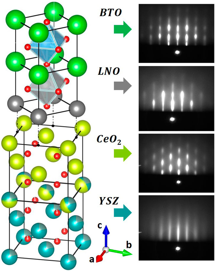
FIGURE 1. Sketch of the fabricated Si(001)/YSZ/CeO2/LaNiO3/BaTiO3 heterostructure, displaying the epitaxial relations. On the right are displayed the corresponding RHEED patterns, obtained after the finalisation of the growth of each layer.
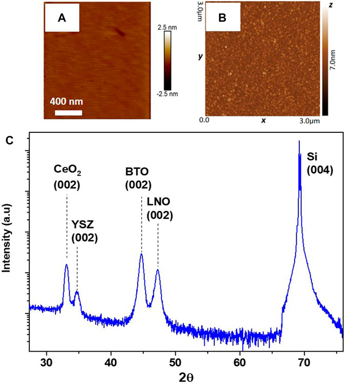
FIGURE 2. (A) Atomic force microscopy topography measured on a Si(001)/YSZ/CeO2/LaNiO3 structure; (B) Atomic force microscopy topography measured on a Si(001)/YSZ/CeO2/LaNiO3/BaTiO3 heterostructure; (C) Bragg–Brentano X-ray diffraction pattern corresponding to a Si(001)/YSZ/CeO2/LaNiO3/BaTiO3 heterostructure. LaNiO3 and BaTiO3 are labelled as LNO and BTO, respectively.
Figure 2C shows a Bragg-Brentano X-ray spectrum corresponding to the Si(001)/YSZ/CeO2/LaNiO3/BaTiO3 heterostructure. Is found the sole presence of (002) peaks of YSZ, CeO2, LaNiO3 and BaTiO3, as expected for an epitaxial heterostructure. The out-of-plane parameters (labelled as c) of the different layers have been extracted from the X-ray scan. YSZ displays an out-of-plane parameter c = 0.516 (1) nm, which is larger as the one corresponding to the bulk compound (0.512 nm). This suggests the presence of in-plane compressive strain, which is at odds with the tensile strain expected from the comparison of the bulk structures but is consistent with previously reported GPA on similar systems Carrero et al. (2020). The presence of compressive strain on YSZ can be related to the formation of a thin SiOx layer (≈3 nm, observable by high resolution STEM-HAADF images) at the Si/YSZ interface upon cooling from the deposition temperature down to room temperature Carrero et al. (2020). CeO2 presents an out-of-plane parameter c = 0.543 (1) nm, which is slightly larger to the one corresponding to the bulk compound (0.541 nm). This is consistent with the expected in-plane compressive strain given the negative lattice mismatch between YSZ and CeO2 bulk structures. LaNiO3 displays an out-of-plane parameter c = 0.383 (1) nm, which is very close to the one of the bulk compound (c = 0.384), reflecting the low mismatch existing between LaNiO3 and CeO2 which leads to a fairly cubic perovskite unit cell Rubi et al. (2002). Finally, the out-of-plane parameter of BaTiO3 is c = 0.406 (1) nm, which is larger than the bulk one (0.403 nm) and is consistent with the negative mismatch existing between LaNiO3 and BaTiO3.
Figure 3A displays a low magnification STEM-HAADF cross-section, where the substrate and the four layers can be visualized. All layers present a uniform thickness (21 nm, 13 nm, 14 nm and 165 nm for YSZ, CeO2, LaNiO3 and BaTiO3, respectively) and the interfaces are sharp. The STEM-HAADF analysis of the buffer layers (YSZ and CeO2) has been already reported by some of the authors of this manuscript in Carrero et al. (2020). Both perovskite layers in our heterostructure display a columnar growth. Figure 3B displays a high magnification STEM-HAADF cross-section of the BaTiO3 layer. Different zones can be observed: while the upper-left squared zone evidences the presence of a high quality, defect free, perovskite structure, the central zone of the image (with darker contrast) shows the presence of a dislocation that transforms a Ba column into a Ti column. Figure 3C–E display GPA analysis performed on CeO2, LaNiO3 and BaTiO3 layers. Colour maps in panels d) and e) show the strain distributions for both in-plane (Exx) and out-of-plane (Eyy) directions, calculated from the STEM-HAADF image of panel c). The GPA analysis was performed taken the BaTiO3 structure as reference. The maps show that the BaTiO3 layer is not fully strained by the LaNiO3 layer, as the latter displays an in-plane compressed lattice (≈-10%) with respect to the former. The presence of defects in the BaTiO3 layer can be observed in the Eyy map, which displays blue-coloured zones were BaTiO3 is locally strained. Figure 4A shows EDS line scans performed on the Si(001)/YSZ/CeO2/LaNiO3/BaTiO3 heterostructure, together with the corresponding chemical quantifications. YSZ, CeO2 and BaTiO3 layers displayed a stochiometry consistent with the nominal one, while some Ni-deficiency was found for the LaNiO3 layer.
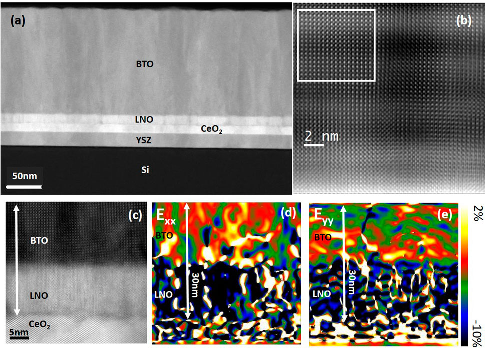
FIGURE 3. (A) Low magnification STEM-HAADF cross-section corresponding to a Si(001)/YSZ/CeO2/LaNiO3/BaTiO3 heterostructure. LaNiO3 and BaTiO3 are labelled as LNO and BTO, respectively; (B) For the same sample, high resolution STEM-HAADF image of the BaTiO3 layer; (C–E) In-plane (Exx) and out-of-plane (Eyy) GPA strain maps corresponding to the LaNiO3 and BaTiO3 layers. See the main text for details.
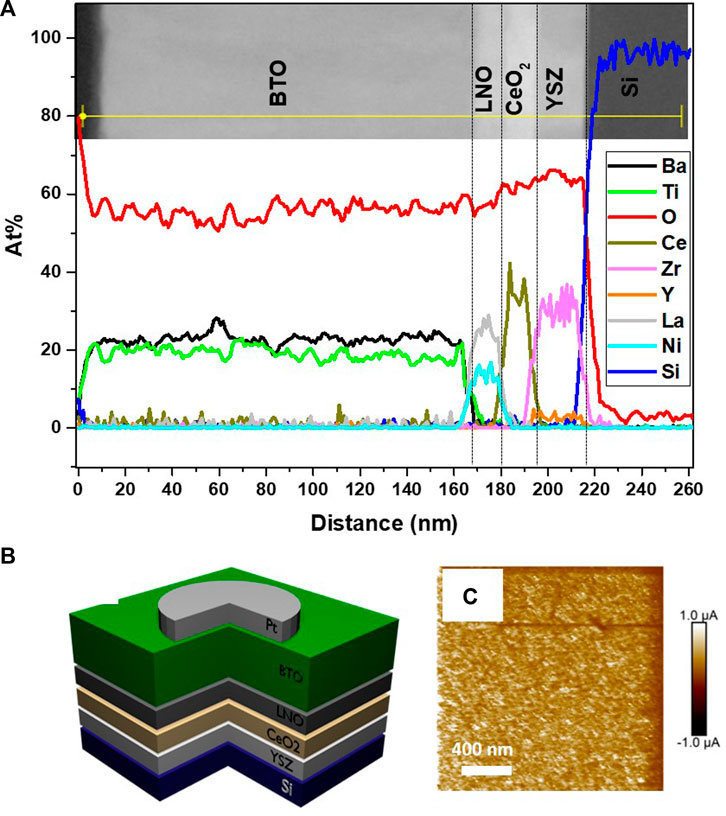
FIGURE 4. (A) Chemical quantification performed on a Si(001)/YSZ/CeO2/LaNiO3/BaTiO3 heterostructure from a STEM-EDS line scan. LaNiO3 and BaTiO3 are labelled as LNO and BTO, respectively; (B) Sketch displaying the final device, used for the electrical characterization. LNO and Pt are the bottom and top electrodes, respectively; (C) Conducting atomic force microscopy map recorded on a Si(001)/YSZ/CeO2/LaNiO3 structure.
3.2 Electrical characterization
A sketch of the device used for the electrical characterization is displayed in Figure 4B. The bottom LaNiO3 electrode was grounded and the electrical stimuli was applied to the top Pt electrode. CAFM experiments were performed on a Si(001)/YSZ/CeO2/LaNiO3 heterostructure (Figure 4C), by applying a 0.25 V DC bias. The measured current values -up to ≈ 1 μA-reflect a high conductivity for a perovskite oxide (Sirena et al. (2010)); in addition, the current distribution displays high spatial uniformity. This confirms that our epitaxial LaNiO3 layer -grown on buffered Si- is an appropriate bottom electrode for our final device, in contrast with the more insulating transport properties observed in polycrystalline LaNiO3 thin films grown directly on Si (Qiao and Bi (2008)). We also notice that the Ni-deficiency we observed in our LaNiO3 layer is not detrimental to its high conductivity, in agreement with previous reports (Wakiya et al. (2002)).
The ferroeletric character of the BaTiO3 layer was tested with different experiments. Figure 5A displays a capacitance-electric field (C-E) curve. The capacitance was acquired with the LCR-meter by assuming a parallel RC circuit, as it is the standard for low-leakage capacitors. An AC excitation voltage with amplitude 0.5 V and a frequency of 10 kHz was used. The C-E curves displays an hysteretic, butterfly-like shaped evolution, typical of ferroelectric devices. From capacitance measurements, we have extracted the BaTiO3 dielectric permittivity, obtaining values ranging between ≈ 400 at low frequencies (100 Hz) to ≈ 170 at higher frequencies (10 kHz), in good agreement with previous reports (Thomas et al. (1999)). Figure 5B displays the current-electric field curve obtained with the Positive-Up Negative-Down (PUND) protocol (a 1 kHz frequency was used), where the presence of ferroelectric displacement peaks are clearly seen. The same figure displays the polarization-electrical field (P-E) loop obtained after the time integration of the current. The P-E loop resembles the one of a standard ferroelectric, despite presenting some asymmetry. This might indicate the existence of an unstable upward polarization (obtained by negatively poling the top electrode), originated by the presence of a downward internal field due to the asymmetry between both electrodes (Lee et al. (1998); Zhou et al. (2019)). However, this should be accompanied by strong (negative) imprints of both C-V and P-E loops [Lee et al. (1998); Zhou et al. (2019)], which do not seem to be present in Figures 5A,B. Therefore, the asymmetry in the P-E loop should be attributed to other effect, such as the presence of asymmetrical leakage currents Noguchi et al. (2019) which were not fully eliminated during the PUND procedure. Values for the remanent polarization PR ≈ 1.3 μC/cm2 and coercive field EC ≈ 120 kV/cm are extracted. Finally, the ferroelectric character of the BaTiO3 layer was confirmed by PFM microscopy, as displayed in the inset of Figure 5A. For this experiment, the polarization of two rectangular zones were written with up and down directions (±8 V), and the PFM image was recorded afterwards. A clear phase contrast is observed, indicating the anti-parallel polarization directions between both zones. The contrast between both zones was found to decrease in a time scale of ≈ 1 h, indicating the presence of depolarization effects.
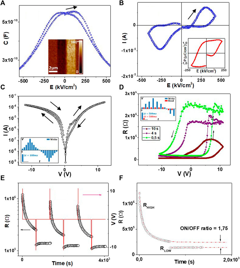
FIGURE 5. (A) Capacitance-electric field (C–E) curve recorded on a Si(001)/YSZ/CeO2/LaNiO3/BaTiO3/Pt device. The inset displays a PFM microscopy phase image, recorded after writing two rectangles with up and down polarization; (B) Current-electric field (obtained by using the PUND protocol, main panel) and polarization-electric field (P-E, inset) curves measured on the same device; (C) Dynamic current-voltage curve recorded on the same device. The presence of hysteresis reflects the existence of memristive behavior. The inset shows the stimulation protocol; (D) Remanent vs. writing voltage loops for the same device, measured for different time-separation between consecutive write pulses. The inset shows the stimulation protocol. See main text for further details; (E) Resistance relaxations measured after the application of single (positive and negative) voltage pulses. We recall the semi-log scale of the plot; (F) Resistance relaxations and exponential fittings for RHIGH and RLOW states, displayed in linear scale. The existence of a mixture of volatile and non-volatile memristive effects is seen.
We turn now to the memristive properties. Figure 5C shows a dynamic current-voltage (I-V) curve recorded on a LaNiO3/BaTiO3/Pt device. The stimulation protocol is displayed in the inset, and consisted on a pulsed ramp of DC voltage pulses, in the range +12 V/-12 V with a step of 0.2 V and a time-width for each pulse of 100 m. The delay time between consecutive pulses was 0.5 s. The current is measured during the application of each pulse. The I-V curve displays an hysteretic behavior, which is the signature of memristive effects. With positive voltage, the system goes from a low resistance state (LR, higher current) to a high resistance state (HR, lower current), in what is usually called the RESET process. The inverse resistance transition is found for negative voltage (SET process). An ON-OFF ratio of ≈ 10.4 was extracted at 1 V. In order to track the evolution of the remanent resistance as a function of the writing voltage (usually known as Hysteresis Switching Loop, HSL [Rozenberg et al. (2010); Rubi et al. (2013)]), small reading voltages (with amplitude of few hundreds of mV) are usually applied in between writing pulses and the current is recorded in order to extract the remanent resistance of the device without changing it. Given the high remanent resistance values of the device
3.3 Working model and discussion
In order to explain the evolution of the remanent resistance with the writing voltage and time, several ingredients should be taken into account. We notice that BaTiO3 is a n-type semiconductor, with electron affinity Eea ≈ 3.8 eV, which is prone to form Schottky interfaces when placed in contact with high work function (W) metals. In our case, the work functions of Pt and LaNiO3 are W ≈ 5.6 and W ≈ 4.5 eV, respectively (see Figure 6A for a sketch of the corresponding energy band diagrams). For metal-semiconductor contacts, we recall that the height of the interface Schottky barrier Φ0 is usually estimated as Φ0 = W - Eea. In our case, it is therefore expected that a significantly higher Schottky barrier will be formed at the BaTiO3/Pt interface with respect to the BaTiO3/LaNiO3 interface (Φ0 ≈ 1.8 eV and 0.7 eV, respectively, see the sketch of Figure 6B). As it is the case of many asymmetric memristive devices driven by interface mechanisms (Rozenberg et al. (2010)), the BaTiO3/Pt barrier, displaying the highest height, will dominate the electrical transport and the memristive effect.
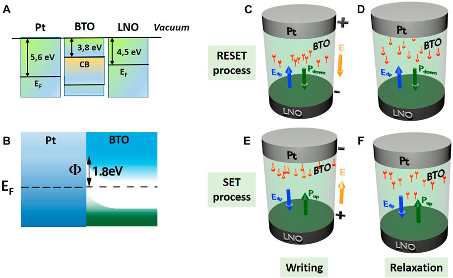
FIGURE 6. (A) Sketch with a comparison of the main features of the band structures of Pt, BaTiO3 (BTO) and LaNiO3 (LNO). The work functions of the metals and the electron affinity of BaTiO3 (all in eV) are indicated. EF and CB refer to the metals Fermi levels and the bottom of the BTO conduction band, respectively; (B) Band diagram corresponding to the Schottky Pt/BaTiO3 interface. The barrier height Φ ≈1.8 eV is indicated; (C–F) Sketch depicting the memristive mechanism of our Si(001)/YSZ/CeO2/LaNiO3/BaTiO3/Pt devices. The top row illustrates the RESET process during the application of the external voltage (C) and the resistance relaxation in zero bias afterwards (D). The directions of the external electrical field, the ferroelectric polarization and the depolarizing field are indicated with yellow, green and blue arrows, respectively. Oxygen vacancies are depicted as orange balls. The bottom row illustrates the SET process, both during the application of the external voltage (E) and the relaxation afterwards (F).
Upon electrical cycling, the memristive behavior is related to the modulation of the BaTiO3/Pt interface resistance by different effects. In the first place, we have the influence of the direction of the electrical polarization on the barrier height (Rault et al. (2013); Hubmann et al. (2016); Pintilie et al. (2007); Farokhipoor and Noheda (2014); Liu et al. (2013). A polarization pointing to the barrier decreases its height according to Φ ≈ Φ0 - γ|P|, where |P| is the polarizarion absolute value and γ is a constant [see Ferreyra et al. (2020a) and references therein]. This lowers the interface resistance. The inverse effect is found for the opposite polarization direction (Φ ≈ Φ0 + γ|P|). In the second place, we should consider the effect of OV dynamics on the interface resistance. We recall that OV dynamics drives the memristive effect occurring at the interface of several oxide/metal systems Rozenberg et al. (2010); Ferreyra et al. (2019; 2020b). OV are known to locally decrease the resistivity of BaTiO3 Yang et al. (2004). These vacancies are charged and they can migrate due to the action of electrical fields. This field might come either from the application of external voltage or from the ferroelectric depolarizing field EDP, arising from an incomplete screening by the metallic electrodes of the ferroelectric bound charges. The latter introduces a coupling between the ferroelectric polarization and OV dynamics, as we have previously discussed and modelled for symmetric Pt/PZT/Pt and SrRuO3/BaTiO3/SrRuO3 devices Ferreyra et al. (2020a), that accounts for resistance relaxations under zero external bias. We recall that the strongest electric field exists close to the BaTiO3/Pt interface, which is a consequence of its highly resistive nature due to the presence of the highest energy barrier among the two interfaces Ghenzi et al. (2010).
Bearing in mind the previous considerations, the observed phenomenology found in our asymmetric LaNiO3/BaTiO3/Pt can be explained as follows (see the sketch displayed in Figures 6C–E). As we have mentioned, the memristive effect is localized at the BaTiO3/Pt interface, displaying a high Schottky barrier. When a positive voltage is applied (Figure 6C), the resistance increases because of the synergistic contribution of the Schottky barrier increase due to the downward switching of the polarization and the removal -by the external electrical field-of OV from the interface to deeper zones of the BaTiO3 layer. When the external voltage is removed (Figure 6D), some of these OV are re-injected at the BaTiO3/Pt interface by the action of EDP -pointing upwards, opposite to the polarization direction-which progressively relaxes the resistance to lower values. As with this polarization direction the Schottky barrier is in its highest value, so is the local electrical field acting on the BaTiO3/Pt interface and the relaxations are therefore significant. When a negative voltage is applied to the device (Figure 6E), the resistance decreases as the barrier height decreases with the upward switching of the polarization direction and the injection of OV into the interface, under the action of the external field. After the electrical stimulation is removed (Figure 6F), some OV will migrate-driven by a downward EDP- from the interface to the deeper zone of the BaTiO3 layer, producing an increase of the resistance with time. However, as in this situation the polarization points to the interface and this lowers the height of the Schottky barrier, the local electrical field acting at the interface will be milder than in the case with inverse polarization and this explains the more subtle resistance relaxations and the asymmetry found in the resistance relaxations after RESET and SET events.
We recall that Qian et al. (2019) found that two different mechanisms contribute to the electroresistance of BaTiO3-based ferroelectric memristors. The presence of one or the other mechanism was the time length of the writing pulses. For short pulses (20 μs) the memristive behavior was dominated by the modulation of the Schottky barrier by the direction of the ferroelectric polarization. For longer pulses (20 s) oxygen vacancy electromigration dominated the change of the Schottky barrier resistance. Our writing pulses present a time-width of 100 ms and are therefore in between the time-widths explored by Qian et al. It is therefore natural to propose, in our case, a coexistence (and competition) between both mechanisms, as was already discussed.
We also notice that our working model assumed that no polarization decay occurs in the time-scale involved in the electrical measurements. This might be concluded from the fact that the observed resistance relaxations present characteristic times of a few minutes, which are significantly faster than the depolarization effects infered from PFM measurements (typical times ≈ 1 h). However, we notice that the BaTiO3 boundary conditions (given by the presence or not of Pt top electrode) are different in both experiments, so different depolarizing times might be involved. This suggests that a depolarization effect could be also present in the observed resistance relaxations, an issue that needs to be addressed in the future.
Another possible mechanism that might account for the existence of resistance relaxations in zero external bias is OV back-diffusion Baeumer et al. (2015). This requires the existence of strong OV gradients as those found in systems with memristive mechanisms based on the completion/disruption of OV nanofilaments; for instance Zhang et al. reported OV densities going from 1 × 10¹⁹m−3 for pristine hafnia to 1 × 1026 m−3 at the center of an OV filament (Zhang et al. (2022)). This scenario can be disregarded in our case as the I-V curve of Figure 5C and the remanent resistance loop of Figure 5D display opposite chiralities to those expected for a filamentary memristive mechanism. Our system displays, instead, an interface-type memristive effect, where OV density profiles present significantly milder gradients Román Acevedo et al. (2018); Ferreyra et al. (2020a). Based on these arguments, we consider that resistance relaxations due to OV back-diffusion are unlikely in our case.
We finally mention that volatile memristive effects driven by the depolarizing field-driven oxygen vacancy dynamics might be mastered by proper interface engineering. We recall that the depolarizing field comes from the incomplete screening of ferroelectric bound charges by the metallic electrodes. The screening capability of the electrode can be controlled by changing the fabrication conditions (for example, its conductivity can be fine-tuned by the deposition and annealing temperature) or by the quality of the interface (i.e. the presence of epitaxy, roughness, interdiffusion). Also, EDP might be tuned by placing ultra-thin insulating barriers in between the ferroelectric and the metal (Lichtensteiger et al. (2014)). By using these knobs the characteristics of the resistance relaxations (for example, their time-constant) might be adapted to the final application needs.
4 Conclusion
In this work we have developed epitaxial BaTiO3 ferroelectric memristors integrated with silicon. It was found the presence of coexisting volatile and non-volatile memristive effects, with the presence of strongly asymmetric relaxations after SET and RESET events. This phenomenology arises from the combined effect of the interface barrier modulation of the BaTiO3/Pt interface by the ferroelectric polarization entangled with OV dynamics, the latter driven by the depolarizing field. The results reported here might be relevant for the development of neuromorphic hardware as our devices can electrically replicate, in the same unit, the behavior of neurons and synapses. Their volatile memristive properties can be useful for the development of applications such as true random generators, selectors in cross-bar arrays, physical unclonable functions and also in reservoir computing (Wang et al. (2020)). Finally, we notice that the integrability of our devices with silicon is of paramount importance to take advantage of existing micro and nanoelectronics technology.
Data availability statement
The raw data supporting the conclusion of this article will be made available by the authors, without undue reservation.
Author contributions
MR fabricated the samples and performed the structural and electrical characterization. MA performed the STEM experiments and GPA analysis. MS conducted the CAFM tests. UL provided the PLD targets. DR conceived the experiments, did the general coordination and supervision of the work and wrote the manuscript.
Acknowledgments
We acknowledge Marten Piantek, from LMA-INA-UNIZAR, for the PFM measurements. We acknowledge support from ANPCyT (PICT 2019-02781, PICT2020A-00415) and EU-H2020-RISE project MELON (Grant No. 872631).
Conflict of interest
The authors declare that the research was conducted in the absence of any commercial or financial relationships that could be construed as a potential conflict of interest.
Publisher’s note
All claims expressed in this article are solely those of the authors and do not necessarily represent those of their affiliated organizations, or those of the publisher, the editors and the reviewers. Any product that may be evaluated in this article, or claim that may be made by its manufacturer, is not guaranteed or endorsed by the publisher.
References
Baeumer, C., Schmitz, C., Ramadan, A. H. H., Du, H., Skaja, K., Feyer, V., et al. (2015). Spectromicroscopic insights for rational design of redox-based memristive devices. Nat. Commun. 6, 8610. doi:10.1038/ncomms9610
Blom, P. W. M., Wolf, R. M., Cillessen, J. F. M., and Krijn, M. P. C. M. (1994). Ferroelectric Schottky diode. Phys. Rev. Lett. 73, 2107–2110. doi:10.1103/physrevlett.73.2107
Carrero, A., Roman, A., Aguirre, M., and Steren, L. B. (2020). Nanoscale structural characterization of manganite thin films integrated to silicon correlated with their magnetic and electric properties. Thin Solid Films 709, 138189. doi:10.1016/j.tsf.2020.138189
Chanthbouala, A., Garcia, V., Cherifi, R. O., Bouzehouane, K., Fusil, S., Moya, X., et al. (2012). A ferroelectric memristor. Nat. Mat. 11, 860–864. doi:10.1038/nmat3415
Farokhipoor, S., and Noheda, B. (2014). Screening effects in ferroelectric resistive switching of BiFeO3 thin films. Apl. Mat. 2, 056102. doi:10.1063/1.4875355
Ferreyra, C., Acevedo, W. R., Gay, R., Rubi, D., and Sánchez, M. J. (2019). Oxygen vacancy dynamics in redox-based interfaces: Tailoring the memristive response. J. Phys. D. Appl. Phys. 53, 015302. doi:10.1088/1361-6463/ab46d3
Ferreyra, C., Rengifo, M., Sánchez, M., Everhardt, A., Noheda, B., and Rubi, D. (2020a). Key role of oxygen-vacancy electromigration in the memristive response of ferroelectric devices. Phys. Rev. Appl. 14, 044045. doi:10.1103/physrevapplied.14.044045
Ferreyra, C., Sánchez, M., Aguirre, M., Acha, C., Bengió, S., Lecourt, J., et al. (2020b). Selective activation of memristive interfaces in TaOx-based devices by controlling oxygen vacancies dynamics at the nanoscale. Nanotechnology 31, 155204. doi:10.1088/1361-6528/ab6476
Garcia, V., Fusil, S., Bouzehouane, K., Enouz-Vedrenne, S., Mathur, N. D., Barthelemy, A., et al. (2009). Giant tunnel electroresistance for non-destructive readout of ferroelectric states. Nature 460, 81–84. doi:10.1038/nature08128
Ghenzi, N., Sánchez, M. J., Gomez-Marlasca, F., Levy, P., and Rozenberg, M. J. (2010). Hysteresis switching loops in ag-manganite memristive interfaces. J. Appl. Phys. 107, 093719. doi:10.1063/1.3372617
Hubmann, A. H., Li, S., Zhukov, S., von Seggern, H., and Klein, A. (2016). Polarisation dependence of Schottky barrier heights at ferroelectric BaTiO3/RuO2 interfaces: Influence of substrate orientation and quality. J. Phys. D. Appl. Phys. 49, 295304. doi:10.1088/0022-3727/49/29/295304
Ielmini, D., and Waser, R. (2016). Resistive switching: From fundamentals of nanoionic redox processes to memristive device applications. Weinheim, Germany: Wiley VCH.
Kumar, S., Wang, X., Strachan, J., Yang, Y., and Lu, W. (2022). Dynamical memristors for higher-complexity neuromorphic computing. Nat. Rev. Mat. 7, 575–591. doi:10.1038/s41578-022-00434-z
Lee, J., Choi, C. H., Park, B. H., Noh, T. W., and Lee, J. K. (1998). Built-in voltages and asymmetric polarization switching in Pb(Zr, Ti)O3 thin film capacitors. Appl. Phys. Lett. 72, 3380–3382. doi:10.1063/1.121610
Lichtensteiger, C., Fernandez-Pena, S., Weymann, C., Zubko, P., and Triscone, J.-M. (2014). Tuning of the depolarization field and nanodomain structure in ferroelectric thin films. Nano Lett. 14, 4205–4211. doi:10.1021/nl404734z
Liu, X., Wang, Y., Burton, J. D., and Tsymbal, E. Y. (2013). Polarization-controlled ohmic to Schottky transition at a metal/ferroelectric interface. Phys. Rev. B 88, 165139. doi:10.1103/physrevb.88.165139
Lubig, A., Buchal, C., Guggi, D., Jia, C., and Stritzker, B. (1992). Epitaxial growth of monoclinic and cubic ZrO2 on Si(100) without prior removal of the native SiO2. Thin Solid Films 217, 125–128. doi:10.1016/0040-6090(92)90617-k
Lyu, J., Fina, I., Solanas, R., Fontcuberta, J., and Sánchez, F. (2018). Tailoring lattice strain and ferroelectric polarization of epitaxial BaTiO3 thin films on Si(001). Sci. Rep. 8, 495. doi:10.1038/s41598-017-18842-5
Mehonic, A., and Kenyon, A. (2022). Brain-inspired computing needs a master plan. Nature 604, 255–260. doi:10.1038/s41586-021-04362-w
Meyer, R., and Waser, R. (2006). Hysteretic resistance concepts in ferroelectric thin films. J. Appl. Phys. 100, 051611. doi:10.1063/1.2337078
Noguchi, Y., Matsuo1, H., Kitanaka, Y., and Miyayama, M. (2019). Ferroelectrics with a controlled oxygen-vacancy distribution by design. Sci. Rep. 9, 4225. doi:10.1038/s41598-019-40717-0
Pintilie, L., Stancu, V., Trupina, L., and Pintilie, I. (2010). Ferroelectric Schottky diode behavior from a SrRuO3-Pb(Z r0.2Ti0.8)O3-Ta structure. Phys. Rev. B 82, 085319. doi:10.1103/physrevb.82.085319
Pintilie, L., Vrejoiu, I., Hesse, D., LeRhun, G., and Alexe, M. (2007). Ferroelectric polarization-leakage current relation in high quality epitaxial Pb(Zr, Ti)O3 films. Phys. Rev. B 75, 104103. doi:10.1103/physrevb.75.104103
Qian, M., Fina, I., Sulzbach, M. C., Sánchez, F., and Fontcuberta, J. (2019). Synergetic electronic and ionic contributions to electroresistance in ferroelectric capacitors. Adv. Electron. Mat. 5, 1800646. doi:10.1002/aelm.201800646
Qiao, L., and Bi, X. F. (2008). Strain state, microstructure and electrical transport properties of LaNiO3 films grown on si substrates. J. Phys. D. Appl. Phys. 41, 195407. doi:10.1088/0022-3727/41/19/195407
Rault, J. E., Agnus, G., Maroutian, T., Pillard, V., Lecoeur, P., Niu, G., et al. (2013). Interface electronic structure in a metal/ferroelectric heterostructure under applied bias. Phys. Rev. B 87, 155146. doi:10.1103/physrevb.87.155146
Román Acevedo, W., Ferreyra, C., Sánchez, M. J., Acha, C., Gay, R., and Rubi, D. (2018). Concurrent ionic migration and electronic effects at the memristive TiOx/La1/3Ca2/3 MnO3−x interface. J. Phys. D. Appl. Phys. 51, 125304.
Román, A., Rengifo, M., Saleh Medina, L., Reinoso, M., Negri, R., Steren, L., et al. (2017). BaTiO3 thin films on platinized silicon: Growth, characterization and resistive memory behavior. Thin Solid Films 628, 208–213. doi:10.1016/j.tsf.2017.03.038
Rozenberg, M. J., Sánchez, M. J., Weht, R., Acha, C., Gomez-Marlasca, F., and Levy, P. (2010). Mechanism for bipolar resistive switching in transition-metal oxides. Phys. Rev. B 81, 115101. doi:10.1103/physrevb.81.115101
Rubi, D., Duhalde, S., Terzzoli, M., Leyva, G., Polla, G., Levy, P., et al. (2002). Structural and electrical characterisation of La0.5Ca0.5MnO3 thin films grown by pulsed laser deposition. Phys. B Condens. Matter 320, 86–89. doi:10.1016/s0921-4526(02)00649-x
Rubi, D., Gomez-Marlasca, F., Bonville, P., Colson, D., and Levy, P. (2012). Resistive switching in ceramic multiferroic Bi0.9Ca0.1FeO3. Phys. B Condens. Matter 407, 3144–3146. doi:10.1016/j.physb.2011.12.048
Rubi, D., Tesler, F., Alposta, I., Kalstein, A., Ghenzi, N., Gomez-Marlasca, F., et al. (2013). Two resistive switching regimes in thin film manganite memory devices on silicon. Appl. Phys. Lett. 103, 163506. doi:10.1063/1.4826484
Sawa, A. (2008). Resistive switching in transition metal oxides. Mater. Today 11, 28–36. doi:10.1016/s1369-7021(08)70119-6
Scigaj, M., Chao, C. H., Gázquez, J., Fina, I., Moalla, R., Saint-Girons, G., et al. (2016). High ferroelectric polarization in c-oriented BaTiO3 epitaxial thin films on SrTiO3/Si(001). Appl. Phys. Lett. 109, 122903. doi:10.1063/1.4962836
Scigaj, M., Dix, N., Fina, I., Bachelet, R., Warot-Fonrose, B., Fontcuberta, J., et al. (2013). Ultra-flat BaTiO3 epitaxial films on Si(001) with large out-of-plane polarization. Appl. Phys. Lett. 102, 112905. doi:10.1063/1.4798246
Sirena, M., Zimmers, A., Haberkorn, N., Kaul, E. E., Steren, L. B., Lesueur, J., et al. (2010). Influence of ion implantation on the magnetic and transport properties of manganite films. Phys. Rev. B 81, 134439. doi:10.1103/physrevb.81.134439
Thomas, R., Dube, D., Kamalasanan, M., and Chandra, S. (1999). Optical and electrical properties of BaTiO3 thin films prepared by chemical solution deposition. Thin Solid Films 346, 212–225. doi:10.1016/s0040-6090(98)01772-6
Tian, J., Tan, Z., Fan, Z., Zheng, D., Wang, Y., Chen, Z., et al. (2019). Depolarization-field-induced retention loss in ferroelectric diodes. Phys. Rev. Appl. 11, 024058. doi:10.1103/physrevapplied.11.024058
Tsymbal, E. Y., and Kohlstedt, H. (2006). Tunneling across a ferroelectric. Science 313, 181–183. doi:10.1126/science.1126230
Wakiya, N., Azuma, T., Shinozaki, K., and Mizutani, N. (2002). Low-temperature epitaxial growth of conductive LaNiO3 thin films by rf magnetron sputtering. Thin Solid Films 410, 114–120. doi:10.1016/s0040-6090(02)00238-9
Wang, R., Yang, J.-Q., Mao, J.-Y., Wang, Z.-P., Wu, S., Zhou, M., et al. (2020). Recent advances of volatile memristors: Devices, mechanisms, and applications. Adv. Intell. Syst. 2, 2000055. doi:10.1002/aisy.202000055
Weber, M. C., Guennou, M., Dix, N., Pesquera, D., Sánchez, F., Herranz, G., et al. (2016). Multiple strain-induced phase transitions in LaNio3 thin films. Phys. Rev. B 94, 014118. doi:10.1103/physrevb.94.014118
Yang, G. Y., Dickey, E. C., Randall, C. A., Barber, D. E., Pinceloup, P., Henderson, M. A., et al. (2004). Oxygen nonstoichiometry and dielectric evolution of BaTiO3. Part I—improvement of insulation resistance with reoxidation. J. Appl. Phys. 96, 7492–7499. doi:10.1063/1.1809267
Yin, K., Li, M., Liu, Y., He, C., Zhuge, F., Chen, B., et al. (2010). Resistance switching in polycrystalline BiFeO3 thin films. Appl. Phys. Lett. 97, 042101. doi:10.1063/1.3467838
Yu, S. (2017). Neuro-inspiring computing using resistive synaptic devices. New York, United States: Springer International Publishing.
Zhang, K., Ren, Y., Ganesh, P., and Cao, Y. (2022). Effect of electrode and oxide properties on the filament kinetics during electroforming in metal-oxide-based memories. npj Comput. Mat. 8, 76. doi:10.1038/s41524-022-00770-2
Zhou, Y., Wang, C., Lou, X., Tian, S., Yao, X., Ge, C., et al. (2019). Internal electric field and polarization backswitching induced by nb doping in BiFeO3 thin films. ACS Appl. Electron. Mat. 1, 2701–2707. doi:10.1021/acsaelm.9b00737
Keywords: memristors, neuromorphic computing, ferroelectrics, perovskites, integration with silicon
Citation: Rengifo M, Aguirre MH, Sirena M, Lüders U and Rubi D (2022) Epitaxial ferroelectric memristors integrated with silicon. Front. Nanotechnol. 4:1092177. doi: 10.3389/fnano.2022.1092177
Received: 07 November 2022; Accepted: 07 December 2022;
Published: 16 December 2022.
Edited by:
Tamalika Banerjee, University of Groningen, NetherlandsReviewed by:
Ignasi Fina, Institute of Materials Science of Barcelona (CSIC), SpainTakeaki Yajima, Kyushu University, Japan
Regina Dittmann, Julich Research Center (HZ), Germany
Copyright © 2022 Rengifo, Aguirre, Sirena, Lüders and Rubi. This is an open-access article distributed under the terms of the Creative Commons Attribution License (CC BY). The use, distribution or reproduction in other forums is permitted, provided the original author(s) and the copyright owner(s) are credited and that the original publication in this journal is cited, in accordance with accepted academic practice. No use, distribution or reproduction is permitted which does not comply with these terms.
*Correspondence: Diego Rubi, ZGllZ28ucnViaUBnbWFpbC5jb20=