 Malte J. M. J. Becher
 Julia Jagosz2
- 1Applied Laser Technologies, Ruhr University Bochum, Bochum, Germany
- 2Microsystems Technology, Ruhr University Bochum, Bochum, Germany
- 3Laser Center (LFM), University of Applied Sciences Münster, Steinfurt, Germany
The formation of laser-induced periodic surface structures (LIPSSs) on the atomic layer-deposited (ALD) molybdenum disulfide (MoS2) upon femtosecond laser processing is studied experimentally. Laser-processing parameters such as average laser power and the scan speed at which the formation of the periodic nanostructures takes place are identified. Optical and scanning electron microscopy are applied to identify the parameter regions for the different LIPSS formations and transitions between them. High- and low-spatial frequency LIPSS (HSFL and LSFL) with two distinct periods λLSFL ≈ 1.1 μm and λHSFL ≈ 83 nm can be observed. The HSFL are dominating at higher and the LSFL at lower laser average powers. Formation of LIPSS is found to inhibit laser ablation at lower scan speeds.
1 Introduction
Recent growing interest in 2D transition metal dichalcogenide (TMDC) materials such as molybdenum disulfide (MoS2) is driven by a large number of applications such as photo-catalysis, sensing and disinfection (Wang and Mi, 2017), semiconductor electronics (Butler et al., 2013), and energy storage (Acerce et al., 2015). The possibility to modify such thin layers with lasers enables their application for electronic devices (Radisavljevic et al., 2011). Two important types of the MoS2 layer modifications required for all-MoS2 electronic and sensing devices are crystallization (Zhang et al., 2020) and patterning. Structuring of thin MoS2 layers can be conducted by direct laser ablation (Pan et al., 2020), which can be used, e.g., to write periodic stripes with the resolution down to approximately 250 nm (Kim et al., 2016). Such a deterministic way of patterning has certain disadvantages, like slow processing velocity and high requirements for the positioning precision and temperature stability. An alternative way for MoS2 nanopatterning could be self-organization, i.e., appropriate choice of the processing parameters at which the homogeneously deposited layer undergoes some instability, manifesting itself as a periodic pattern. Using this method, self-organized hexagonal patterns were recently observed in MoS2 upon fs laser processing (Becher et al., 2023).
LIPSSs are self-organized structures with periods usually comparable to the wavelength of laser radiation (LSFL — low-spatial frequency LIPSS) or approximately one order of magnitude smaller than the wavelength (HSFL — high-spatial frequency LIPSS) (Bonse et al., 2012). The physical mechanism of the LIPSS formation is still under debate. Most probably the LSFL formation is a multi-step process (Gurevich et al., 2020), starting with the incident wave interfering with the wave scattered by surface roughness (Emmony et al., 1973; Sipe et al., 1983) and periodically modulating the temperature of the electrons in a thin surface layer. Then, the electrons heat up the lattice, whereupon the amplitude of the relative temperature modulation increases (Gurevich et al., 2017). This periodic lattice temperature modulation forms the LIPSS either by selective ablation or by hydrodynamic flow in the melt. The formation mechanisms of the HSFL are less clear and can involve either near-field amplification of the field on the LSFL structure (Geng et al., 2023) or de-wetting of the grooves formed by the LSFL ribbons (Khare et al., 2007). Such patterns were first discovered in germanium (Birnbaum, 1965) and were recently observed in 2D materials, such as graphene (Beltaos et al., 2014; Kasischke et al., 2018). However, to the best of our knowledge, no high- and low-spatial frequency LIPSS have been observed in MoS2 simultaneously, and the corresponding laser processing parameters have not been studied systematically. Recently, formation of HSFL-like structures in MoS2 referred to as nanoribbons was reported by Zuo et al. (2019). Zuo et al. (2019) fabricated large arrays of regularly arranged MoS2 nanowires using the femtosecond laser technique on exfoliated flakes. Based on these nanoribbons, they produced macroscopic FET structures that exhibit rectifying behavior. Salimon et al. (2023) were able to demonstrate significantly improved photo-conductivity and photo-current on 200-nm ribbons fabricated via LIPSS. Furthermore, the nanopatterning of 2D materials improves the performance of switches and sensors (Rahman and Lu, 2022). In addition to the electrotechnical applications, MoS2 is widely used as a lubricant. For example, MoS2 nanocoatings are used in space applications as a solid-based lubricating material (Mukhtar et al., 2023). Nanostructuring using LIPSS could further improve the tribological properties of these coatings (Bonse et al., 2018). In this paper, we demonstrate direct formation of LSFL and HSFL in ALD-deposited MoS2 layers irradiated with femtosecond laser pulses and investigate the parameters at which the LIPSS formation occurs.
2 Materials and methods
2.1 Atomic layer deposition of MoS2
A plasma-enhanced ALD (PE-ALD) process (Sharma et al., 2018; Jagosz et al., 2022) was used to deposit a MoS2 film on a silicon dioxide (d = 200 nm)/silicon substrate. The substrate temperature was Tsub ≈ 230 °C due to limited thermal contact between the substrate and table (T = 300 °C). The MoS2 film was deposited using a SENTECH Instruments GmbH SI ALD reactor equipped with a remote capacitive coupled plasma source (f = 13.56 MHz). The precursor Bis(t-butylimido)bis(dimethylamino)molybdenum (Strem, 98%) was heated in a stainless-steel canister to T = 50 °C. A 100-sccm nitrogen bubbling flow rate was applied to facilitate precursor delivery into the reactor. A plasma mixture of 5 sccm hydrogen sulfide (99.5%) and 45 sccm argon was used as the co-reactant. The plasma was operated at a power of 200 W at a pressure of 10 Pa. After 400 cycles, a 34-nm-thick polycrystalline MoS2 film (verified by ellipsometric measurements) was deposited.
2.2 Generation of LIPSS
A femtosecond laser system from Jenoptik (JenLas D2.fs, λ = 1025 nm ± 10 nm, and τP = 400 fs) with a repetition rate of frep = 200 kHz was used for the processing of the MoS2 samples. The laser power was adjusted by a half—wave plate and a polarization beam splitter. The laser beam is led to a galvanometer scanner and focused on the sample surface with an F-Θ lens, with a spot size of d ≥ 27 μm. Rectangular areas (250 μm × 250 μm) were processed by scanning the spot with a line distance of 5 μm.
2.3 Characterization
Optical micrograph images were captured with a camera [mvBlueFOX-ML/IGC, (Matrix Vision GmbH)] in combination with a ×100 NA 0.85 objective. Scanning electron microscope (SEM) images were captured with a Schottky field emission electron microscope Leo Gemini 982 at 2 kV.
3 Results and discussion
For the generation of LIPSS, square areas of 250 μm × 250 μm were processed on the MoS2 film. Depending on the chosen parameters, seven different topographies could be determined in the processed areas. Starting at PL = 20 mW and vscan = 0.1 mm/s, an unstable generation of LIPSS appears. With the increasing laser power (PL < 50 mW) and scan speed (vscan < 100 mm/s) stable, areal LIPSS starts to form. Further increase of the laser power results in modification of the film without formation of LSFL, while further increase of the scan speed still results in a formation of LSFL, but MoS2 starts to get ablated. A possible explanation of the latter effect will be given at the end of this section. Figure 1 gives an overview about the different regions, depending on the laser power and scan speed.
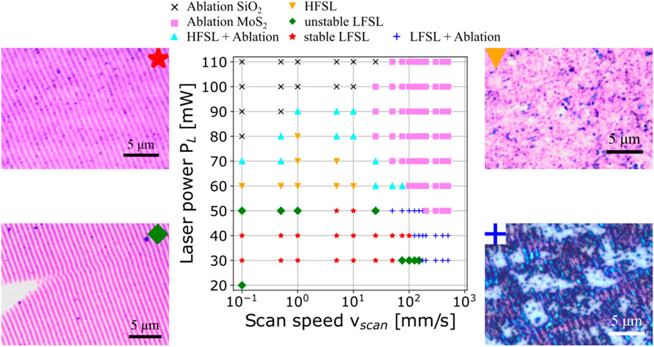
FIGURE 1. Overview of the generated MoS2 surface, depending on the laser power and the scan speed. The first appearance of unstable LIPSS (green rectangles) is visible at PL = 20 mW and vscan = 0.1 mm/s. With higher laser powers and scan speeds, a region is formed, where stable and areal LIPSS are generated (red stars). By increasing only the scan speed, partial ablation of the MoS2 film and the LIPSS is induced (blue crosses). At lower scan speeds but higher laser powers, the formation of LIPSS disappears in the optical micrograph and a different modification of the MoS2 film appears (orange triangles).
A more detailed view of the MoS2 LIPSS is shown in Figure 2. Here, a processed area (PL = 40 mW and vscan = 0.5 mm/s) is displayed, with different magnifications. Figure 2A shows a continuous pattern of LSFL with a period of Λ ≈ 1.1 μm, which is close to the laser wavelength of λ = 1.03 μm. Upon closer examination at higher magnifications (Figure 2B,C), it becomes apparent that the HSFL also forms in an orthogonal pattern to the LSFL. The period of the HSFL is around Λ = 83nm. These “nanoribbons” were described by Zuo et al. (2019) in the past but without the appearance of LSFL. Figure 3 demonstrates the transition between the appearance of LSFL and HSFL, by adjusting the laser power at a constant scan speed (PL = 30–90 mW and vscan = 0.5 mm/s). Processing the MoS2 film with low laser powers (PL = 30 mW), an LSFL pattern forms, whose stripes consist of the HSFL pattern (seen in Figures 2, 3A). With the rise of the laser power above PL = 50 mW, the LSFL pattern fades away and only the HSFL patterns are formed. Figures 3B,C show that the degree of ablation and a resulting covering of the MoS2 HSFL can be adjusted, based on the laser power. More SEM images of the laser power-depending generation of HSFL and LSFL can be found in Supplementary Figure S1.
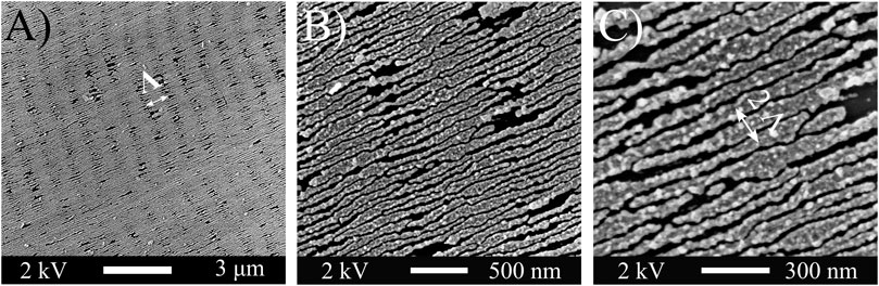
FIGURE 2. SEM images of LIPSS generated with PL = 40 mW and vscan = 0.5 mm/s with (A) 10.000x, (B) 50.000x, and (C) 100.000x magnification. In (A) and (B), the LSFL are seen, with a period of approximated Λ ≈ 1.1 μm. Images (B) and (C) show that the LSFL consists of HSFL with a period of approximate Λ ≈ 83 nm.
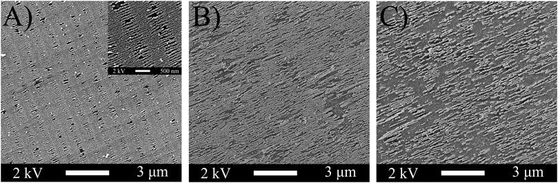
FIGURE 3. SEM images of the evolution of HSFL and LSFL depending on the average laser power with a constant scan velocity vscan = 0.5 mm/s. (A) With a laser power of PL = 30 mW, both HSFL and LSFL start to build up. The inset image (50.000x magnification) shows that the LSFL consists of HSFL with different thicknesses. (B) When the laser power is risen to PL = 60 mW, no LSFL is built and only the HSFL is formed in the MoS2 film. (C) An even further rise of the laser power to PL = 90 mW leads to partial ablation of the MoS2 HSFL, resulting in a more island-like HSFL appearance.
The reason why the HSFL dominates at higher laser power is not fully understood but can be linked to the theory of LIPSS formation. The commonly used theory suggests that the periodic pattern appears due to interference between the incident and the surface-scattered waves (Emmony et al., 1973; Sipe et al., 1983). In the later steps of this multi-step formation process (Gurevich et al., 2020), the interference between these waves modulates first the electron and then the lattice temperatures, and causes surface modification. This is shown in Figure 3A, in which two perpendicular periodic patterns can be seen: a modified (as HSFL) MoS2 film in the nodes and an unmodified MoS2 film in the anti-nodes of the temperature profile. Why the modified MoS2 layer transforms to HSFL is not clear and out of scope of this paper. However, as the laser power and the pulse energy increase, the amplitude of the field in the anti-nodes grows and the area at which the HSFL formation is reduced grows too. This leads to an increased area with thinner HSFL and a decreased area with thicker HSFL-patterned MoS2 (see Figure 3B). As the pulse energy and the field in the anti-nodes grow and reach the ablation threshold in the crests, the HSFL can be still formed between these crests, where the field of the interference pattern is between the ablation and the HSFL-formation thresholds. This makes the HSFL structure less regular and the LSFL can hardly be observed (see Figure 3C).
The influence of the scan speed at a constant laser power (PL = 50 mW) on the formation of LSFL and HSFL is displayed in Figure 4. The SEM image in Figure 4A shows that a scan speed of vscan = 0.5 mm/s produces an almost homogeneous MoS2 film consisting of HSFL with a superimposed LSFL pattern. Increased scan speeds of vscan = 10 mm/s lead to a more pronounced LSFL pattern and a partial separation of the HSFL stripes in the MoS2 film. Even higher scan speeds (up to vscan = 500 mm/s) still produce both HSFL and LSFL patterns but with partial ablation of the MoS2 film, resulting in the formation of islands of the LIPSS pattern (see Figure 4C; Supplementary Figure S2). Interestingly, for fixed average laser power, ablation occurs at higher scan speeds (i.e., at lower energy deposition per length), whereas at lower scan speeds (i.e., higher energy deposition), the layer tends to form LIPSS without or with less ablation. The accumulation effect is well known in laser material processing, but it usually facilitates the ablation when the number of pulses per cite grows (Mannion et al., 2004). The explanation of the negative accumulation effect (i.e., the incubation coefficient S > 1 (Mannion et al., 2004)) observed in our experiments is not completely clear to us. The distance between the consequent laser pulses on the sample surface upon scanning can be calculated as Δx = vscan/frep; thus, Δx corresponding to the critical scan speed separating the ablation (vscan ≳ 100 mm/s) and the LIPSS formation (vscan ≲ 50 mm/s) is comparable to the period on the LSFL observed in our experiments. However, this might be a coincidence since we cannot suggest any physical mechanism for such a negative accumulation effect. Another possible explanation may be partial re-crystallization of the MoS2 layer (Sládek et al., 2022; Becher et al., 2023) near to the center of the laser spot, which increases either the ablation threshold or the reflectance of the surface. For low scan speeds, the following pulse interacts with a partly recrystallized area and remains below the ablation threshold, whereas at higher speeds, the following pulse meets a pristine surface. Due to fluctuations either in the pulse energy or in the layer properties, the ablation threshold may be overcome so that randomly distributed ablation spots or completely ablated areas appear; see Figure 1. A similar explanation has been given by Geng et al. (2022), who observed a competition between laser ablation and the chemical reaction (oxidation) in thin Si layers. The formation of silicon oxide protects the surface from ablation if the oxide layer is strong enough, i.e., at a lower scanning speed.
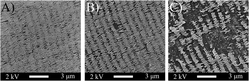
FIGURE 4. SEM images of the evolution of HSFL and LSFL depending on scan speed with a constant average laser power PL = 50 mW. (A) A slow scan speed (vscan = 0.5 mm/s) forms a continuous LSFL pattern with an almost closed MoS2 film consisting of HSFL. (B) An increase in the scan speed to vscan = 10 mm/s, and the LSFL and HSFL are still formed. The increase in the scan speed starts to separate the HSFL region from each other through ablation of material along the LSFL. (C) Even higher scanning speeds (vscan = 125 mm/s) leads to more ablation of the LSFL and HSFL patterns in the MoS2 film, leading to partial MoS2 free space in the film.
4 Conclusion
This work shows the formation of LSFL and HSFL in ALD-deposited MoS2. We determine the parameters for the laser power and the scan speed of the galvo scanner for the LIPSS formation and observe different modes of LIPSS formation. Depending on the laser power, it is possible to choose between the formation of only HSFL or a combination of HSFL and LSFL. With the selection of the scanning speed, a degree of ablation/separation of the HSFL through the LSFL can be set. Previously, simultaneous formation of HSFL and LSFL in 2D materials was observed in laser-reduced graphene oxide (Kasischke et al., 2018). Further research has to be conducted to characterize the electrical and optical properties (Calvani et al., 2014; Maragkaki et al., 2020; Skoulas et al., 2021) of the LSFL and HSFL for integration in highly sensitive photo-detectors, innovative rectifier structures, complementary inverters, or thin-film transistors and the tribological properties for applications in nanostructured thin film coatings.
Data availability statement
The original contributions presented in the study are included in the article/Supplementary Material; further inquiries can be directed to the corresponding author.
Author contributions
MB, EG, and AO contributed to the conception and design of the study. MB and JJ performed the experiments. CB guided the project concerning MoS2 growth, ALD process development and SEM characterization. MB and EG performed the data analysis. MB and EG co-wrote the manuscript. All authors contributed to the article and approved the submitted version.
Funding
The authors are grateful for funding and support from the Federal Ministry of Education and Research Germany (BMBF) BMBF-ForMikro-FlexTMDSense project, grant number 16ES1096K and the ForLab PICT2DES (grant number 16ES0941). They acknowledge support by the Open Access Publication Funds of the Ruhr-Universität Bochum.
Conflict of interest
The authors declare that the research was conducted in the absence of any commercial or financial relationships that could be construed as a potential conflict of interest.
Publisher’s note
All claims expressed in this article are solely those of the authors and do not necessarily represent those of their affiliated organizations, or those of the publisher, the editors, and the reviewers. Any product that may be evaluated in this article, or claim that may be made by its manufacturer, is not guaranteed or endorsed by the publisher.
Supplementary material
The Supplementary Material for this article can be found online at: https://www.frontiersin.org/articles/10.3389/fnano.2023.1227025/full#supplementary-material
References
Acerce, M., Voiry, D., and Chhowalla, M. (2015). Metallic 1t phase MoS2 nanosheets as supercapacitor electrode materials. Nat. Nanotechnol. 10, 313–318. doi:10.1038/nnano.2015.40
Becher, M. J. M. J., Jagosz, J., Neubieser, R.-M., Wree, J.-L., Devi, A., Michel, M., et al. (2023). Ultrashort pulse laser annealing of amorphous atomic layer deposited MoS2 films Submitted, ArXiv. doi:10.48550/arXiv.2305.11008
Beltaos, A., Kovačević, A. G., Matković, A., Ralević, U., Savić-Šević, S., Jovanović, D., et al. (2014). Femtosecond laser induced periodic surface structures on multi-layer graphene. J. Appl. Phys. 116, 204306. doi:10.1063/1.4902950
Birnbaum, M. (1965). Semiconductor surface damage produced by ruby lasers. J. Appl. Phys. 36, 3688–3689. doi:10.1063/1.1703071
Bonse, J., Kirner, S. V., Griepentrog, M., Spaltmann, D., and Krüger, J. (2018). Femtosecond laser texturing of surfaces for tribological applications. Materials 11, 801. doi:10.3390/ma11050801
Bonse, J., Krüger, J., Höhm, S., and Rosenfeld, A. (2012). Femtosecond laser-induced periodic surface structures. J. Laser Appl. 24, 042006–042007. doi:10.2351/1.4712658
Butler, S. Z., Hollen, S. M., Cao, L., Cui, Y., Gupta, J. A., Gutiérrez, H. R., et al. (2013). Progress, challenges, and opportunities in two-dimensional materials beyond graphene. ACS nano 7, 2898–2926. doi:10.1021/nn400280c
Calvani, P., Bellucci, A., Girolami, M., Orlando, S., Valentini, V., Lettino, A., et al. (2014). Optical properties of femtosecond laser-treated diamond. Appl. Phys. A 117, 25–29. doi:10.1007/s00339-014-8311-9
Emmony, D. C., Howson, R. P., and Willis, L. J. (1973). Laser mirror damage in germanium at 10.6 μm. Appl. Phys. Lett. 23, 598–600. doi:10.1063/1.1654761
Geng, J., Shi, L., Liu, J., Xu, L., Yan, W., and Qiu, M. (2023). Laser-induced deep-subwavelength periodic nanostructures with large-scale uniformity. Appl. Phys. Lett. 122, 021104. doi:10.1063/5.0138290
Geng, J., Yan, W., Shi, L., and Qiu, M. (2022). Surface plasmons interference nanogratings: Wafer-scale laser direct structuring in seconds. Light Sci. Appl. 11 (189), 1–8. doi:10.1038/s41377-022-00883-9
Gurevich, E. L., Levy, Y., and Bulgakova, N. M. (2020). Three-step description of single-pulse formation of laser-induced periodic surface structures on metals. Nanomaterials 10, 1836. doi:10.3390/nano10091836
Gurevich, E. L., Levy, Y., Gurevich, S. V., and Bulgakova, N. M. (2017). Role of the temperature dynamics in formation of nanopatterns upon single femtosecond laser pulses on gold. Phys. Rev. B 95, 054305. doi:10.1103/physrevb.95.054305
Jagosz, J., Willeke, L., Becher, M., Ostendorf, A., Plate, P., and Bock, C. (2022). Large-area deposition of thin crystalline MoS2 films on 200 mm wafers using plasma-assisted atomic layer deposition. GMM-Fachbericht 105, 21–22.
Kasischke, M., Maragkaki, S., Volz, V., Ostendorf, A., and Gurevich, E. L. (2018). Simultaneous nanopatterning and reduction of graphene oxide by femtosecond laser pulses. Appl. Surf. Sci. 445, 197–203. doi:10.1016/j.apsusc.2018.03.086
Khare, K., Brinkmann, M., Law, B. M., Gurevich, E. L., Herminghaus, S., and Seemann, R. (2007). Dewetting of liquid filaments in wedge-shaped grooves. Langmuir 23, 12138–12141. doi:10.1021/la701515u
Kim, S. W., Na, J. H., Choi, W. L., Chung, H.-J., Jhang, S. H., Choi, S. H., et al. (2016). Patterning of periodic ripples in monolayer MoS2 by using laser irradiation. J. Korean Phys. Soc. 69, 1505–1508. doi:10.3938/jkps.69.1505
Mannion, P., Magee, J., Coyne, E., O’Connor, G., and Glynn, T. (2004). The effect of damage accumulation behaviour on ablation thresholds and damage morphology in ultrafast laser micro-machining of common metals in air. Appl. Surf. Sci. 233, 275–287. doi:10.1016/j.apsusc.2004.03.229
Maragkaki, S., Skaradzinski, C. A., Nett, R., and Gurevich, E. L. (2020). Influence of defects on structural colours generated by laser-induced ripples. Sci. Rep. 10, 53. doi:10.1038/s41598-019-56638-x
Mukhtar, S. H., Wani, M. F., Sehgal, R., and Sharma, M. D. (2023). Nano-mechanical and nano-tribological characterisation of self-lubricating mos2 nano-structured coating for space applications. Tribol. Int. 178, 108017. doi:10.1016/j.triboint.2022.108017
Pan, C., Jiang, L., Sun, J., Wang, Q., Wang, F., Wang, K., et al. (2020). Ultrafast optical response and ablation mechanisms of molybdenum disulfide under intense femtosecond laser irradiation. Light Sci. Appl. 9, 80–88. doi:10.1038/s41377-020-0318-8
Radisavljevic, B., Radenovic, A., Brivio, J., Giacometti, V., and Kis, A. (2011). Single-layer MoS2 transistors. Nat. Nanotechnol. 6, 147–150. doi:10.1038/nnano.2010.279
Rahman, S., and Lu, Y. (2022). Nano-engineering and nano-manufacturing in 2d materials: Marvels of nanotechnology. Nanoscale horizons 7, 849–872. doi:10.1039/d2nh00226d
Salimon, I. A., Zharkova, E. V., Averchenko, A. V., Kumar, J., Somov, P., Abbas, O. A., et al. (2023). Nano-engineering and nano-manufacturing in 2d materials: Marvels of nanotechnology. Micromachines 14, 1036. doi:10.3390/mi14051036
Sharma, A., Verheijen, M. A., Wu, L., Karwal, S., Vandalon, V., Knoops, H. C. M., et al. (2018). Low-temperature plasma-enhanced atomic layer deposition of 2-d MoS2: Large area, thickness control and tuneable morphology. Nanoscale 10, 8615–8627. doi:10.1039/C8NR02339E
Sipe, J. E., Young, J. F., Preston, J. S., and van Driel, H. M. (1983). Laser-induced periodic surface structure. i. theory. Phys. Rev. B 27, 1141–1154. doi:10.1103/physrevb.27.1141
Skoulas, E., Tasolamprou, A. C., Kenanakis, G., and Stratakis, E. (2021). Laser induced periodic surface structures as polarizing optical elements. Appl. Surf. Sci. 541, 148470. doi:10.1016/j.apsusc.2020.148470
Sládek, J., Levy, Y., Derrien, T.-Y., Bryknar, Z., and Bulgakova, N. M. (2022). Silicon surface patterning by regular stripes of laser-induced periodic surface structures. Appl. Surf. Sci. 605, 154664. doi:10.1016/j.apsusc.2022.154664
Wang, Z., and Mi, B. (2017). Environmental applications of 2d molybdenum disulfide (MoS2) nanosheets. Environ. Sci. Technol. 51, 8229–8244. doi:10.1021/acs.est.7b01466
Zhang, S., Li, R., Yao, Z., Liao, P., Li, Y., Tian, H., et al. (2020). Laser annealing towards high-performance monolayer MoS2 and WSe2 field effect transistors. Nanotechnology 31, 30LT02. doi:10.1088/1361-6528/ab8766
Keywords: laser-induced periodic surface structures, molybdenum disulfide, femtosecond laser, atomic layer deposition, 2D materials
Citation: Becher MJMJ, Jagosz J, Bock C, Ostendorf A and Gurevich EL (2023) Formation of low- and high-spatial frequency laser-induced periodic surface structures (LIPSSs) in ALD-deposited MoS2. Front. Nanotechnol. 5:1227025. doi: 10.3389/fnano.2023.1227025
Received: 22 May 2023; Accepted: 26 June 2023;
Published: 17 July 2023.
Edited by:
Ding Zhao, Westlake University, ChinaCopyright © 2023 Becher, Jagosz, Bock, Ostendorf and Gurevich. This is an open-access article distributed under the terms of the Creative Commons Attribution License (CC BY). The use, distribution or reproduction in other forums is permitted, provided the original author(s) and the copyright owner(s) are credited and that the original publication in this journal is cited, in accordance with accepted academic practice. No use, distribution or reproduction is permitted which does not comply with these terms.
*Correspondence: Malte J. M. J. Becher, bWFsdGUuYmVjaGVyQHJ1Yi5kZQ==