 Jonghoon Lee
 Gary Kedziora
 Nicholas Glavin
 Ajit K. Roy1*
- 1Materials and Manufacturing Directorate, Air Force Research Laboratory, Wright-Patterson Air Force Base, Dayton, OH, United States
- 2ARCTOS Technology Solutions, Dayton, OH, United States
Studies of molybdenum disulfide (MoS2) gas sensor prototypes report orders of magnitude higher sensitivity toward nitrogen dioxide (NO2) over ammonia (NH3). Based on the cluster formation model and density functional theory calculations of charge transfer, NO2 was found to form a tightly bound cluster of counter charges upon carrier donation. In contrast, NH3 forms only a semi-localized cluster of counter charges over a wide area of MoS2, creating a larger collision cross section of coulomb interaction between the charge carrier and the counter charges. We discuss the potential effect of counter charge cluster localization on the efficiency of molecular doping.
1 Introduction
Ever since the prospect of single gas molecule detection was first discussed with a graphene device (Schedin et al., 2007), whose high sensitivity was partially attributed to the surface nature of graphene exposing its whole volume to the gas molecule adsorbates, a gamut of 2D materials have been examined for gas sensor applications. In particular, transition metal dichalcogenides (TMDCs) have proven to be among the best materials for 2D gas sensor applications because of their tunable electronic properties and high sensitivity at room temperature (He et al., 2012; Late et al., 2014; Ko et al., 2016; Shokri and Salami, 2016; Yang et al., 2017; Pandey et al., 2020). When exposed to the target gas, a TMDC gas sensor responds to the adsorption of target gas molecules by changing its electrical conductivity. Based on the results of Hall measurements (Schedin et al., 2007), photoluminescence (PL) spectroscopy (Mouri et al., 2013; Cho et al., 2015a; Wang et al., 2019), and theoretical considerations (Leenaerts et al., 2008; Wehling et al., 2008), the molecular gas adsorption was recognized as inducing charge transfer on TMDC and modulating the charge carrier density on the 2D device. Depending on whether the electrical conductivity of the 2D sensor was increasing or decreasing, the target gas molecule would be categorized as carrier-donating or -compensating.
Experimental studies of TMDC gas sensor devices often compare the sensitivity of the device to various kinds of gas molecules, where the sensitivity is defined as the change in electrical resistance upon gas sensing, normalized to the default resistance of the device in dry air (Cho et al., 2015a; Cho et al., 2015b; Hau et al., 2021). The dry air normalization is specifically used to reduce the amount of chemical doping from redox reactions involving water vapor. The reported sensitivity involves a significant degree of reversibility correlated with the partial pressure of the target gas molecules in the gas environment. This reversibility indicates that a corresponding amount of carrier doping is induced by the physisorption of gas molecules that readily desorb upon a decrease in the partial pressure of the target gas molecules in the air.
The most frequently targeted gas molecules in TMDC gas sensor studies are nitrogen dioxide (NO2) and ammonia (NH3) as they are the representative p-type and n-type molecular dopants. It has consistently been reported in the experimental literature that the sensitivity of TMDC gas sensors toward NO2 is an order of magnitude higher than for NH3, which holds true for both n-type and p-type TMDC devices (Cho et al., 2015a, Cho et al., 2015b; Hau et al., 2021). This means that the charge carrier density in the TMDC gas sensor is much more strongly affected by the presence of NO2 than NH3 in the gas environment under the same partial pressure. From this, it may be concluded that NO2 should be a dopant with a superior efficiency compared to NH3 and other gas molecules. However, the concept of doping efficiency as used previously is rather vague because correlating the experimentally measurable sensitivity with the partial pressure of target gas molecule in the environment involves multiple processes such as molecular adsorption and charge-state transition. In the following section, we discuss the processes involved in molecular doping and introduce counter charge cluster localization, which has been seldom mentioned in the literature, despite the fact that it can potentially affect doping efficiency.
The first event that must occur in the sensing process is the adsorption of gas molecules onto the exposed TMDC surface. The adsorption energy is the thermodynamic observable estimating the surface density of target gas molecules at equilibrium. Gas molecules with lower adsorption energy would have a greater chance of affecting the electronic properties of TMDC if the number of carriers donated or compensated positively correlated with the surface density of the gas molecules. Theoretical studies of gas molecule physisorption, however, found only nonsignificant differences (less than 10 meV) in the adsorption energies of NO2 and NH3 on TMDC (Yue et al., 2013). Therefore, the adsorption energy alone cannot be the main cause of the large differences in sensitivity of a TMDC sensor toward NO2 and NH3.
In analyzing doping efficiency, we need to measure more than the surface coverage of molecular adsorbates because not all the adsorbates are activated as dopants. The dopant activation process after adsorption results in charge transfer, for which there exist multiple plausible scenarios. The so-called chemical doping occurs especially at chemically heterogeneous reactive sites of structural defects and edges of TMDC. Integer charge transfer results from redox reactions involving not only the target gas molecule and TMDC but also ambient molecules of nitrogen, oxygen, and water (Li et al., 2017; Zhao et al., 2018). Such redox reactions are strongly dependent on ambient temperature and result in charge distribution near defects and edges, producing regions of carrier depletion and double-layer potential (Gautam et al., 2021). The other viable scenario of charge transfer involves physisorption of gas molecules, which is of our interest in this report. In this case, the so-called standard model of molecular doping examines the energies of the highest occupied molecular orbital (HOMO) and the lowest unoccupied molecular orbital (LUMO) of gas molecules relative to the Fermi level or work function of the hosting TMDC (Peng and Cho, 2000; Wehling et al., 2008; Park et al., 2019). If the LUMO of the gas molecules is lower than the Fermi level of hosting TMDC, the molecular gas adsorbate accepts electrons from TMDC. If the HOMO is higher than the Fermi level, the gas molecules become donors of electrons to TMDC. In essence, this model follows the Schottky–Mott rule of interface band bending, which interprets electron transfer as a transport phenomenon allowing two distinct bodies of electron distribution in contact to reach equilibrium (Zhang and Yates, 2012). As this charge transfer process involves the Fermi level as an electron reservoir, the efficiency of gas molecular doping becomes a function of the Fermi level.
For conventional inorganic semiconductors where the conduction is predominantly band conduction via delocalized conduction band or the valence band, thermodynamic stability analyses of dopants at various charge states are routinely performed to address the efficiency of the dopant, such as whether it is a shallow or deep donor (Van de Walle and Neugebauer, 2004; Freysoldt et al., 2014; Alkauskas et al., 2016). However, the charged dopant stability analysis is not as frequently utilized for molecular doping of 2D materials, partly because our understanding of the conduction mechanism in TMDC gas sensors is still developing. It should be noted that electrons or holes transferred to the Fermi level of TMDC are not necessarily free-charge carriers if the Fermi level exists within the localized gap states. When the transferred charges are near the Fermi level but away from delocalized bands, they still conduct electricity via ‘hopping’ conduction (Shklovskii and Efros, 1984). In fact, this variable range hopping was reported as the governing conduction mechanism of TMDC thin films when the temperature was lower than room temperature (Qiu et al., 2013; Xue et al., 2019). Even near room temperature, the variable range hopping remained as the major channel of conduction in various 2D material thin films (Negishi et al., 2014; Kovtun et al., 2021). Considering the semi-crystalline quality of TMDC materials often adopted for gas sensor applications and research, it is plausible to assume that electrical conduction occurs through the multi-channel type of band conduction and hopping conduction, where the hopping conduction channel is rather predominant.
As outlined so far, the molecular doping of charge carriers and conduction in 2D material thin films are multifaceted phenomena. The outstanding experimental challenge preventing quantitative analysis lies in identifying the several physically distinguishable mechanisms simultaneously participating in charge transfer. Nevertheless, we can attest phenomenologically that the charge transfer between the gas molecular adsorbate and the hosting 2D material results in involves charge carriers conducting electricity along with the counter charges of the donated carriers localized upon the gas molecular adsorbate. As it is localized, the counter charge left on the adsorbate does not participate in the conduction. If anything, it would more likely hamper the mobility of the free carriers through coulomb scattering. Coulomb interactions between the free carrier and localized counter charges will affect the separation and recombination between them as well. However, as the subject of counter charge distribution has rarely been studied for molecular dopants, our understanding of how this would affect the efficiency of carrier doping is limited. As a side note, for polymer semiconductors, the effect of counter-ion size on delocalization of carriers was studied, although the subject was not the distribution of counter charges but the physical size of the counter-ions (Thomas et al., 2020).
The counter charge distribution upon charge carrier donation was first studied for conventional inorganic semiconductors, providing valuable insights toward overall understanding of carrier donation with unexpected findings (Schwingenschlögl et al., 2010). For carrier doping of conventional semiconductors of silicon and diamond, group III and group IV elements often substitute the host element to compensate or donate electrons. From the theoretical analysis of counter charge distribution upon carrier doping, it was found that the carrier donation was not executed solely by the dopant element but by the cluster of atoms composed of the dopant and nearby host atoms (Schwingenschlögl et al., 2010; 2011; Smith et al., 2017).
The additional physical understanding provided by the cluster formation model distinguishes two different types of charge transfer associated with dopant–host interaction. For the example of silicon doping using arsenic, as we look into the charge distribution between arsenic atoms and nearby silicon atoms, the electron distribution is shifted away from silicon toward arsenic because arsenic has stronger electronegativity than silicon. However, in terms of carrier doping properties, arsenic is an n-type dopant donating an electron to the silicon lattice, which contradicts the direction of charge transfer based on strength of electronegativity. The cluster formation model of carrier doping resolved this apparent inconsistency, when it was found that the electron carrier was donated to the silicon lattice not by the arsenic atom alone but by a cluster of atoms including arsenic and nearby silicon atoms. Therefore, we note two distinguishable and uncorrelated charge transfers: a local charge transfer within a cluster with electrons shifting toward arsenic from silicon and a charge transfer as carrier doping between the arsenic cluster and the silicon lattice, wherein an electron moves from the arsenic cluster to the silicon lattice.
In this paper, we describe the nature of the charge transfer between a gas molecular adsorbate and 2D TMDC material based on the counter charge cluster formation model and density functional theory. Our system of interest is 2D molybdenum disulfide (MoS2) as the archetypal TMDC along with ammonia (-NH3) and nitrogen dioxide (-NO2) as the representative molecular dopants of opposing doping property. As we addressed the differences between NO2 and NH3 as molecular dopants, we directed our attention not to the donated charge carrier but rather to the counter charges left localized on the molecular dopant. Unlike the donated charge carrier whose spatio-temporal property keeps varying as it transports, the counter charge distribution left on the molecular dopant would be essentially constant, as long as other charge carriers were not nearby. As discussed in the following sections, the counter charge cluster formation analysis upon carrier doping by molecular dopants allowed us to determine the drastically different activities of NO2 and NH3. NO2 molecular adsorbates, upon donation of a hole, form a tightly localized cluster of counter charges centered around a NO2 molecule. On the contrary, the counter charge cluster formed by NH3 upon electron donation is only semi-localized and exhibits a dimension that is not well defined. The implication of such a qualitative difference on the doping efficiency is conjectured and discussed.
2 Materials and methods
To investigate the charge distribution in the gas molecular adsorbate complex, we used the Vienna ab initio simulation package (VASP) for the density functional theory (DFT) calculations (Hafner, 2008). Along with the exchange-correlation kernel of Perdew–Burke–Ernzerhof revised for solids (PBEsol), the projector augmented wave (PAW) pseudo-potentials for molybdenum (Mo) and sulfur(S) were adopted (Blöchl, 1994; Csonka et al., 2009). In this context, the electronic band gap energy of MoS2 as the difference between the valence band maximum (VBM) and the conduction band minimum (CBM) in the ground state band structure was calculated to be 1.28 eV for the bilayer with a separation distance of 6.14 Å. Additional Bader charge analysis was also performed to attribute the electron distribution to each atomic and molecular entity (Tang et al., 2009). As Bader charge analysis utilizes the gradient of charge distribution, which is grid-based in VASP, a high-resolution grid between elements is necessary in charge-density calculations to reduce errors in Bader analyses. For the high-resolution grid, VASP calculations were performed with the ‘Accurate’ setting for PREC and the energy cutoff set to 420 eV, which is 1.5 times the energy cutoff used for the molybdenum pseudo-potential, to convert the charge density on gas molecules with significant figures down to two decimal places of fundamental charge.
Figure 1 shows the ground state configurations of gas molecular physisorption widely studied and reported for MoS2 gas sensing devices. The NO2 and NH3 molecules are characterized as hole donors and electron donors, respectively. Such gas molecular adsorbates affect the trion peaks of photoluminescence (Tongay et al., 2013; Cho et al., 2015a), indicating variations in the carrier density. The configurations shown in Figure 1 were used to calculate the charge distribution. For charged systems, the periodic image charge interaction should affect the charge cluster confinement. Therefore, four different values of the supercell lattice constant (L) were used to address the system size dependency of charge distribution, as with L = 4a, 8a, 12a, 16a where a = 3.20 Å is the lattice constant of the MoS2 unit cell.
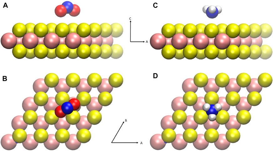
FIGURE 1. Schematic representation of gas molecules physisorbed on MoS2. The size of the MoS2 supercell is 4a × 4a, where a is the lattice constant of the MoS2 primary unit cell, 3.197Å. The atomic configuration depicted here shows the lowest energy configuration calculated (Yue et al., 2013; Zhao et al., 2014; Cho et al., 2015a). (A,B) Side and top views of nitrogen dioxide physisorption configuration. (C,D) Side and top views of ammonia physisorption configuration. Colors refer to the following: Mo (pink), S (yellow), N (blue), O (red), and H (white).
The charge distribution was calculated before and after carrier donation (Schwingenschlögl et al., 2010; 2011; Smith et al., 2017). The charge transfer before carrier donation occurred locally in the dopant complex, a region of adsorbate and nearby host elements. A weak hybridization between nearby molecular orbitals rearranges the electron distribution resulting in shifting of charges. The magnitude of such charge transfer is only fractional, however. More importantly, it does not contribute to electrical conduction because transferred charges are localized at the adsorbate complex. The charge state of the overall system remains neutral because no charge leaves the adsorbate and its surroundings. On the contrary, when charge transfer happens between the adsorbate complex and the electron reservoir of the system’s Fermi level, as in carrier donation, the adsorbate complex becomes counter charged. By analyzing the distribution of this counter charge in the adsorbate complex, we investigated the formation of the counter charge cluster.
It should be noted that our interest is in charge distribution only, not on the free energy of the charged system. Addressing free energy of the various charge states of a dopant system often assumes a single isolated dopant in an infinite host, which requires corrections of various supercell artifacts (Van de Walle and Neugebauer, 2004; Persson et al., 2005; Lany and Zunger, 2008; Freysoldt et al., 2009; 2014; Alkauskas et al., 2016). For 2D charged systems of slab and surfaces, the methodological consensus is still being sought after regarding the correction of even stronger coulomb self-interactions through a vacuum (Komsa and Pasquarello, 2013; Komsa et al., 2014; Freysoldt and Neugebauer, 2018; O’Hara et al., 2019; Rutter, 2021).
3 Results with discussion
As outlined in the Introduction section, the molecular doping via gas molecular physisorption goes through processes of adsorption and charge-state transition. Adsorption is a local event, while the transition in the charge state of the adsorbate is a process depending on the Fermi level of the host. Each process is accompanied by charge transfers with different characteristics and magnitudes, which are discussed separately in the following sections.
3.1 Adsorbate complex formation
First, we discuss the local charge transfer upon adsorption. As gas molecules approach the MoS2 substrate, weak hybridizations between molecular orbitals result in redistribution of electrons among the elements belonging to the physisorbed gas molecules and the substrate atoms near the adsorption site, satisfying the difference in electron affinity among elements involved in the specific adsorbate configuration. Quantitatively, the redistribution in electron density (Δρ) upon adsorption can be expressed as follows:
where
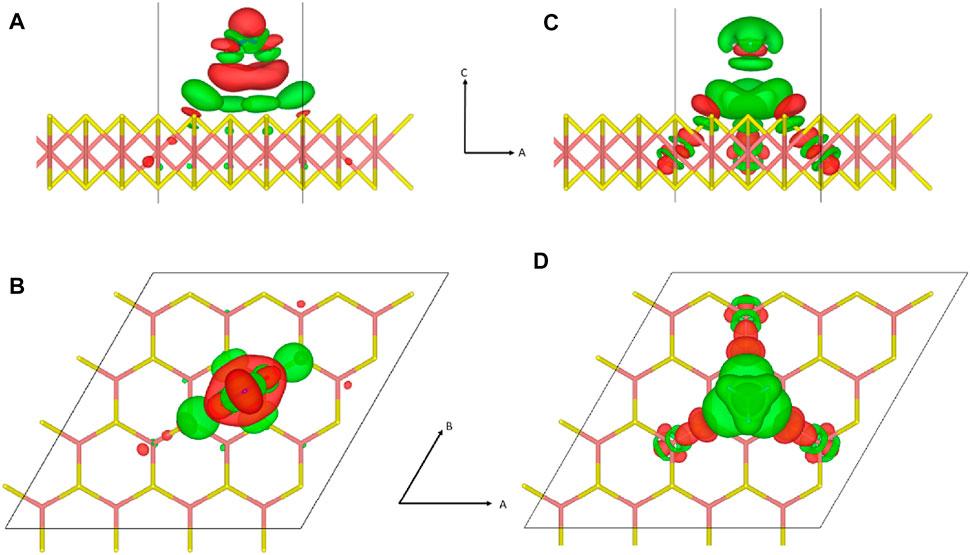
FIGURE 2. Redistribution of electrons upon physisorption of gas molecules is depicted with a density isosurface. Subfigure arrangement and atomic configurations are identical to those of Figure 1. (A,B) For NO2 adsorption, the electron density isosurface at
Applying Bader charge analysis to
More often than not, the direction of this polarization is qualitatively associated with the experimental categorization as to whether the gas molecule is an electron donor or an acceptor (Yue et al., 2013; Wang et al., 2019). However, this is only coincidental and situational because of the following reasons. First, the transferred charge is not free to be conducted because it is spatially localized near the molecular adsorbate. Second, the amount of charge transferred is fractional, representing only a few percent of the elemental charge, while the photoluminescence spectroscopy data are consistent with integer charge carrier doping with a trion peak (Cho et al., 2015a). Such minuscule amounts of fractional charge are thought to accumulate into integer charges when combined from an ensemble of dopants (Tongay et al., 2013). However, such arguments could be realized only if the transferred charge resides in the delocalized band or metal where charges are free to move and gather. Third, the direction of polarization depends on the adsorbate configuration, which contradicts the standard doping model where the doping property is independent of the adsorbate configuration (Leenaerts et al., 2008). Fourth, this hypothesis assumes that the carrier donation should happen between the gas molecule and the nearby adsorbent atoms. As observed in the counter charge cluster formation model, it is not the donor alone but a cluster of atoms including the donor and nearby host atoms that donates the carrier (Schwingenschlögl et al., 2010; 2011).
In the charge transfer depicted in Figure 2, the charge state of the whole system remains neutral because there is no change in the total number of electrons in the system. Actually, what we observe from the charge redistribution in Figure 2 is the formation of an adsorbate complex encompassing the adsorbate molecule and proximate adsorbent atoms affected by the adsorbate, which has little to do with charge carrier doping. As we refer to an analogical charge transfer, which is both fractional and local, a similar dopant complex formation can be identified in conventional silicon doping despite the difference in chemical bonding. When a group III or IV dopant atom substitutes for a silicon atom in the silicon lattice, the dopant atom forms multiple covalent bonds with nearby silicon atoms. Due to differences in the electronegativity between silicon atoms and the dopant atom, the covalent bonds of the silicon–dopant pair become polar with a fractional shifting of charges. However, this fractional rearrangement of charge distribution near the dopant atom has nothing to do with carrier doping resulting from the charge transfer between the dopant complex and the delocalized conduction or valence band of the lattice. For example, although both boron and gallium are p-type dopants in a silicon lattice, the polarity in the polar-covalent bonds in the boron–silicon pair and the gallium–silicon pair are opposite to each other because boron is more electronegative than silicon, while gallium is less electronegative than silicon (Schwingenschlögl et al., 2010). The direction of polarity in the polar-covalent bond involving a dopant atom may agree or disagree with the actual doping property of the dopant, which is only coincidental.
3.2 Counter charge cluster formation
The standard molecular doping model describes the energetically favored charge transfers between HOMO (or LUMO) of the molecular adsorbate dopant and the Fermi level of the hosting material as electron reservoir (Peng and Cho, 2000; Wehling et al., 2008; Park et al., 2019). The charge carrier, whether it is an electron or a hole donated by the molecular adsorbate to the hosting material, should participate in the electrical conduction in the host, while the counter charge of the carrier remains on the adsorbate dopant. Assuming charge transfer between the dopant and the Fermi level of the host (Schwingenschlögl et al., 2010; 2011; Smith et al., 2017), we calculated the distribution of counter charges in the supercell of MoS2 with molecular adsorbate. The counter charge distribution indicates the domain of the cluster from which the charge carrier is donated.
If the Fermi level of the system is near the delocalized conduction or valence band of MoS2, the charge transfer between the molecular adsorbate and the Fermi level will donate free carriers for band conduction in the hosting lattice. However, as hopping conduction is often reported as the major conduction mechanism in 2D TMDC thin films (Qiu et al., 2013; Xue et al., 2019; Kovtun et al., 2021), we assumed that charge transfer happened between the molecular adsorbate and other defect sites near the Fermi level. The transferred charge would conduct electricity through hopping along the percolated path of defect sites (Shklovskii and Efros, 1984). To address the counter charge distribution on the molecular adsorbate after carrier doping, we subtracted the electron density of the adsorbate system (MoS2+mole) in the neutral charge state
For the p-type dopant of the NO2 molecular adsorbate, Figure 3 shows the counter charge distribution,
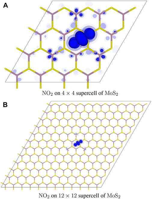
FIGURE 3. Distribution of added electrons in the NO2 adsorbate complex. Isosurfaces are rendered in different shades of blue at the three different values of:
The n-type doping of NH3 involves an electron transfer from a cluster surrounding NH3 to the Fermi level of MoS2. Figure 4 shows the distribution of counter charge,
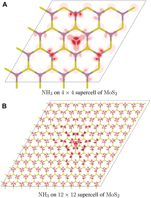
FIGURE 4. Distribution of added holes in the NH3 adsorbate complex. (A) A 4 × 4 supercell of MoS2 is used. The atomic configuration is identical to that of Figure 1D. Isosurfaces are rendered in dark, medium, and light shades of red, at three different values of
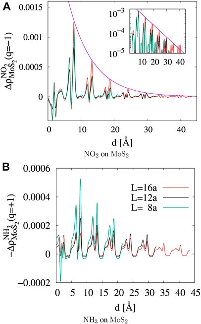
FIGURE 5. Line profile of counter charge density in MoS2 against the distance from the molecular adsorbate. The density is followed on the AB plane of MoS2 along the direction of
From Bader charge analysis, which specifies the amount of counter charge assumed by the gas molecule itself, we can estimate the Fukui index (f+/−) of gas molecular adsorbates as follows:
where Qmole(N) is the charge on a gas molecule when N is the number of electrons in the system at neutral charge state. The Fukui index estimates the electrophilicity (f+) of NO2 and the nucleophilicity (f−) of NH3 when the system is charged with additional or a reduced number of electrons (Geerlings et al., 2003). Figure 6 and Table 1 show that the electrophilicity of the NO2 molecule converges to around 0.25 with increasing system size, while the remaining 75% of electron is distributed over the MoS2 atoms in the cluster. However, the NH3 molecule shows a nucleophilicity that diminishes as the system size increases. The amount of counter charge residing on the NH3 molecule becomes negligible for an isolated NH3 adsorbate.
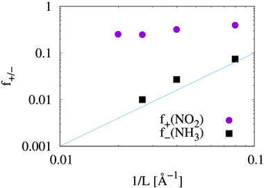
FIGURE 6. Fukui index of gas molecular adsorbates. Values from Table 1 are plotted. The solid blue line (∼ L−2) is shown for reference and not as a trend line.
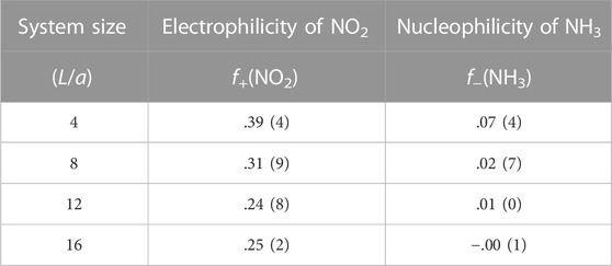
TABLE 1. Fukui index of molecular adsorbates.
Although the subject of counter charge clusters is a rare topic in the literature of molecular doping, there are multiple scenarios of possible effects of counter charge distribution and localization on charge carriers. The electrostatic interaction between the carrier and its counter charge is central to the activation and transient recombination of the carrier. The interaction between counter charges is another subject deserving of attention as its screening would affect the surface density of the activated dopants. Not only the carrier density but also the mobility of the carrier depends on counter charge distribution; the spatial dimension and strength of localization of the counter charge clusters will generate the interaction potential landscape which the carrier has to navigate through. Considering the stronger 2D coulomb interaction rendering short exciton lifespans of a few nanoseconds (Palummo et al., 2015; H-L et al., 2020), the influence of counter charge distribution on the efficiency of carrier doping deserves greater attention from the research community.
NO2 and NH3 are gas molecules with opposite doping characteristics most frequently adopted in testing gas sensor application of layered MoS2. Based on the counter charge cluster formation upon carrier donation, NO2 fits the physical picture of the standard doping model quite well, rendering a spatially well confined cluster of counter charge localized on NO2. In contrast, NH3 forms only a semi-localized cluster of counter charge centered on the molecule. It is noteworthy that these two gas molecules with vast differences in doping efficiency feature counter charge clusters of qualitatively distinguishable characteristics.
4 Conclusion
Gas sensor devices based on two-dimensional layered transition metal dichalcogenides feature desirable properties such as high sensitivity and room temperature operation. The sensing mechanism is based on the change in charge carrier density upon gas molecular adsorption. MoS2 gas sensors show an order of magnitude higher sensitivity toward NO2 over NH3 (Cho et al., 2015a; Hau et al., 2021). For the case of charge carrier doping from gas molecular physisorption, the counter charge cluster formation was investigated using density functional theory calculations of charge density. The standard doping model assumes a delocalized charge carrier with a localized counter charge at the dopant, which accords well with the p-type dopant molecule, NO2. A quarter of an elemental charge is physically distributed on the NO2 molecule, while the remaining portion of the elemental charge is distributed over the hosting MoS2 within the counter charge cluster.
The nature of the positive counter charge clusters formed by NH3 upon electron donation is very different. Although the distribution of the counter charge is centered around the NH3 adsorbate, the cluster is only semi-localized and does not have a definite size. The amount of actual counter charge possessed by NH3 molecules is actually negligible as most of the counter charge is assumed by host atoms in the cluster. Although the effect of counter charge distribution on carrier dynamics and doping has not been systematically studied, it is conjectured that the wider distribution of semi-localized counter charge may hamper the sensitivity of gas sensors by reducing the carrier mobility through an enhanced scattering cross section and also by promoting transient recombination with the delocalized carriers.
Data availability statement
The original contributions presented in the study are included in the article/Supplementary Material; further inquiries can be directed to the corresponding authors.
Author contributions
JL, NG, and AR conceived the idea of this study. JL, GK, and AR designed this study. JL developed the draft of this manuscript. All authors discussed the results and contributed to the final manuscript.
Conflict of interest
Author JL was employed by the company ARCTOS Technology Solutions.
The remaining authors declare that the research was conducted in the absence of any commercial or financial relationships that could be construed as a potential conflict of interest.
The handling editor is currently organizing a research topic with the author, AR.
Publisher’s note
All claims expressed in this article are solely those of the authors and do not necessarily represent those of their affiliated organizations, or those of the publisher, the editors, and the reviewers. Any product that may be evaluated in this article, or claim that may be made by its manufacturer, is not guaranteed or endorsed by the publisher.
References
Alkauskas, A., McCluskey, M. D., and Van de Walle, C. G. (2016). Tutorial: Defects in semiconductors—combining experiment and theory. J. Appl. Phys. 119, 181101. doi:10.1063/1.4948245
Blöchl, P. E. (1994). Projector augmented-wave method. Phys. Rev. B 50, 17953–17979. doi:10.1103/PhysRevB.50.17953
Cho, B., Hahm, M. G., Choi, M., Yoon, J., Kim, A. R., Lee, Y.-J., et al. (2015a). Charge-transfer-based gas sensing using atomic-layer MoS2. Sci. Rep. 5, 8052. doi:10.1038/srep08052
Cho, B., Kim, A. R., Park, Y., Yoon, J., Lee, Y.-J., Lee, S., et al. (2015b). Bifunctional sensing characteristics of chemical vapor deposition synthesized atomic-layered mos2. ACS Appl. Mater. Interfaces 7, 2952–2959. doi:10.1021/am508535x
Csonka, G. I., Perdew, J. P., Ruzsinszky, A., Philipsen, P. H. T., Lebègue, S., Paier, J., et al. (2009). Assessing the performance of recent density functionals for bulk solids. Phys. Rev. B 79, 155107. doi:10.1103/PhysRevB.79.155107
Freysoldt, C., Grabowski, B., Hickel, T., Neugebauer, J., Kresse, G., Janotti, A., et al. (2014). First-principles calculations for point defects in solids. Rev. Mod. Phys. 86, 253–305. doi:10.1103/RevModPhys.86.253
Freysoldt, C., and Neugebauer, J. (2018). First-principles calculations for charged defects at surfaces, interfaces, and two-dimensional materials in the presence of electric fields. Phys. Rev. B 97, 205425. doi:10.1103/PhysRevB.97.205425
Freysoldt, C., Neugebauer, J., and Van de Walle, C. G. (2009). Fully ab initio finite-size corrections for charged-defect supercell calculations. Phys. Rev. Lett. 102, 016402. doi:10.1103/PhysRevLett.102.016402
Gautam, Y. K., Sharma, K., Tyagi, S., Ambedkar, A. K., Chaudhary, M., and Pal Singh, B. (2021). Nanostructured metal oxide semiconductor-based sensors for greenhouse gas detection: Progress and challenges. R. Soc. Open Sci. 8, 201324. doi:10.1098/rsos.201324
Geerlings, P., De Proft, F., and Langenaeker, W. (2003). Conceptual density functional theory. Chem. Rev. 103, 1793–1874. doi:10.1021/cr990029p
H-L, P., Mondal, P., Bid, A., and Basu, J. K. (2020). Electrical and chemical tuning of exciton lifetime in monolayer mos2 for field-effect transistors. ACS Appl. Nano Mater. 3, 641–647. doi:10.1021/acsanm.9b02170
Hafner, J. (2008). Ab-initio simulations of materials using VASP: Density-functional theory and beyond. J. Comput. Chem. 29, 2044–2078. doi:10.1002/jcc.21057
Hau, H. H., Duong, T. T. H., Man, N. K., Thi Viet Nga, T., Thi Xuan, C., Thi Thanh Le, D., et al. (2021). Enhanced no2 gas-sensing performance at room temperature using exfoliated mos2 nanosheets. Sensors Actuators A Phys. 332, 113137. doi:10.1016/j.sna.2021.113137
He, Q., Zeng, Z., Yin, Z., Li, H., Wu, S., Huang, X., et al. (2012). Fabrication of flexible MoS2 thin-film transistor arrays for practical gas-sensing applications. Small 8, 2994–2999. doi:10.1002/smll.201201224
Ko, K. Y., Song, J.-G., Kim, Y., Choi, T., Shin, S., Lee, C. W., et al. (2016). Improvement of gas-sensing performance of large-area tungsten disulfide nanosheets by surface functionalization. ACS Nano 10, 9287–9296. doi:10.1021/acsnano.6b03631
Komsa, H.-P., Berseneva, N., Krasheninnikov, A. V., and Nieminen, R. M. (2014). Charged point defects in the flatland: Accurate formation energy calculations in two-dimensional materials. Phys. Rev. X 4, 031044. doi:10.1103/PhysRevX.4.031044
Komsa, H.-P., and Pasquarello, A. (2013). Finite-size supercell correction for charged defects at surfaces and interfaces. Phys. Rev. Lett. 110, 095505. doi:10.1103/PhysRevLett.110.095505
Kovtun, A., Candini, A., Vianelli, A., Boschi, A., Dell’Elce, S., Gobbi, M., et al. (2021). Multiscale charge transport in van der waals thin films: Reduced graphene oxide as a case study. ACS Nano 15, 2654–2667. doi:10.1021/acsnano.0c07771
Lany, S., and Zunger, A. (2008). Assessment of correction methods for the band-gap problem and for finite-size effects in supercell defect calculations: Case studies for ZnO and GaAs. Phys. Rev. B 78, 235104. doi:10.1103/PhysRevB.78.235104
Late, D. J., Doneux, T., and Bougouma, M. (2014). Single-layer MoSe2 based NH3 gas sensor. Appl. Phys. Lett. 105, 233103. doi:10.1063/1.4903358
Leenaerts, O., Partoens, B., and Peeters, F. M. (2008). Adsorption ofH2O, NH3, CO, NO2, and no on graphene: A first-principles study. Phys. Rev. B 77, 125416. doi:10.1103/PhysRevB.77.125416
Li, X., Li, X., Li, Z., Wang, J., and Zhang, J. (2017). WS2 nanoflakes based selective ammonia sensors at room temperature. Sensors Actuators B Chem. 240, 273–277. doi:10.1016/j.snb.2016.08.163
Mouri, S., Miyauchi, Y., and Matsuda, K. (2013). Tunable photoluminescence of monolayer MoS2 via chemical doping. Nano Lett. 13, 5944–5948. doi:10.1021/nl403036h
Negishi, R., Akabori, M., Ito, T., Watanabe, Y., and Kobayashi, Y. (2016). Band-like transport in highly crystalline graphene films from defective graphene oxides. Sci. Rep. 6, 28936. doi:10.1038/srep28936
O’Hara, A., Tuttle, B. R., Zhang, X.-G., and Pantelides, S. T. (2019). Formation energies of charged defects in two-dimensional materials – resolution of long-standing difficulties. doi:10.48550/ARXIV.1911.11192
Palummo, M., Bernardi, M., and Grossman, J. C. (2015). Exciton radiative lifetimes in two-dimensional transition metal dichalcogenides. Nano Lett. 15, 2794–2800. doi:10.1021/nl503799t
Pandey, S. K., Das, R., and Mahadevan, P. (2020). Layer-dependent electronic structure changes in transition metal dichalcogenides: The microscopic origin. ACS Omega 5, 15169–15176. doi:10.1021/acsomega.0c01138
Park, S., Schultz, T., Xu, X., Wegner, B., Aljarb, A., Han, A., et al. (2019). Demonstration of the key substrate-dependent charge transfer mechanisms between monolayer mos2 and molecular dopants. Commun. Phys. 2, 109. doi:10.1038/s42005-019-0212-y
Peng, S., and Cho, K. (2000). Chemical control of nanotube electronics. Nanotechnology 11, 57–60. doi:10.1088/0957-4484/11/2/303
Persson, C., Zhao, Y.-J., Lany, S., and Zunger, A. (2005). n-type doping of CuInse2 and CuGase2. Phys. Rev. B 72, 035211. doi:10.1103/PhysRevB.72.035211
Qiu, H., Xu, T., Wang, Z., Ren, W., Nan, H., Ni, Z., et al. (2013). Hopping transport through defect-induced localized states in molybdenum disulphide. Nat. Commun. 4, 2642. doi:10.1038/ncomms3642
Rutter, M. J. (2021). Charged surfaces and slabs in periodic boundary conditions. Electron. Struct. 3, 015002. doi:10.1088/2516-1075/abeda2
Schedin, F., Geim, A. K., Morozov, S. V., Hill, E. W., Blake, P., Katsnelson, M. I., et al. (2007). Detection of individual gas molecules adsorbed on graphene. Nat. Mater 6, 652–655. doi:10.1038/nmat1967
Schwingenschlögl, U., Chroneos, A., Schuster, C., and Grimes, R. W. (2011). Doping and cluster formation in diamond. J. Appl. Phys. 110, 056107. doi:10.1063/1.3633223
Schwingenschlögl, U., Chroneos, A., Schuster, C., and Grimes, R. W. (2010). Extrinsic doping in silicon revisited. Appl. Phys. Lett. 96, 242107. doi:10.1063/1.3455313
Shklovskii, B. I., and Efros, A. L. (1984). Electronic properties of doped semiconductors. Springer Berlin, Heidelberg.
Shokri, A., and Salami, N. (2016). Gas sensor based on MoS2 monolayer. Sensors Actuators B Chem. 236, 378–385. doi:10.1016/j.snb.2016.06.033
Smith, J. S., Budi, A., Per, M. C., Vogt, N., Drumm, D. W., Hollenberg, L. C. L., et al. (2017). Ab initio calculation of energy levels for phosphorus donors in silicon. Sci. Rep. 7, 6010. doi:10.1038/s41598-017-06296-8
Tang, W., Sanville, E., and Henkelman, G. (2009). A grid-based bader analysis algorithm without lattice bias. J. Phys. Condens. Matter 21, 084204. doi:10.1088/0953-8984/21/8/084204
Thomas, E. M., Peterson, K. A., Balzer, A. H., Rawlings, D., Stingelin, N., Segalman, R. A., et al. (2020). Effects of counter-ion size on delocalization of carriers and stability of doped semiconducting polymers. Adv. Electron. Mater. 6, 2000595. doi:10.1002/aelm.202000595
Tongay, S., Zhou, J., Ataca, C., Liu, J., Kang, J. S., Matthews, T. S., et al. (2013). Broad-range modulation of light emission in two-dimensional semiconductors by molecular physisorption gating. Nano Lett. 13, 2831–2836. doi:10.1021/nl4011172
Van de Walle, C. G., and Neugebauer, J. (2004). First-principles calculations for defects and impurities: Applications to III-nitrides. J. Appl. Phys. 95, 3851–3879. doi:10.1063/1.1682673
Wang, Y., Slassi, A., Stoeckel, M.-A., Bertolazzi, S., Cornil, J., Beljonne, D., et al. (2019). Doping of monolayer transition-metal dichalcogenides via physisorption of aromatic solvent molecules. J. Phys. Chem. Lett. 10, 540–547. doi:10.1021/acs.jpclett.8b03697
Wehling, T. O., Novoselov, K. S., Morozov, S. V., Vdovin, E. E., Katsnelson, M. I., Geim, A. K., et al. (2008). Molecular doping of graphene. Nano Lett. 8, 173–177. doi:10.1021/nl072364w
Xue, J., Huang, S., Wang, J. Y., and Xu, H. Q. (2019). Mott variable-range hopping transport in a mos2 nanoflake. RSC Adv. 9, 17885–17890. doi:10.1039/c9ra03150b
Yang, S., Jiang, C., and Wei, S.-h. (2017). Gas sensing in 2D materials. Appl. Phys. Rev. 4, 021304. doi:10.1063/1.4983310
Yue, Q., Shao, Z., Chang, S., and Li, J. (2013). Adsorption of gas molecules on monolayer MoS2 and effect of applied electric field. Nanoscale Res. Lett. 8, 425. doi:10.1186/1556-276X-8-425
Zhang, Z., and Yates, J. T. (2012). Band bending in semiconductors: Chemical and physical consequences at surfaces and interfaces. Chem. Rev. 112, 5520–5551. doi:10.1021/cr3000626
Zhao, S., Li, Z., Wang, G., Liao, J., Lv, S., and Zhu, Z. (2018). Highly enhanced response of MoS2/porous silicon nanowire heterojunctions to NO2 at room temperature. RSC Adv. 8, 11070–11077. doi:10.1039/C7RA13484C
Keywords: gas sensor, molybdenum disulfide, molecular doping, density functional theory, charge transfer, counter charge cluster
Citation: Lee J, Kedziora G, Glavin N and Roy AK (2023) Counter charge cluster formation in molecular doping of molybdenum disulfide. Front. Carbon 1:1089955. doi: 10.3389/frcrb.2022.1089955
Received: 04 November 2022; Accepted: 02 December 2022;
Published: 09 January 2023.
Edited by:
Ahmed Makradi, Luxembourg Institute of Science and Technology (LIST), LuxembourgReviewed by:
Julian David Correa, Universidad de Medellín, ColombiaJihyun Kim, Seoul National University, South Korea
Copyright © 2023 Lee, Kedziora, Glavin and Roy. This is an open-access article distributed under the terms of the Creative Commons Attribution License (CC BY). The use, distribution or reproduction in other forums is permitted, provided the original author(s) and the copyright owner(s) are credited and that the original publication in this journal is cited, in accordance with accepted academic practice. No use, distribution or reproduction is permitted which does not comply with these terms.
*Correspondence: Jonghoon Lee, am9uZ2hvb24ubGVlLjEuY3RyQGFmcmwuYWYubWls; Ajit K. Roy, QWppdC5Sb3lAYWZybC5hZi5taWw=