 Hezekiah Austin1*
 Chris Major1,2Colter Barney1Justin Williams1
 Zachary Becker1Mackenzie Smith1
 Brock LaMeres1,2
- 1Radiation Tolerant Computing Laboratory, Electrical and Computer Engineering Department, Montana State University, Bozeman, MT, United States
- 2Research and Development Department, Resilient Computing, Bozeman, MT, United States
Single-event upsets (SEUs) from radiation strikes in configuration memory are potentially catastrophic due to their widespread effects. For field-programmable gate arrays (FPGAs), faults in configuration memory propagate into the implemented logic design at the hardware interconnection level, leading to unpredictable results. Two payloads consisting of a pair of quad modular redundant (QMR) FPGA-based processor were deployed to the International Space Station (ISS) for 13 months. During operation, these payloads experienced a number of faults from radiation, including one payload that experienced a rare multi-core fault. Investigation suggested that the multi-core fault was the result of a single-event effect (SEE), either directly in a voter on the logic design or as an SEE in the FPGA configuration memory changing the implemented logic. An injection procedure for the FPGA’s configuration memory was developed to simulate radiation strikes and test fault detection. The injection procedure was paired with the QMR processor. This provided a full configuration memory testing environment, where the implemented logic design was capable of detecting faults propagating from the FPGA’s configuration memory. Injection throughout the configuration memory was used to create a map of particularly vulnerable locations in configuration memory and the implemented logic design. Testing with injected faults produced similar results to the multi-core fault observed in orbit on the payload. The testing procedure provides a comprehensive testing strategy, which pairs systematic injection in configuration memory with a logic design capable of detecting the induced errors to localize the propagating fault in the design.
1 Introduction
Aerospace computers operating in a harsh radiation environment generally require extensive protection and recovery methods to survive radiation strikes. The increasing number of satellites and the expense of standard protection methods, such as radiation hardening, have led to the development of low-cost alternatives. These alternatives trade protection for lower cost, power, and mass requirements. Aerospace computers are increasingly using commercial off-the-shelf (COTS) parts, particularly computer systems for low-power
2 Background, materials, and methods
2.1 Background
2.1.1 Radiation effects
Inside harsh radiation environments, computer systems are bombarded with both low-energy and high-energy electrons, protons, and heavy ions, resulting in material damage and faulted logic values (Barth et al., 2003; Johnston, 1998). Radiation-induced faults in aerospace computers fall into two general categories: total ionizing dose (TID) and single-event effects (SEEs). A TID is caused by lower-energy particles depositing charge inside the semiconductor’s installation layers (Hughes and Benedetto, 2003). An SEE occurs when a high-energy particle or heavy ion strikes the device, causes a logic-level transition, and the transition is captured. TIDs are generally a gradual failure due to the cumulative effects of lower-energy particle strikes, and SEEs are generally a temporary failure due to the immediate effects of high-energy particle strikes (Claeys and Simoen, 2002). The effects of TIDs and SEEs in a complementary metal-oxide-semiconductor (CMOS) device are shown in Figure 1.
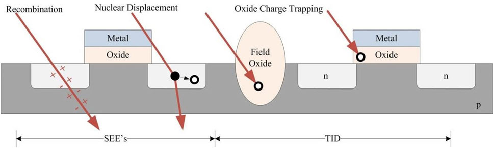
Figure 1. Effects of TIDs and SEEs in CMOS cross section (LaMeres, 2012).
Modern semiconductors have an increased resistance to TID and are inherently more vulnerable to SEEs. The current design size of semiconductor transistors (<65 nm) makes TID statistically unlikely due to reduced feature sizes (Liu et al., 2017; Zhang et al., 2017; Zhang et al., 2016). These smaller features decrease the likelihood of low-energy particles being trapped in the insulating regions of the devices (Barnaby, 2006). The vulnerability to SEEs is increased as the smaller feature sizes make particle strikes more likely to be captured, especially in combinational logic circuits (Benedetto et al., 2006). The implemented logic designs on FPGAs are primarily combinational logic circuits, making FPGAs vulnerable to SEEs during space operations. Single-event upsets, where a radiation strike flips a bit in memory, are particularly vulnerable as FPGA-implemented logic designs depend on configuration memory (Jing et al., 2012).
2.1.2 FPGA configuration memory
FPGAs have emerged as a technology capable of supporting fault recovery procedures and delivering high performance in inexpensive COTS packages. The radiation tolerance techniques used for FPGA-based, aerospace computers include system redundancy, voters, error correction codes (ECCs), cyclic redundancy check (CRC), and memory scrubbing (Yarzada et al., 2022). Combining these techniques allows for an FPGA-based computer architecture to meet the demand for radiation-tolerant, low-power, high-performance, and relatively inexpensive computers in space. A weakness of this approach is that the FPGA’s configuration memory is a single point of failure for the whole system. Within an FPGA, the configuration memory actively controls the implementation of the logic design in real time. Changes in the configuration memory immediately cascade into the logic design and induce errors. These errors fall into three categories: detectable and repairable, detectable and unrepairable, and undetectable. Detectable errors cause changes in the outputs of the logic design. Depending on the recovery techniques integrated into the system, it will either detect the errors and repair them during operation or require a full reconfiguration to clear out the issue. Detectable errors are generally caused by faults in the area of configuration memory used by the logic design. Rare cases outside the used area occur when elements outside the logic design are connected to the design by a fault. Undetectable errors are outside the used configuration memory area and result in isolated modifications on the FPGA fabric that do not connect with the implemented design. As FPGAs have millions of locations in configuration memory, the majority of faults are of this type. Furthermore, the implemented design’s response to all possible faults in the configuration memory vs. faults in the logic design is generally not tested due to time and cost constraints.
For space operations, this lack of information on the computer’s response to faults in the configuration memory makes it difficult to verify the causes of a fault during space operations. Systematic testing of this configuration memory represents an important method of verification between ground and space results. Radiation chamber testing is generally too expensive for FPGA design verification and does not ensure that every location in the configuration memory will be faulted by a radiation strike. Furthermore, FPGA designs are created using hardware description languages (HDLs) and are easily modifiable. Modern synthesis tools automatically convert the HDL into logic circuitry and map it into the resources of the FPGA. The designer has little control over how the logic is ultimately assigned, which poses a challenge for developing a consistent verification strategy. Slight changes in the HDL can cause an FPGA design to be implemented with a completely different placement on the board. The lack of a consistent verification strategy causes a major bottleneck in development due to the time and resources required for repeated, expensive testing. Therefore, FPGA-based aerospace computer development needs a fault injection system capable of injecting faults into every bit of an FPGA’s configuration memory and monitoring the resulting failures.
2.1.3 Research focus
In this paper, we propose and detail a fault injection system to stress-test an FPGA-based computer’s configuration memory scrubber and to monitor the resulting faults in the computer architecture. This procedure is specifically designed for the Xilinx Artrix 7 FPGA and the RadPC RISC-V computer architecture, and focuses on single-event upsets in the FPGA configuration memory that affect the implemented logic design. The proposed strategy has two major prerequisites: the FPGA configuration memory needs to be accessible for the fault injection, recovery, and reporting; and the logic design must support locating and reporting errors propagating from configuration memory into the logic design.
The injections were performed on the RadPC, an FPGA-based computer developed for aerospace application. This computer architecture utilizes COTS components on a small-form-factor PCB. RadPC implements a quad modular redundant (QMR) system using four softcores: CRCs and ECCs for memory checking, a data memory scrubber, and a configuration memory scrubber. Two payloads were deployed to the International Space Station (ISS) as part of overall testing for this RadPC FPGA-based computer. Additionally, an identical payload was tested on the ground under laboratory conditions. The purpose of this testing is to confirm the scrubber’s detection/recovery capabilities for the FPGA’s distributed configuration memory and provide a comparison point for the results from RadPC payloads deployed to space. This testing serves to identify critical injection locations that cause detectable and unrepairable faults in RadPC’s implemented logic. These critical injection locations allow for precise stress testing of specific components in the logic circuit design. The injection testing in the laboratory was analyzed and compared to the data from the two ISS payloads to identify potential faults in configuration memory due to radiation strikes.
This approach relies heavily on the Xilinx Soft Error Mitigation (SEM) Controller to inject faults into the FPGA’s configuration memory. The primary advantage of this system is the development of a foundation for integrating configuration memory monitoring and testing into the RadPC computer architecture. This will allow future development to integrate configuration memory reporting into a recovery method for the overall system.
2.2 Materials: payload design
The radiation-tolerant single-board computer was used in both the configuration memory experiment and the ISS mission payloads. The experiment and mission occurred in parallel. Experiment results were used to categorize mission data. Additionally, the experiment setup was used to extensively test the FPGA configuration memory and develop a new systematic testing strategy for future missions.
2.2.1 ISS payload mission
The ISS mission consisted of two payloads designed to test the RadPC computer architecture under space radiation conditions. These payloads were developed in partnership with Stottler Henke Associates, Inc (Stottler-Henke). For the experiment, Stottler-Henke developed the algorithm, and Montana State University (MSU) developed and provided the RadPC computer architecture for implementation. NanoRacks also provided the liaison with NASA for the payload launch, deployment to the ISS, and return to Earth. Payloads 1 and 2 were deployed to the ISS and remained aboard for 5 months and 13 months, respectively. The installation of payload 2 by US Astronaut Kayla Barron on 22 February 2023 is shown in Figure 2.
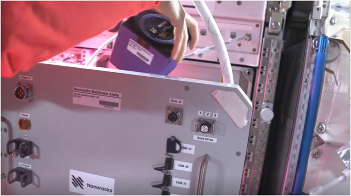
Figure 2. Payload 2 installation on ISS (LaMeres, 2023).
The objectives of the ISS project were four-fold. The first objective was testing the latest iteration of the RadPC computer architecture in a natural space radiation environment. This objective was accomplished with the deployment of the first and second payloads on the ISS. Analysis of the data and the results are included in the following sections.
The second objective was coding and executing an algorithm on the RadPC computer that utilized both inputs and outputs. Partnering with an external company for the algorithm development allowed the RadPC computer to be tested for ease of use. This objective was accomplished by a partnership with Stottler-Henke for the development of an algorithm and testing the ease of programming of the RadPC computer. Stottler-Henke developed the algorithm run on the RadPC Rev. 4 PCB, as shown in Figure 3a, for both payloads, and the MSU team used the level of support required for algorithm development and Stottler-Henke’s feedback to evaluate RadPC’s ease of programming.
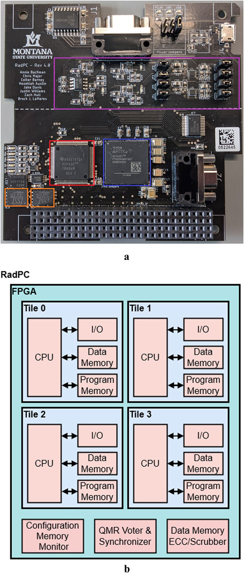
Figure 3. RadPC hardware and computer architecture: (a) RadPC Rev. 4 PCB and (b) RadPC: computer architecture.
The third objective of the ISS project was to develop a reusable design to interface with NanoRacks’ ISS internal payload system. This objective was accomplished with the design of a PCB, which provides power regulation and communication with the NanoRacks’ internal payload system on the ISS. The PCB for this interface will allow future projects to focus more on experiment development instead of interface development.
2.2.1.1 1U case shielding and ISS radiation environment
The PCB stack was encased in a 1U NanoLab’s aluminum case, with anodized sides and 3D printed endcaps. This provided the mechanical support for the PCB stacks, and the bottom endcap included power and data plugins for the payload. The aluminum case increased the amount of shielding on the payload. However, SEEs are caused by high-energy particles which are capable of passing through the space station, aluminum case, and the integrated circuit. The radiations which primarily cause SEEs—gamma rays, X-rays, and neutron rays—are all capable of penetrating aluminum. As aluminum is the main material used for the ISS’ hull, the NanoRacks’ internal payload case, and the 1U NanoLab payload case, the shielding can only reduce the radiation by a small amount.
The radiation environments for the ISS was modeled using the Cosmic Ray Effects on Micro-Electronics code (CREME96), the dimensions of the Artix-7 XC7A35T chip, and the Vivado software suite’s essential bit count for RadPC as shown in Table 1. (Major et al., 2021). Payload operation on the ISS occurred during a quiet solar cycle. Although deployment of the experiment to the ISS during this quiet solar cycle is not ideal, essential bit flips would still average 8.7 per device per day.
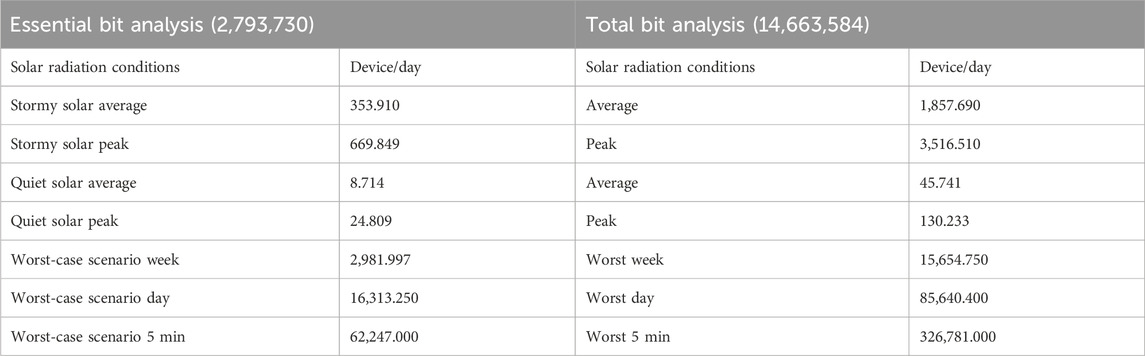
Table 1. CREME96 modeling of ISS-orbit radiation environments 30% microprocessor derating (Major et al., 2021).
Not all essential bit flips will trigger a softcore tile fault. However, RadPC is estimated to have approximately three to four softcore tile faults per device per day during payload operation.
2.2.1.2 Design of RadPC
The RadPC computer architecture was developed by Montana State University for aerospace applications. It consists of an FPGA with a QMR computer architecture that implements a juggling architecture, memory scrubbers to recover from SEEs, and a microcontroller to control data transmission, resets, FPGA reconfiguration, etc. The firmware implemented on the FPGA for the ISS payloads represented the latest iteration of the RadPC computer architecture as of September 2021. The development objective of RadPC is to provide radiation tolerance using off-the-shelf components via redundancy, scrubbing, and a recovery system. RadPC’s computer architecture utilizes redundant, synchronized cores, with an output voter, a data memory scrubber, and a configuration memory monitor. This computer architecture uses a QMR computer system implemented on an FPGA. The inherent resistance to TID in modern FPGAs from the circuit design size allows RadPC to focus mainly on detection and recovery from SEEs. The architecture of RadPC combines the strategies of a juggling architecture with an expansion of TMR and the implementation of memory scrubbing on an FPGA (Major et al., 2021). With TMR, the individual system is triplicated and the output is voted on with the majority of vote passing through as the overall system output. However, the TMR approach is not sufficient to effectively mitigate the effects of radiation on an FPGA’s implemented logic circuit or configuration memory (Sterpone and Violante, 2005). RadPC counters the vulnerability of TMR and expands on it by adding a fourth tile for QMR. Figure 4 shows the block diagram of RadPC at the board level.
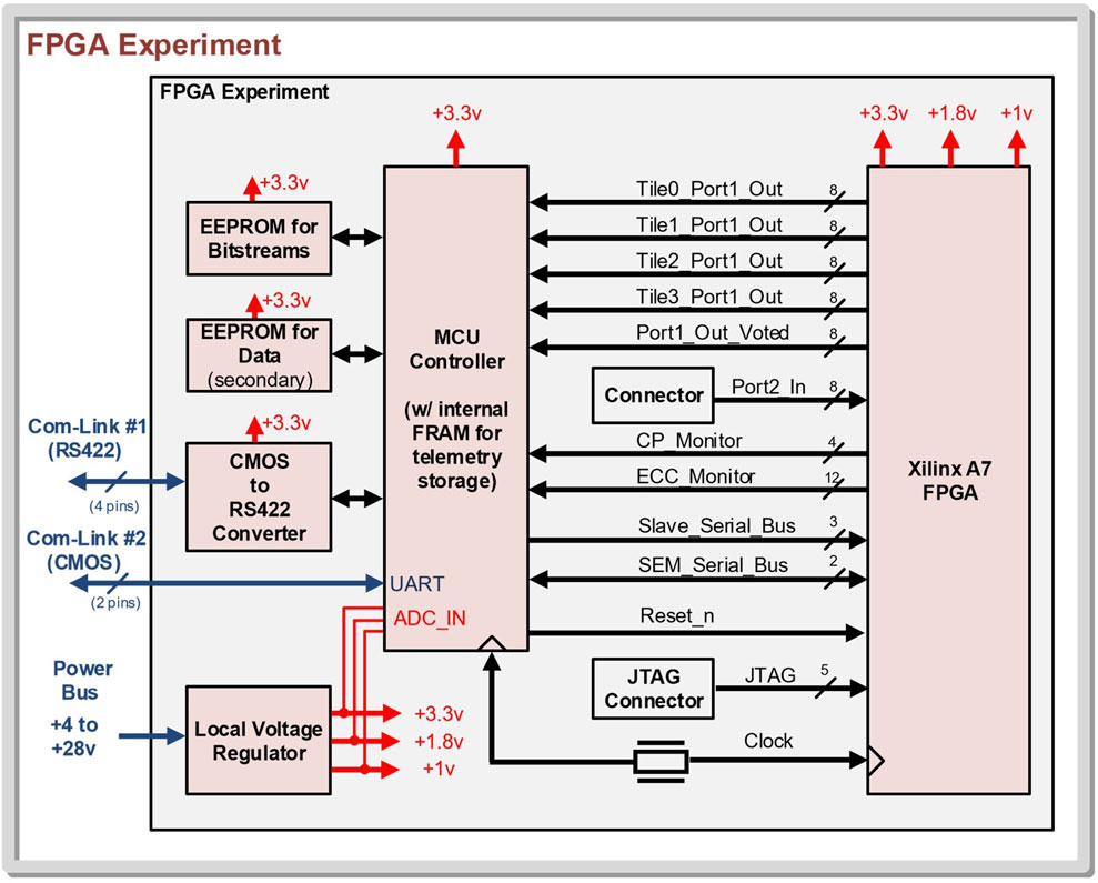
Figure 4. RadPC: individual tile (LaMeres, 2012).
The four tiles are implemented on a Xilinx FPGA. Each tile is a MicroBlaze Softcore, which is a black box processor developed by Xilinx for their FPGAs. The inclusion of the fourth tile increases the likelihood of recovery in the event of multiple SEEs in two separate tiles occurring simultaneously or successively during voting. An MSP430 microcontroller functions as the micro-controller unit (MCU) of the board. The MCU controls the serial flash memory chips containing the bitstreams and the telemetry data packet storage.
A voter is used to implement the QMR system to ensure the computer is operating with a minimal of a TMR system even during recovery. Upon reaching a software checkpoint, the voter pauses the tiles, compares the tile outputs, and votes for the majority. If a tile disagrees with the majority, recovery procedures are started. The juggling architecture uses the undamaged tiles to reset the faulted tile (Garvie and Thompson, 2004). Depending on the number of tiles being faulted, the voter triggers partial reconfiguration (PR) and memory scrubbing, or full reconfiguration (FR). Table 2 shows the recovery procedures for all possible voted tile outputs.
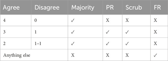
Table 2. Recovery procedures for voted outputs.
The following paragraph outlines RadPC’s response for each case in the above table. Figure 3b provides a visual block diagram of tiles and components triggering and undergoing recovery procedures.
In the first case given in the table, all tile outputs agree, and the voter achieves a majority. There is no fault to recover from, and the voter allows the tiles to resume operation. In the second case, three tile outputs agree, and the voter achieves a majority with the fourth tile undergoing recovery procedures. This consists of the SEM controller for the configuration memory being paused, the faulted tile being partially reconfigured, and the data memory scrubber checking the data memory of all four tiles. For PR, the voter sends a request to the MCU to rebuild the faulted tile. The MCU pulls the tile’s partial bitstream from the serial flash memory chip and loads it into the configuration memory. Once in the configuration memory, the current logic architecture of the FPGA is wiped, including the tile’s data memory, and the new architecture described by the partial bitstream is implemented. The data memory scrubber sits outside the tile alongside the voter. Each individual tile has its own data memory implemented inside the FPGA’s memory blocks. To bring the faulted tile back into synchronization with the other tiles, the data memory scrubber compares the data memory from each tile, votes for a majority, and overwrites incorrect entries with entries from the memory of a correct tile. The data memory scrubber walks through all memory addresses until the data memories of all tiles match. Once the memory recovery is completed, the voter allows the tiles to resume operation. For the third case, two tile outputs agree, and the voter achieves a majority with those tiles. The other two tiles disagree with both each other and the majority. These tiles undergo the same recovery procedures outlined in the second case for the faulted tile. In all other cases, the voter is not able to determine which tiles are faulted and triggers an FR of the FPGA. This follows the same procedure as PR with a request being sent to the MCU for an FR. The primary difference is that a PR uses the data memory scrubber to bring a faulted tile up to speed, ensuring that no data are lost during recovery. An FR forces any program running on RadPC-Lunar on the FPGA to completely restart.
A key point is that RadPC has two memory scrubbers: one that is part of the tile recovery procedures and another for the FPGA’s configuration memory. The data memory scrubber is an integrated part of the voter and is only operational during recovery procedures after a PR. The second memory scrubber is the SEM controller, which is completely separate from the voter and scrubs only the configuration memory on the FPGA. The SEM controller is continuously operational, except during the PR and FR recovery procedures. During PR and FR, the SEM controller is paused for the duration to avoid write/read conflicts between the SEM controller and MCU. The MCU will write either a full or a partial bitstream of the serial flash memory chip to the configuration memory. The configuration memory of the FPGA is used to hold the full bitstream for RadPC and partial bitstreams for individual tiles. During normal operations, the SEM controller scans the configuration memory, repairs faulted bits, and injects a fault into the configuration memory.
2.2.1.3 PCB stack
The hardware for the ISS project was a PCB stack consisting of three boards: Interface Board, Lunar Board, and Stottler Board, as shown in Figure 5b. Within this PCB stack, each board focused on one or more of the three major objectives for the ISS project. The Lunar Board focused on the implementation and testing of the latest firmware of the RadPC computer architecture in a natural space radiation environment. This firmware consisted of the latest VHSIC Hardware Description Language (VHDL) design for RadPC as of September 2021, named RadPC-Lunar. The Stottler Board focused on the implementation of the Stottler-Henke-developed algorithm for RadPC. This software algorithm was a C program developed to run on a modified version of the RadPC-Lunar firmware, named RadPC-AI. Onboard the ISS, RadPC-AI was used to test the RadPC computer architecture’s capability to function in a radiation environment while executing a complex algorithm to be tested. Finally, the Interface Board focused on power regulation and communication with the NanoRacks’ internal payload system on the ISS. Communication was handled by a Raspberry Pi Zero mounted on the Interface Board. Power regulation was handled by a circuit using three buck-boost switching regulators to provide 2.5 V, 3.3 V, and 5.0 V to the Raspberry Pi and RadPC PCBs.
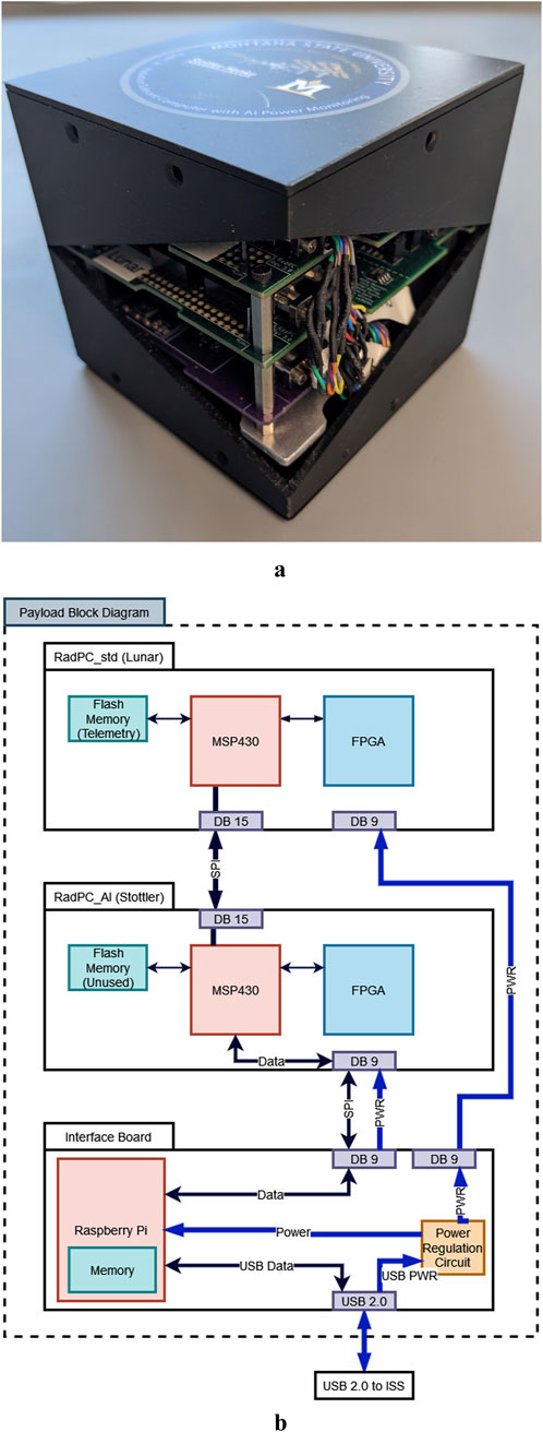
Figure 5. ISS payload model and diagram: (a) ISS engineering model and (b) ISS payload PCB stack diagram.
The innermost PCB of the stack is Lunar Board, labeled as RadPC_std (Lunar) in Figure 5b. The hardware for this board is the RadPC Rev. 4 PCB. It utilizes the RadPC-Lunar computer architecture written in VHDL for its firmware. The software for this board is a counter program written in the C programming language. RadPC-Lunar was used in the ISS project as a method of both developing VHDL for the RadPC computer architecture and providing real-world testing of both the RadPC Rev.4 PCB and RadPC-Lunar computer architecture. During operation, the Lunar Board runs the counter program and builds data packets which are transmitted to the Stottler Board for analysis. The primary purpose of the Lunar Board was to test the latest iteration of the RadPC computer architecture in a space radiation environment.
The center PCB of the stack is the Stottler Board. This board uses the same RadPC Rev. 4 PCB, a modified version of the RadPC-Lunar firmware, and a C program developed by Stottler-Henke for its software. The only difference between RadPC-Stottler and RadPC-Lunar is that the RadPC-Stottler’s board was changed to allow the telemetry data packets to be received from the Lunar Board, the enforcement of software checkpoints for synchronization, and the limitation of no serial communications. This allowed the algorithm to run on the RadPC-Lunar with the full QMR system and tile software checkpoints while receiving data from the Lunar Board. During operation on the ISS, the Stottler Board used its algorithm to evaluate the Lunar Board’s data packets and appended the result to the data packet before passing data on to the Interface Board. The PCB stack is shown in Figure 5a.
The Interface Board controls power regulation and data storage for the payload as a whole. It functions as the interface among the experiment portion of the payloads, the Lunar and Stottler boards, and the NanoRacks ISS internal payload system. Interfacing with NanoRacks was accomplished with a power regulation circuit and a Raspberry Pi Zero mounted on a PCB. The power regulation circuit provided protection against voltage or current spikes and regulated the incoming power supplied by the NanoRacks’ internal payload system to a clean 5 V for the RadPC boards and the Raspberry Pi Zero. This Raspberry Pi Zero functioned as a data storage and communication node between the experiment and NanoRacks’ systems. For the Stottler Board, the Raspberry Pi Zero functioned as a serial port using the Serial Peripheral Interface (SPI) protocol. To the ISS NanoRacks’ system, the Raspberry Pi Zero functioned as a USB flash drive, which would update itself with new data files on a daily basis.
2.2.2 Mission overview
The mission consisted of two payloads delivered to the ISS for testing in a space radiation environment. An engineering model of the completed payloads with a 3D-printed case standing in for the aluminum shell is shown in Figure 5a. This project was made possible through the collaborations and contributions of three partners: MSU, NanoRacks Inc (NanoRacks), and Stottler-Henke. The payloads were developed in a 1U CubeSat size for deployment in NanoLab on the ISS. Each payload consisted of two radiation-tolerant single-board computers: one running a counter program and the second running power analysis on the other board, and an interface board connecting with the NanoLab control computer.
2.3 Methods: configuration memory testing
On an FPGA, slight modifications in the logic design lead to large alterations in the configuration memory upon implementation. Even minor changes such as routing between components or moving components require that a completely new bitstream be generated and loaded into the configuration memory. Compared to the previous bitstream, the new bitstream would have different essential bits, which actually cause changes in the implemented logic design. The locations of critical bits, essential bits that cause detectable faults in the implemented RadPC-Lunar computer architecture, are also altered with a new bitstream. Overall, RadPC requires a more robust fault injection system for simulating SEEs in the FPGA’s configuration memory. Using the SEM controller, RadPC requires a systematic way of testing the configuration memory for critical locations that lead to tile output errors in an FPGA’s implemented logic design. Furthermore, this testing method should be repeatable for future iterations of RadPC. The development of this testing method is the memory project.
2.3.1 Experiment design
The RadPC Rev.4 PCB (RadPC PCB) was used as the basis for this experiment. Configuration memory testing was conducted using AMD Xilinx’s SEM controller on an Artrix-7 FPGA, with the RadPC-Lunar computer architecture implemented. The block diagram of the testing setup is shown in Figure 6.
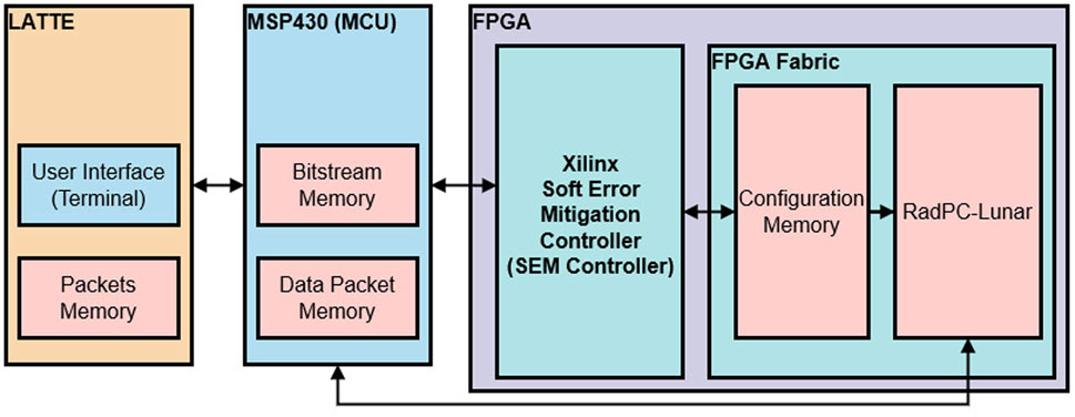
Figure 6. Block diagram of the experiment setup.
Simulation of radiation-induced faults was conducted via the SEM controller used by Xilinx FPGAs. This system injects faults by executing a NOT operation on a single bit in configuration memory. Changes in the configuration memory propagate to the implemented computer architecture on the FPGA. This makes the configuration memory particularly vulnerable to SEEs as a single-bit flip can completely change a logic circuit on the FPGA fabric. Four test cases were conducted based on possible errors and errors detected during operation on the ISS. The first and most common case is an SEU in configuration memory that does not affect the implemented logic design. The second case is a SEU causing a fault that is detected in the implemented logic design. The third case is one or multiple SEUs in configuration memory which causes faults in two different subsystems on the same voter. The fourth case is a triple-system fault where either the voter or three out of the four tiles are affected and multiple subsystem repair attempts have failed.
During normal operation, the SEM controller is continuously scanning the ECC and CRC codes for the configuration memory. Sets of memory addresses in the configuration memory are divided into frames with an ECC. This allows the SEM controller to find and repair frames that have suffered faults. In addition to the ECC on the frames, CRC codes are implemented on arrays of frames. This allows the SEM controller to identify and rapidly repair faults that cross frame boundaries. A block diagram of the SEM controller and its interaction with the FPGA fabric is shown in Figure 7. For conceptual purposes, the configuration memory, logic elements, DSP elements, and BRAM memory of the FPGA are shown as blocks. On the hardware, these elements are physically scattered across the FPGA. The purpose of this distribution is due to signal path integration and time constraints. As configuration memory is the largest element and most physically distributed element on the FPGA, it is more susceptible to radiation-induced faults.
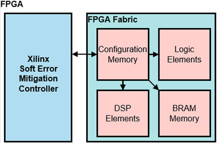
Figure 7. SEM controller: injection into configuration memory.
During fault injections, the SEM controller flips a bit in the FPGA configuration memory. For the ISS payloads, the bit was arbitrarily selected, Linear Frame Address 0x0000011, and the injection operated on a cadence of an injection every 10 s. After the injection, the SEM controller scans the ECC and CRC to find the fault. Upon the fault being found, the SEM controller attempts to correct the error using algorithmic methods (sem, 2022). This involves an active partial reconfiguration by the SEM controller on the frame containing the fault to rewrite it with the correct contents.
A Lander Analog Telemetry Test Emulator (LATTE) provided the user interface for sending commands and retrieving data packets from RadPC PCB. On RadPC PCB, the MSP430 microcontroller functioning as the MCU received commands from the LATTE and would execute those commands. On RadPC PCB, RadPC-Lunar was implemented on the FPGA, and its voter tracked tile outputs. A picture of the testing setup is shown in Figure 8. The MSP430 Launchpad and Xilinx Platform Cable, which are used to program the MCU and FPGA, respectively, are presented at the bottom of the picture. With this testing setup, the LATTE controlled the timing between injections and total number of injections per run. The MCU controlled the locations of the injections via addressing in the SEM controller’s linear-frame addressing system. The MCU also controlled packet generation for both regular data packets used in the ISS Project, labeled as FPGA, and data packets for the SEM controller’s report, labeled as SEM. On the FPGA, the SEM controller controlled the actual fault injection upon command from the MCU. Depending on the injected fault type, the SEM controller scanned the configuration memory after an injection and generated an error report that was returned to the MCU for SEM data packet generation. Moreover, on the FPGA, RadPC-Lunar was under normal operation. The voter in RadPC-Lunar was used to detect and report faults that propagated from the configuration memory into the implemented logic design. This setup allowed essential bits that caused changes in implemented logic to be differentiated from critical bits that caused detectable faults in the implemented logic design.
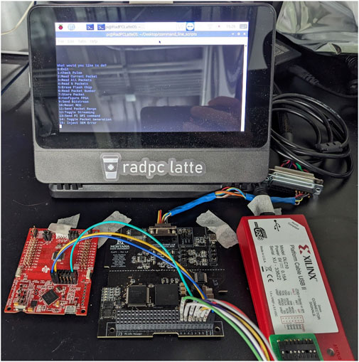
Figure 8. Configuration memory injection testing setup.
2.3.2 Error types
Two types of errors were injected during testing. The first type was designed to simulate radiation-induced faults inside the configuration memory. Single-location injections performed a bitflip at a single-address simulate radiation strikes that only acted on a single bit. The diagram of a single-fault injection for linear frame addressing is shown in Figure 9.
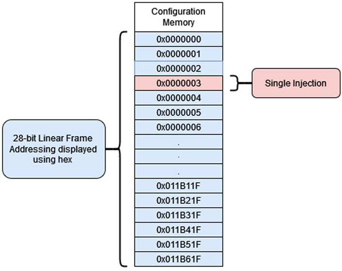
Figure 9. Single-fault injection.
After an injection, the SEM controller is set to the Observation mode to detect and repair any faults in the configuration memory. The SEM controller is capable of finding, repairing, and reporting faults within a maximum of 150 milliseconds from the start of the scan for a fault (sem, 2022). With the single-bit fault, the SEM controller is capable of an average of 23 milliseconds depending on the fault location. This particular type of fault, where only a single bit is changed, is the most likely occurrence in space operations.
The second fault type is continuous adjacent injection, as shown in Figure 10. This type of fault is unlikely to occur during space operations and was not used for simulating radiation-induced faults in the configuration memory. The purpose is to deliberately overload the configuration memory with faults, which will propagate to the implemented logic design. By comparing the locations of the continuous injections and the tile output faults from RadPC-Lunar, the general location of critical fault addresses can be found. As previously discussed in double-adjacent faults, the SEM controller is not capable of more than a single injection at a time. Between injections, the SEM controller was placed in the Idle mode to avoid it scrubbing the configuration memory and detecting the injected faults. During the time between injections, the MCU would also build data packets, indicating whether the latest continuous injection had triggered a detectable fault in RadPC-Lunar.
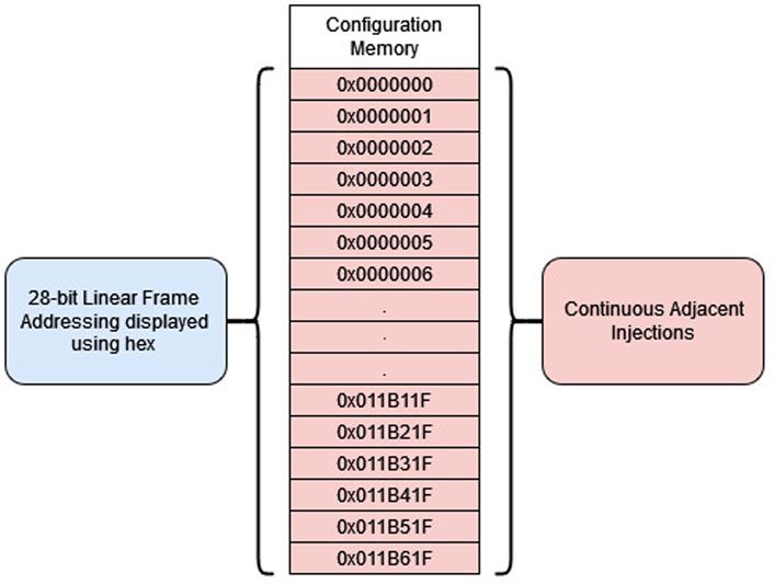
Figure 10. Continuous-fault injection.
2.3.3 Procedure for error injections
Injection consisted of the following steps. The number, type, and timing of injections were set by the user on the external test unit, the LATTE. The fault injection addresses are set by the MCU on the RadPC Rev 4.0 board. Found in the UART_A0_driver.c file, this code controls the fault injection addresses in linear frame addressing, the injection type, and the SEM controller’s state, and processes the SEM injection report returned by the FPGA into a packet. Addresses are incremented by either bits or linear frame addresses. The bits option injects at every bit location of the implemented logic system and is used for completeness in testing. The linear frame address option injects faults at the least significant bit (LSB) of each frame in the implemented logic system and is used for faster testing. After the FPGA receives the fault injection command from the MCU, it passes the command to its internal SEM controller. The SEM controller injects the fault into configuration memory via a bitflip at the given address. This fault in the configuration memory determines the behavior of the design. It describes function block behavior and function block connectivity (sem, 2022). Fifth, the SEM controller is set to either Idle or Observation. In Idle, the SEM controller allows the fault to remain in the configuration memory, thereby changing the logic system implemented on the FPGA fabric. Depending on the location of the injection, this fault can induce errors in the output of the logic system. In Observation, the SEM controller can check the ECC of the frames and the CRC codes of the arrays of frames for errors. If a fault is found, the SEM controller repairs it and returns an SEM injection report up the communication chain to the MCU, where it is stored until requested by the LATTE.
An example of a fault injection command is “IN C000000000O.” This example would inject a single fault at linear frame address “0000000,” place the SEM controller in the Observation mode to detect the fault, and have the SEM controller repair any detected errors in the FPGA’s configuration memory. After the repair, the SEM controller would generate an SEM injection report listing the classified errors by linear and physical frame addressing. This can simulate a single-event upset in configuration memory for a single bit, and delaying the SEM controller allows the length of time until a fault is repaired to be controlled.
2.3.4 Frame addressing for injections
There are two addressing schemes for fault injection into the configuration memory, namely, linear frame addressing and physical frame addressing. Linear frame addressing utilizes arbitrary addresses from 0x0000 to 0x11B6, which are mapped to the physical frame addressing of the implemented logic system.
The format for linear frame addressing is shown in Table 3. “SS” represents the hardware super logic region (SLR) number and set to “00,” and “LLLLLLLLLLLLLLLLL” represents the linear frame address (17-bit) (sem, 2022). “W W W WW WW” and “BBBBB” represent the word address (7-bit) and bit address (5-bit), respectively. The word and bit addresses are the same between linear and physical frame addressing.
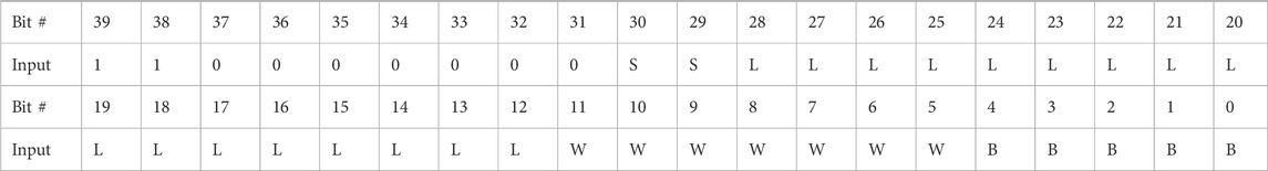
Table 3. Error injection command using linear frame addressing (sem, 2022).
Physical frame addressing utilizes the actual addresses of the implemented logic system in the FPGA’s configuration memory and is shown in Table 4. “TT” represents the block type (2-bit), “H” is the half address (1-bit), “RRRRR” is the row address (5-bit), “CCCCCCCCCC” is the column address (10-bit), and “MMMMMMM” is the minor address (7-bit) (sem, 2022). Physical frame addresses provide information on the type and physical location but are scattered across the configuration memory space to match with their physical locations in the FPGA fabric. Linear frame addressing is simpler to implement; however, the addresses do not provide type and physical location of the frame under test (sem, 2022). For the testing of the configuration memory, all addresses for the SEM injections utilize linear frame addressing. Physical frame addressing covers the entire FPGA’s configuration memory including the unutilized parts. A simulated fault may be injected into implemented elements or the unutilized FPGA elements, and Xilinx suggests using linear frame addressing for this reason (sem, 2016). As the total number of unutilized FPGA elements is approximately 33%, testing needs to be focused for time constraints. Runtimes for the SEM injections over the entire mapped linear frame addresses required 7 days at one injection per 0.25 s. Injecting over the entire memory space would require 10.5 days of runtime. As multiple runs were required for each type of fault injection, linear frame addressing was chosen for its relative speed and focused on the implemented design. Additionally, this addressing mode maps the linear frame addressing to the utilized physical frame addresses. The results pertain to simulated errors inside the design implemented on the FPGA. The physical frame address is returned within the SEM injection report for a linear frame address injection that was successfully detected and repaired. This allows physical and linear frame addresses to be cross-referenced for analysis. As the purpose of this research was to observe the effects of simulated errors inside the implemented design, only linear frame addressing was used. Physical frame addressing and testing the effects of fault injection on the entire configuration memory space are left to future research.
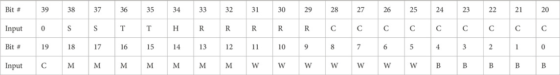
Table 4. Error injection command using linear frame addressing (sem, 2022).
2.3.5 Limitations of error injection
When interpreting the results from this experiment, there are a few key considerations. Xilinx does not support analysis of any specific customer design (sem, 2022). Tracing the fault location back to the design is not supported nor are physical locations in configuration memory matched to components in the logic design. Furthermore, Xilinx specifically states that configuration memory injection can cause the implemented logic design to behave in unpredictable ways (sem, 2016). Correlation between the SEM controller’s injections and faults in the logic design are dependent on the voter detecting the fault. As the voter is a part of the logic design, it shares the same vulnerability to configuration memory injections as the remaining RadPC-Lunar. Injections into the configuration memory defining the voter cause unpredictable multiple-tile faults.
Furthermore, injections might not be detected because many of the configuration bit locations are masked or do not exist in the actual configuration memory. For example, with RadPC-Lunar, the linear frame addresses 0x00000028 to 0x00000029 do not correspond to a valid injection address within the configuration memory. As shown in Table 5, these linear frame addresses are missing from the linear to physical address mapping. Injections at these locations return invalid injection reports. This gap appears at the edges of blocks in the configuration memory. The utilized configuration memory is divided into blocks in both linear and physical frame addressing, and the gaps appear between these blocks. The final limitation is specific to multiple bit injections. There is an undocumented time delay between injection and propagation from configuration memory to the FPGA fabric. In single-bit and double-bit injections, this is not an issue as the injections are physically close together and the fault is localized. Multiple-bit injections, such as those used for the continuous injection testing, can trigger short cascades of fault detection and correction. During these cascades, the SEM controller is continuously detecting, repairing, and reporting faults, only for the sequence to restart with new fault detection. These appear after a long series of injections and last for the next four or five reports. After this, the SEM controller recovers and continues normal operation. The current theory states that the SEM controller has an upper limit on the number of faults per report. On reaching that limit, the SEM controller sends the report and starts building another report as quickly as possible. As the SEM controller’s programming is proprietary, this theory has not been verified.
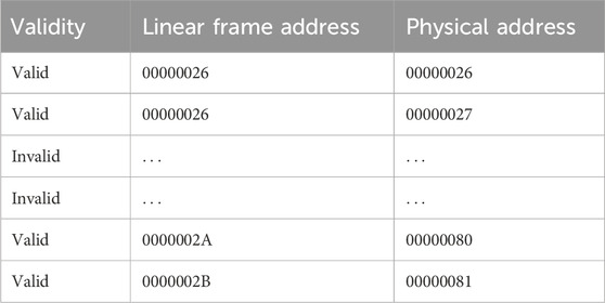
Table 5. Invalid linear frame addresses.
3 Results
Overall, RadPC-Lunar is very resistant to injections into the configuration memory. A total of 2,213,130 valid single-bit injections were performed on RadPC-Lunar over 4 months of testing, as shown in Figure 11a. Only 2.25% of these injections caused a detectable fault in the tile outputs. All the detectable errors were recoverable either through a partial reconfiguration of the faulted tile or a full reconfiguration of the whole RadPC-Lunar system.
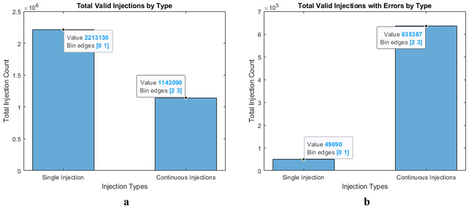
Figure 11. Total injections vs. total induced errors: (a) Total single and continuous injections and (b) total single and continuous errors.
The total number of continuous injections is also shown in Figure 11a. For this type of injection, RadPC-Lunar suffered errors for 59.52% of the total number of injections. Figure 11b shows a subset of the data from Figure 11a, where the injections resulted in errors being detected in the implemented logic design. As shown in Figure 11b, the continuous injection was more successful in causing errors in the implemented logic design. This percentage was expected as the continuous injections were specifically developed to fault RadPC-Lunar across as many components as possible.
3.1 Single-bit fault injections
In the case of single injection, the SEM controller can usually find, scrub, and report a fault without any of the tiles or voter being damaged. Table 6 shows the tile outputs and voted output of four sequential FPGA data packets. An injection was done before each of these packets was generated. The injection had no effect on the tile outputs and was either repaired before it could damage the logic design or occurred at a nonessential bit.
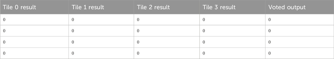
Table 6. Single-tile injection: normal operation.
The most common fault for single-injection testing is a single tile fault. As testing was conducted incrementally from the linear address 0x0000000 upward, the tile faults tended to cluster in tiles 0 and 1 as lower addresses received more coverage.
An example of a single tile fault is shown in Table 7, where Tile 1 is faulted. This error was repaired by partial reconfiguration on Tile 1. The most severe fault suffered during single-bit injection testing was a propagating double error, as shown in Table 8. This fault was originally a single fault for Tile 1, which the SEM controller successfully found and repaired. However, the following injection on the next address in the configuration memory triggered a double fault in tiles 0 and 3. As RadPC-Lunar was unable to determine which set of tiles was correct, the entire system was fully reconfigured and all tile outputs reset to zero. This error is reproducible with single injections around linear frame address 0x00001E2.
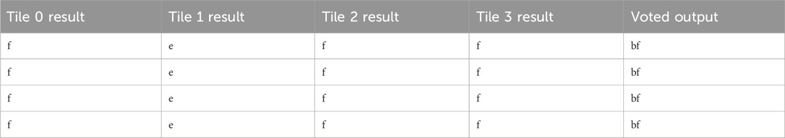
Table 7. Single injection: repairable single error.
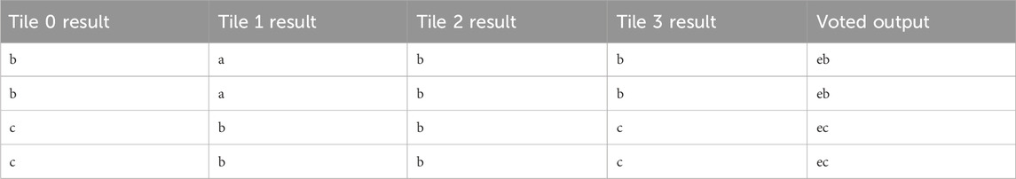
Table 8. Single injection: propagating double error.
For single-bit injections, the SEM controller coupled with RadPC-Lunar’s voter system was able to recover from the majority of faults through partial reconfiguration while maintaining operation. The remaining faults triggered a full reconfiguration to effectively restart the FPGA.
3.1.1 Continuous adjacent bit fault injection
This method of injection is an extreme test case used to identify critical bit addresses and build a linear frame address to physical frame address mapping for the entire FPGA configuration memory. An example of the linear to physical mapping is shown in Table 9. As linear frame addressing does not provide information on the physical location of logic design components, the mapping is used to convert to the physical frame. As discussed in Experiment Design, the purpose of this type of injection is not to test RadPC’s recovery capability. Instead, this injection method is designed to overwhelm the SEM controller and force repeated faults in RadPC-Lunar. These faults are biased toward the start of the address space. Continuous injections tend to cause faults at lower address numbers as entire blocks of configuration memory are overwritten.
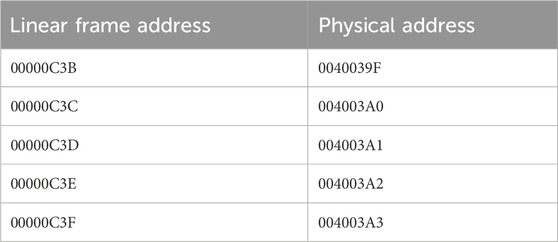
Table 9. Linear addresses to physical addresses.
Approximately 40% of injections using the continuous injection type did not cause faults. RadPC-Lunar maintained its normal operations during continuous injection testing. An example of normal tile outputs during continuous injection testing is shown in Table 10. The counter program is on its 15th loop, incrementing from 0 to F.
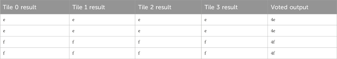
Table 10. Continuous injection: normal operation.
In the event of a single-tile fault caused by continuous injection, RadPC-Lunar was able to recover via partial reconfiguration of the affected tile. An example of faulted Tile 0 undergoing partial reconfiguration and being synchronized with the other tiles is shown in Table 11. This fault was caused by a single injection at linear frame address 0x000089E.
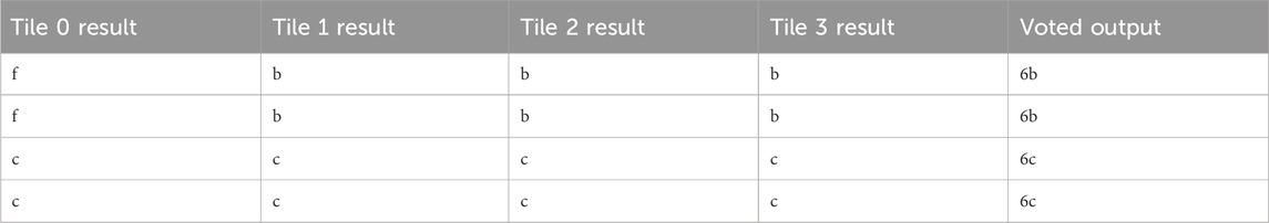
Table 11. Continuous injection: repairable single error.
An example of a single propagating error is shown in Table 12. This fault was caused by an injection at linear frame address 0x0000326. The fault propagated for 160 data packets and 12 counter increments before being detected by the voter and corrected via partial reconfiguration of Tile 0. Correlating Tile 0 output faults with the injected faults and using the linear to physical address mapping put Tile 0 between physical frame addresses 0x00000980 and 0x00020D9D in the configuration memory. Injections inside this range cause faults within Tile 0.
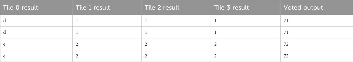
Table 12. Continuous injection: propagating single error.
The final result found using continuous injections was a multiple tile fault. This triple-tile fault requires multiple, simultaneous faults at specific locations in configuration memory to trigger three simultaneous tile faults in RadPC-Lunar. The likelihood of natural radiation bombardment causing the precise conditions required for this triple-tile fault is extremely low. Given the unlikelihood of the fault occurring under natural radiation bombardment, RadPC-Lunar is not designed to recognize these types of faults. However, the fault in Table 13 was confirmed as a triple-tile fault by cross-checking that Tile 0 was partially reconfigured and the error persisted. As a partial reconfiguration retrieves a partial bitstream from a memory chip external to the FPGA, the bitstream cannot have been altered by the SEM controller’s injections. As part of the partial reconfiguration process, the data memory scrubber uses the other three tiles’ data memory to synchronize the partial reconfigured tile. After partial reconfiguration, Tile 0 should have fully recovered. Yet on the next count, the output of Tile 0 disagrees with the other three tiles. Another partial reconfiguration is triggered. This pattern suggests that the tiles being reconfigured were actually correct, and this was a triple-tile fault.
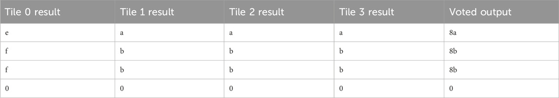
Table 13. Continuous injection: propagating triple error.
This cycle continued until the system underwent full reconfiguration and was restarted. The fault was caused by an injection, which affected the voter inputs received from tiles 1, 2, and 3. As the voter was unable to recognize a triple-tile fault, it treated this fault as a single-tile fault and partially reconfigured the uncompromised tile. The cycle described was also detected in the orbital data from the ISS, where tiles 0, 1, and 2 were all shown as correct and tile 0 was repeatedly repaired without fixing the fault.
4 Discussion
This study showed that the strategy of using Xilinx’s SEM and a microcontroller for configuration memory fault injection is viable. A number of changes are needed to meet the requirements of a systematic, comprehensive, and quick testing procedure. Injection locations need to be distributed across the entire FPGA configuration memory for systematic testing. The SEM’s fault recovery needs to be disabled during laboratory testing to allow fault propagation to the implemented logic design for verifiable results. A fault is considered to have propagated to the logic design if it is detected by the recovery subsystems inside the implemented logic design. Injection cadence needs to be reduced to allow the propagating errors to be isolated to a single injected fault. Applying these changes would allow for rapid, repeatable, and systematic testing of a Xilinx FPGA’s configuration memory using the SEM and a supervising microcontroller.
4.1 Potential radiation-induced faults in configuration memory
As discussed in the Mission Overview, RadPC functioned on the ISS for a total of 13 months between two payloads. Six uncorrectable faults were detected in the configuration memory of payload 1’s lunar board. These faults did not affect the payload’s normal operation and were removed by the next power cycle. The SEM controller is known not to cause an uncorrectable fault with its injections at linear frame address 0x0000011. The injected tile faults inside the implemented logic are also known not to cause this type of fault. This suggests that the six uncorrectable faults in the FPGA’s configuration memory were radiation-induced faults. Memory overwrites, serial communication issues, and frequent power cycles make verification difficult. Additionally, verification of the six faults being radiation-induced faults on the ground testing failed as the configuration memory testing was unable to replicate this uncorrectable fault.
4.2 Development of systematic configuration memory injection
The testing on the ground was not able to replicate the uncorrectable faults. Injections were done at all valid linear frame addresses. None of these addresses triggered a similar SEM uncorrectable fault. This suggests that the SEM uncorrectable faults were caused by faults inside the configuration memory, but outside the area, the SEM controller is allowed to inject. As Xilinx’s configuration memory design is proprietary, this hypothesis cannot be tested. However, the lack of a similar response to the permitted injections suggests that the SEM uncorrectable faults were caused by radiation. Furthermore, this research into the SEM uncorrectable faults leads to the development of a systematic configuration memory injection process for FPGA-based aerospace computers. The FPGA configuration memory on RadPC can now be systematically tested. Faults detected by the voter inside the implemented logic design can be correlated to SEM injections in the configuration memory. This development allows a new method of tile fault injection for RadPC. Currently, two separate fault injection methods are used in RadPC: one via the SEM controller for the configuration memory and another via implemented logic on the FPGA. With a map of RadPC’s responses to configuration memory injection locations, the two methods can be combined. A single injection in the configuration memory can cause a tile fault in the implemented logic design on the FPGA.
4.3 Conclusions
In conclusion, the ISS project and memory project successfully advanced the development of the RadPC aerospace computer. Radiation tolerance is a major consideration for the future of aerospace computers. RadPC provides a cost-effective, radiation-resistant system for small-satellite, data-processing applications. RadPC has been deployed to the ISS for an on-orbit test mission with two payloads. On the ISS, RadPC operated successfully for a total duration of 5 months for payload 1 and 13 months for payload 2. A number of issues, including memory overwrite, irregular communication glitches, and SEM injection cadence, were identified and resolved for future missions. Power supplies, RadPC’s recovery methods, payload response to power cycles, and payload response to natural radiation bombardment were successfully tested. At the end of the mission, RadPC payloads 1 and 2 returned to the Earth and was fully functional upon return. Furthermore, data on the on-orbit missions motivated research that developed a more robust fault injection system for configuration memory testing. The configuration memory testing showed that key components within the logic design, such as individual tiles and the voter, are particularly vulnerable to faults in the configuration memory. The voter is a particular point of vulnerability. As all the tile outputs are channeled through the voter, it is the single point of failure across the entire system. The overall system was successful in the majority of cases. Single-tile faults were successfully recovered, and propagating multiple-tile faults were recoverable through full reconfiguration of the FPGA upon MCU reset. Overall, this project successfully launched two payloads into space, where they were deployed on the ISS. Data from the ISS led to the development of a configuration memory fault injection process for FPGA-based computers.
Data availability statement
The raw data supporting the conclusions of this article is available by the authors from Montana State University at the time of writing and publication.
Author contributions
HA: Formal Analysis, Investigation, Methodology, Software, Validation, Visualization, Writing – original draft, Writing – review and editing. CM: Conceptualization, Investigation, Resources, Software, Writing – review and editing. CB: Software, Writing – review and editing. JW: Methodology, Software, Writing – review and editing. ZB: Software, Writing – review and editing. MS: Data curation, Software, Writing – review and editing. BL: Conceptualization, Funding acquisition, Methodology, Project administration, Writing – review and editing.
Funding
The author(s) declare that financial support was received for the research and/or publication of this article. This research was supported in part by NASA under award/number 80NSSC19M0037.
Conflict of interest
The authors declare that the research was conducted in the absence of any commercial or financial relationships that could be construed as a potential conflict of interest.
Generative AI statement
The author(s) declare that no Generative AI was used in the creation of this manuscript.
Publisher’s note
All claims expressed in this article are solely those of the authors and do not necessarily represent those of their affiliated organizations, or those of the publisher, the editors and the reviewers. Any product that may be evaluated in this article, or claim that may be made by its manufacturer, is not guaranteed or endorsed by the publisher.
References
AdaptiveSoC&FPGASupport (2016). 66570 - UltraScale architecture Soft error mitigation controller - guidance for testing with error injection. AMD Xilinx
Author Anonymous (2022). Soft error mitigation controller v4.1: LogiCORE IP product guide. AMD Xilinx.
Barillo, C., and Calvel, P. (1996). Review of commercial spacecraft anomalies and single-event-effect occurrences. IEEE Trans. Nucl. Sci. 43, 453–460. doi:10.1109/23.490914
Barnaby, H. J. (2006). Total-ionizing-dose effects in modern cmos technologies. IEEE Trans. Nucl. Sci. 53, 3103–3121. doi:10.1109/TNS.2006.885952
Barth, J., Dyer, C., and Stassinopoulos, E. (2003). Space, atmospheric, and terrestrial radiation environments. IEEE Trans. Nucl. Sci. 50, 466–482. doi:10.1109/TNS.2003.813131
Bedingfield, K. L., Leach, R. D., and Alexander, M. B. (1996). Spacecraft system failures and anomalies attributed to the natural space environment. NASA Reference Publication, 1390.
Benedetto, J. M., Eaton, P. H., Mavis, D. G., Gadlage, M., and Turflinger, T. (2006). Digital single event transient trends with technology node scaling. IEEE Trans. Nucl. Sci. 53, 3462–3465. doi:10.1109/TNS.2006.886044
Claeys, C., and Simoen, E. (2002). Radiation effects in advanced semiconductor materials and devices. 1 edn. Berlin, Heidelberg: Springer. doi:10.1007/978-3-662-04974-7
Ecoffet, R. (2013). Overview of in-orbit radiation induced spacecraft anomalies. IEEE Trans. Nucl. Sci. 60, 1791–1815. doi:10.1109/tns.2013.2262002
Garvie, M., and Thompson, A. (2004). “Scrubbing away transients and jiggling around the permanent: long survival of fpga systems through evolutionary self-repair,” in Proceedings. 10th IEEE international on-line testing symposium, 155–160. doi:10.1109/OLT.2004.1319674
Hughes, H. L., and Benedetto, J. M. (2003). Radiation effects and hardening of mos technology: devices and circuits. IEEE Trans. Nucl. Sci. 50, 500–521. doi:10.1109/tns.2003.812928
Jing, Z., Zengrong, L., Lei, C., Shuo, W., Zhiping, W., Lishuai, W., et al. (2012). “Study of an automated precise seu fault injection technique,” in 2012 IEEE 26th international parallel and distributed processing symposium workshops and PhD forum, 277–281. doi:10.1109/IPDPSW.2012.32
Johnston, A. (1998). Radiation effects in advanced microelectronics technologies. IEEE Trans. Nucl. Sci. 45, 1339–1354. doi:10.1109/23.685206
Joseph, E. C. (1967). Impact of large scale integration on aerospace computers. IEEE Trans. Electron. Comput. EC- 16, 558–561. doi:10.1109/PGEC.1967.264741
LaMeres, B. J. (2023). Highly integrateable AI modules for planning, scheduling, characterization, and diagnosis (ISS payload installation). Montana State University.
Liu, R., Evans, A., Chen, L., Li, Y., Glorieux, M., Wong, R., et al. (2017). Single event transient and tid study in 28 nm utbb fdsoi technology. IEEE Trans. Nucl. Sci. 64, 113–118. doi:10.1109/TNS.2016.2627015
Major, C. M., Bachman, A., Barney, C., Tamke, S., and LaMeres, B. J. (2021). Radpc: a novel single-event upset mitigation strategy for field programmable gate array–based space computing. J. Aerosp. Inf. Syst. 18, 280–288. doi:10.2514/1.I010859
Sterpone, L., and Violante, M. (2005). Analysis of the robustness of the tmr architecture in sram-based fpgas. IEEE Trans. Nucl. Sci. 52, 1545–1549. doi:10.1109/TNS.2005.856543
Yarzada, R., Singh, D., and Al-Asaad, H. (2022). “A brief survey of fault tolerant techniques for field programmable gate arrays,” in 2022 IEEE 12th annual computing and communication workshop and conference CCWC, 0823–0828. doi:10.1109/CCWC54503.2022.9720746
Zhang, C. -M., Jazaeri, F., Pezzotta, A., Bruschini, C., Borghello, G., Faccio, F., et al. (2016). “Gigarad total ionizing dose and post-irradiation effects on 28 nm bulk mosfets,” in 2016 IEEE nuclear science symposium, medical imaging conference and room-temperature semiconductor detector workshop (NSS/MIC/RTSD), 1–4. doi:10.1109/NSSMIC.2016.8069869
Keywords: configuration memory, radiation tolerance, FPGA, SEE, softcore, QMR, fault simulation
Citation: Austin H, Major C, Barney C, Williams J, Becker Z, Smith M and LaMeres B (2025) Single-event upset simulation and detection in configuration memory. Front. Space Technol. 6:1610424. doi: 10.3389/frspt.2025.1610424
Received: 12 April 2025; Accepted: 30 June 2025;
Published: 29 July 2025.
Edited by:
Changqing Xu, Xidian University, ChinaReviewed by:
Augusta Sophy Beulet P., VIT University, IndiaChang Cai, Guangzhou University, China
Tong Ye, Nanjing Vocationl University of Industry Technology, China
Gongzhe Qiao, Nanjing University of Information Science and Technology, China
Copyright © 2025 Austin, Major, Barney, Williams, Becker, Smith and LaMeres. This is an open-access article distributed under the terms of the Creative Commons Attribution License (CC BY). The use, distribution or reproduction in other forums is permitted, provided the original author(s) and the copyright owner(s) are credited and that the original publication in this journal is cited, in accordance with accepted academic practice. No use, distribution or reproduction is permitted which does not comply with these terms.
*Correspondence: Hezekiah Austin, aGV6ZWtpYWguYXVzdGluQHJlc2lsaWVudC1jb21wdXRpbmcuY29t