 J. Collado
 V. González
 J. M. Deltoro
 A. Gadea2
- 1Department of Electronic Engineering, University of Valencia, Valencia, Spain
- 2Instituto de Física Corpuscular, CSIC-Universidad de Valencia, Paterna, Spain
In nuclear and high-energy physics experiments, data acquisition systems handle vast amounts of data from thousands of detectors and electronic channels, often reaching hundreds of terabits per second. While modern field programmable gate arrays (FPGAs) offer high-speed transceivers capable of processing such data, a mismatch can arise: individual analog-to-digital converters (ADCs) process lower data rates than FPGA transceivers can efficiently handle. This inefficiency leads to unnecessary usage of more powerful and expensive FPGAs, thus increasing system costs. This paper addresses this issue by proposing a link aggregator method for ADC readout. The solution integrates five universal link aggregator devices within an FPGA mezzanine card (FMC) board, enabling 1-to-1, 2-to-1, 3-to-1, or 4-to-1 multiplexing. The system optimizes FPGA resource utilization with support for up to 40 optical or copper inputs (2.5 Gbps per link) and a 10-line aggregated output (10 Gbps max) via a Vita57.1 FMC connector. A low-cost, low-power FPGA manages the mezzanine board as an intelligent standalone device. This approach significantly reduces hardware requirements and enhances cost-efficiency in high-performance data acquisition systems.
1 Introduction
Studying exotic nuclear structures has driven the development of advanced high-resolution gamma spectrometers, such as AGATA Akkoyun et al. (2012) and EXOGAM de France (2000), which offer enhanced detection sensitivity and energy resolution. Modern nuclear physics experiments demand higher efficiencies, improved peak-to-background ratios, and complex gamma-ray tracking algorithms, leading to a shift from traditional analog front-end electronics to fully digital systems. These systems rely on high-speed analog-to-digital converters (ADCs), fast optical links, and field programmable gate array (FPGA)-based processing to manage the increasing data rates and channel densities.
A key challenge in these systems is to use as few high-speed transceivers as possible because these are very expensive. As the number of detector channels grows, additional transceivers are required. With more channels, FPGAs tend to have transceivers whose bandwidth often exceeds the capacity needed for each optical link. This results in inefficient utilization of available resources, where all transceivers are occupied despite unused bandwidth potential.
For Ethernet, there are several protocols for data aggregation, such as the port aggregation protocol (PAgP) Cisco (2006b) or the link aggregation control protocol (LACP) Cisco (2006a). However, the link aggregator solutions for ADCs are limited. Because the goal is to aggregate data from different ADCs into a single channel, we have used the TLK10022 (TexasInstruments, 2013a) device, a high-speed, dual-channel serializer/deserializer (SerDes) designed for data transmission over high-speed serial links. The TLK10022 supports data rates of up to 10 Gbps per channel. It offers low latency, high throughput, and efficient data serialization, making it suitable for applications that require robust and reliable data aggregation.
This work presents the design and implementation of the input data mezzanine (IDM) board, a hardware solution that integrates five TLK10022 to carry out data aggregation, a low-cost and low-power FPGA to lead the control and configurations, and a Vita57.1 FMC connector (Institute and Organization, 2008) with the outputs. This is a general-purpose board that aggregates low-speed channels into high-speed channels. The system has been tested and validated for the specific case of advanced gamma tracking array (AGATA) data acquisition.
The paper is organized as follows: Section 2 addresses the specific problem of AGATA, Section 3 presents the different methodologies to optimize the use of transceivers and the solution adopted; Section 4 details the design of the IDM board; Section 5 describes the validation tests performed; Section 6 presents the results obtained; and Section 7 offers the conclusions.
2 A problem: AGATA phase 2 development
The AGATA gamma-ray spectrometer is a position-sensitive crystal high-purity germanium (HPGe) detector with 180 crystal detectors projected on its final configuration to achieve a 4
Due to the complexity of the AGATA detector, it has been developed in a series of phases over time. With the ending of Phase 1 in 2020 and a goal of 45 detectors achieved, a new Phase 2 will be open until 2030 with a goal of 135 detectors. The electronics associated with Phase 1 are obsolete and subject to several improvements, such as Ethernet readout with increased bandwidth to allow the PSA analysis, online scope modes, flash ADC differential nonlinearity correction, energy extraction algorithm improvement, system integration, and global performance enhancement. This is being developed under the Phase 2 AGATA electronics, with three main goals: integrate all electronics from digitizer to readout in a single device for each crystal detector (36 segments + 2 core signals), provide a 40 Gb Ethernet readout, and enhance performance. Secondary elements to be ensured are modularity, generation compatibility, and portability.
The system integrates 100 MHz sampling rate digitizers onto the Digi-Opt12 boards, which are placed together with the preprocessing FPGA on the processing and control through ethernet - control And processing (PACE-CAP) board, equipped with a serial transfer acquisition readout over Ethernet (STARE) Ethernet mezzanine. Each of the 38 ADC data streams has a 2 Gbps bandwidth (just above the bandwidth capability of the FPGA’s regular IO pins), while the FPGA transceivers can handle up to 16.375 Gbps. The ADC data is transmitted through the JESD204B (JEDEC, 2012) interface, which allows for deterministic latency and maintaining data integrity.
Moreover, using system-on-module (SOM) modules to enhance modularity and integration further reduces the number of available FPGA transceivers. In addition to these constraints, the FPGA also manages several 10 GbE outputs and global trigger system (GTS) communication. Reducing 40 data streams of 2 Gbps to 10 data streams of 8 Gbps became a must for project development and, thus, the development in this paper.
3 Optimization methodologies
In order to compare the different solutions to approach this problem, we can calculate the bandwidth occupancy with each solution. The occupancy will be defined as follows:
Solution A: With Gigabit Transceiver High-performance (GTH)-generation transceivers for UltraScale+, the maximum bandwidth is 16.5 Gbps, while the input signal operates at 2 Gbps per channel. The occupancy per channel (Equation 1) is approximately 12.1%, assuming one channel per transceiver. Because each detector has 38 acquisition channels, 38 transceivers (one per channel) would be required to acquire all the signals.
Solution B: Increasing the number of ADCs per chip to enhance the intrinsic data rate of the JESD204B standard (JEDEC, 2012) that allows sending data in parallel. In our case, the ADC of the Digi-Opt12 (Pullia et al, 2012), ADC1413D (Pullia et al., 2014), supports up to two channels at 5 Gbps. Thus, each ADC can operate two channels at 2 Gbps. Using the PACE transceivers (16.375 Gbps), the transceiver occupancy reaches approximately 24.4%. This means that one transceiver can acquire two channels, requiring a total of 19 transceivers to capture all the signals.
Solution C: Using a link aggregator chip to perform up to 4-to-1 multiplexing. There are chips in the market capable of up to 10 Gbps multiplexing of 8-to-1 up to 1.25 Gbps input signals or 4-to-1 in up to 2.5 Gbps input signals. Some of them are TLK10081 (TexasInstruments, 2013b), TLK10002 (TexasInstruments, 2011), and TLK10022 (TexasInstruments, 2013a). The latter (TLK10022) has been chosen because it provides greater versatility and configurability than the previous ones. In our case, the streams are 2 Gbps, so only the second option is compatible with an occupancy of 48.9% and four channels per transceiver. Therefore, at least 10 transceivers are required to acquire the 38 channels.
Solution D: The last and least expensive option is to use lower-cost FPGAs to perform the multiplexing. Some small FPGAs would have about eight transceivers up to 3 Gbps (Xilinx, 2011). The occupancy will be 66.7%, but communication with the processing FPGA should be carried out through 16 GPIO ports at a lower speed. For this option, five lower-cost FPGAs are required. Because data stream synchronization is crucial, deterministic latency must be ensured, and latency studies must be performed.
Table 1 shows the occupancy of a transceiver and the number of transceivers required for each scenario.

Table 1. Transceiver occupancy for each solution and number of transceivers required for 38 signals from a single detector.
Solution C was chosen for the Phase 2 detector electronics and the board design objective. This solution is more economical than options A and B because it requires fewer transceivers, thanks to achieving greater channel aggregation. Solution D would also be more economical, but its design would be more complex.
4 The input data mezzanine board
The IDM is based on the FMC standard (Institute and Organization, 2008) and has two requirements: data aggregation and slow control tasks (monitoring and initialization). Figure 1 shows a block diagram of the IDM design with the input adapters, while Figure 2 displays an image of the physical board.
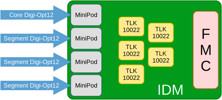
Figure 1. A diagram block of the IDM.
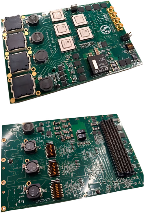
Figure 2. Top and bottom images of the first IDM prototype.
4.1 IO connectivity
Incoming data from a single Digi-Opt12 board are received through inputs linked to the IDM board via a single 9 × 9 MEG-Array connector from Amphenol (2016), as shown in Figure 1. Two connection options are available: the first uses a custom-developed board-to-board cable for a copper connection, while the second employs a four MiniPOD AFBR-822 (Avago, 2005) optical transceiver that also fits into the same connector.
When used with the optical interface option, the IDM board hosts four MiniPOD transceivers. The optical interface can be easily adapted to 12-line multi-fiber termination push-on (MTP) optical fibers or configured with multiple Lucent connector (LC) connections as needed. Therefore, 48 input channels can be input. In principle, the design foresees a maximum of 38 input channels and an input data rate of 2 Gbps per channel. The requirements demanded by AGATA electronics are met with these four MiniPODs.
4.2 The link aggregation core and configuration
The link aggregation is carried out using the Texas Instruments TLK10022 device (TexasInstruments, 2013a). This device has two channels that can merge several lines into a single line with a higher combined bitrate. The possible aggregation ratio can be configured independently for each channel. The possible ratios are 1-to-1, 2-to-1, and 4-to-1. The channel supports a maximum output bitrate of 10 Gbps and is designed to consolidate four input lines at 1 Gbps to 2.5 Gbps into a single output line ranging from 4 Gbps to 10 Gbps. It is a full-duplex device (transmission (Tx) and reception (Rx)) and can be configured to deserialize, aggregate, and reserialize the input links. The design of the IDM allows the aggregation ratio of each TLK channel to be independently configured. In our case, only data reception (Rx) is enabled, and the 4-to-1 configuration is set for all TLK channels of the IDM.
4.3 Power supply
The power supply of the IDM is sourced from the FMC connector, which provides 12 V, 3.3 V, and a variable Vadj set at 1.8 V. The 12 V input is primarily allocated for the link aggregator core and transceiver voltages. To efficiently manage power dissipation, an LTM4637 DC-DC switching regulator steps down the 12 V to 1.5 V, which then supplies four LT3070 low-dropout regulators (LDOs) to generate 1 V outputs, each capable of delivering up to 5 A. The TLK10022 transceiver requires a 1.8 V supply for its I/O, derived directly from the FMC Vadj and filtered through resistor-inductor-capacitor (RLC) networks for high-speed and low-speed transceiver power inputs. For optical links, the transceiver requires 2.5 V (max 670 mA) and 3.3 V (max 200 mA), both sourced from the FMC 3.3 V, with an LDO regulator ensuring a stable 2.5 V supply. Additionally, the FPGA requires a 1.2 V core supply (15 mA) and 3.3 V/1.8 V for its I/O, consuming less than 300 mA. These voltages are regulated from the FMC input using a DC–DC adapter, ensuring efficient power distribution across the system.
4.4 Clock distribution
The clock network in the IDM is designed to ensure precise synchronization and stability for high-speed transceivers. Given the stringent jitter requirements of the TLK10022 transceiver, which must remain below 100 ppm, a dedicated clock management section is implemented on the IDM PCB. The system synchronizes the clock signal with the FPGA RX transceiver reference clock and the digitizer sample clock of the Digi-Opt12 boards, ensuring seamless data transmission. A 200 MHz clock frequency is selected for the TLK10022 input, optimizing performance while maintaining signal integrity. Additionally, the clocking system supports selectable frequencies (even for each TLK channel) controlled through the FPGA, which accesses configuration registers via the motherboard, providing flexibility and adaptability within the system.
4.5 Slow control
The IDM board design includes a control system to automate and manage its slow control functions, overseeing initialization, setup, control, and monitoring each board element. The system also acts as an intermediary with the rest of the components. It connects all components through a single two-wire interface (TWI) bus, allowing centralized control of all devices via one controller. The core of the control is the Lattice ICE40LP4k low-power FPGA (Lattice, 2016). In this FPGA, the slow control is done autonomously. The FMC master accesses the IDM’s status information and sets alarms on important events to notify the master FMC about using an I2C protocol. In the case of a severe error, the IDM initializes itself without the master’s intervention. This I2C channel also allows for debugging tasks and fine-tuning the IDM.
The Lattice FPGA monitors all the IDM subsystems and makes useful information available to the master via a set of I2C registers. It also sends a warning if a problem arises and writes the information in local memory for possible further debugging.
4.6 The FPGA receiver firmware
As mentioned in Section 2, data transmission is carried out through the JESD204B interface. The data aggregation directly affects the JESD204B physical layer and part of the data link layer. To recover the original data, the aggregation must be inverted, and the four channels must be restored before the JESD204B encoding on the data link layer.
The incoming data have a reference clock from the IDM board phase tuned to the link aggregator Tx. Nevertheless, the mezzanines are prepared to select the desired clock for the FPGA transceivers from multiple inputs. From the transceiver’s point of view, the incoming signal is equivalent to four times the original data rate JESD204B protocol signal.
On the transmitter side, the link aggregation is done by decoding 8b10b and encoding again for the higher speed rate signal. On the receiver side, the desegregation is performed after the 8b10b and before the JESD204B decoding. The lane ordering information is obtained from an aggregator-generated mark in a K-symbol (comma) known permutation that identifies the channel 0 data. Furthermore, this part requires a clock domain change because the original JESD204B reference clock runs at a 1:4 frequency ratio with respect to the one used for the transceiver reference clock.
The JESD204B protocol is decoded by four Xilinx JESD204B IP cores per datalink, retrieving the four original digitalized data elements in the JESD204B output framework. These data have been fully tested only in JESD204B subclass 0, with no fixed latency. Nevertheless, the aggregation methodology is latency fixed, so a JESD204B subclass 1 and 2 should be possible but must be validated; the system is prepared to do so provided system and frame clock signals.
The subclass 0 of JESD204B, or JESD204A compatible, does not ensure fixed latency, leading to misaligned ADC data channels after each power-up. An optional sync pattern detector and elastic buffer have been implemented to ensure a full system alignment for up to 40 digitalized channels minimum. In order to use this functionality, a backward link from FPGA to ADC must be implemented in the system to enable the injection of a digital pattern into the ADC input signal. The selected pattern is digitalized and detected by the module, measuring the delay for each channel. The required delay is automatically applied to the elastic buffers to align all data channel sampling times.
For the JESD204B protocol to work, the sync signal must be sent to the digitizers as if no link aggregation was performed in between to ensure synchronicity. The aggregation process becomes invisible to the JESD204B actors and users as if only each single original ADC link is connected to the FPGA.
5 The validation system
The IDM board can be configured with different aggregation ratios and different clocks for each TLK channel. The testing and validation of the board have only been carried out taking into account the electronics and configuration associated with the AGATA detector.
5.1 The test bench
The test bench (See Figure 3) includes a Digi-Opt12 digitizer board with an ADC1314D sending data through JESD204B, an evaluation board TEBF0808/TE0808 evaluation board with a Xilinx Zynq Ultrascale + ZU15EV, an FMC cable extension, a workstation to control Digi-Opt12, and the IDM board under test for validation. An ATX power supply supplies the power for the evaluation board and the Digi-Opt12 custom power supply. The Digi-Opt12 is an optical output board with MTP/MPO PPOD-compatible transceivers. A patch cord adapts the MTP connection to the IDM MiniPOD.
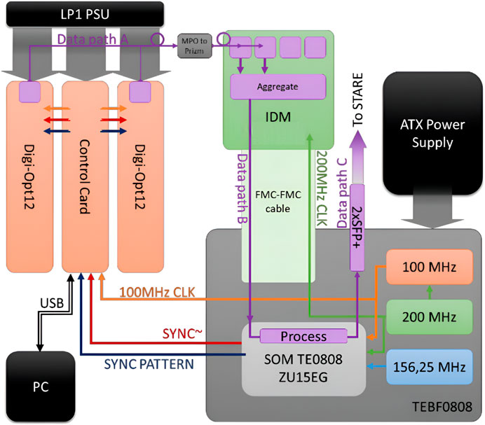
Figure 3. Test bench for IDM in the AGATA environment.
The Digi-Opt12 board can set an offset value to the differential ADC input, which must match the value read by the FPGA after the disaggregation. The incoming data will be set at a data rate of 2 Gbps and a 100 MHz sampling rate. The 4:1 aggregates data into an 8 Gbps stream fed to the FPGA Rx GTH transceivers. The ADCs work with a 100 MHz reference clock, and the aggregation and disaggregation work with a 200 MHz reference clock; both are phase-aligned.
5.2 Data path validation
Because the entire channel is very long and can lead to complex errors when combined, it was decided to test the data path separately. This approach simplifies the testing process and makes it easier to identify and correct errors, as each data path corresponds to a unique communication link and can be verified independently.
The test bench establishes three essential connections for the data paths:
• Data Path A: Connecting the Digi-Opt12 transceivers to the IDM prototype transceivers and the TLK10022.
• Data Path B: Linking the TLK10022 to the motherboard FPGA.
• Data Path C: Extending from the motherboard to the STARE 10 Gbps Ethernet.
These connections enable comprehensive testing across the various data paths. The IDM prototype’s validation primarily targeted data paths A and B, while the full data chain test initially focused on data path C.
6 Results
6.1 Path A and B preliminary test
A pseudo-random PRBS7 signal is generated from the ADC on the Digi-Opt12 to validate data path A, which is then received and validated by the TLK. Additionally, thanks to the test point connected to the loss-of-signal pin of the optical transceiver, it has been confirmed that the optical signal reaches all channels correctly, indicating an active optical signal.
Data path B was validated using PRBS7 and PRBS31 signals generated by the TLK10022, with the FPGA analyzing eye diagrams and bit error rate (BER) via an Xilinx integrated bit error ratio tester (IBERT). The GTH Rx transceivers detected pseudo-andom binary sequence (PRBS) patterns without errors, and eye diagrams showed a 71% eye opening at 2 Gbps, reducing to 50% at 8 Gbps. Data transmission used 8b/10b coding and JESD204B alignment after PRBS tests. Aggregation was verified through stable transmission to the SOM board, with lane alignment patterns identifying errors. Despite measurement limitations, the oscilloscope confirmed an open eye at 8 Gbps. Jitter analysis showed high periodic jitter due to data-dependent jitter from inter-symbol interference, but overall signal integrity remained acceptable with low cross talk.
6.2 The link performance and data recovery
A full data chain test validated the capability of AGATA Phase 2 electronics to transmit ADC data via Ethernet, meeting key design goals. Using the STARE Ethernet board and a KCU105 evaluation board with Kintex Ultrascale XCKU040 FPGA, stable data transmission was achieved at 9 Gbps and 5 Gbps between the preprocessing SOM module and a workstation server. Data encoded in the JESD204B format were transmitted error-free over a 10 Gbps Aurora link, first in internal loopback and then through optical fibers for external loopback, simulating the AGATA ADC link.
The testbench integrated the IDM and STARE prototypes, connected via an SFP + OM3 cable. Data generated by the PACE SOM in JESD204B format (32-bit counter at 50 MHz) were transmitted and received without errors. External loopback tests verified data integrity at 1.6 Gbps, with throughput reaching 3.2 Gbps under double-rate conditions. Aggregated channels demonstrated the potential to scale to 9–10 Gbps, confirming the system’s ability to handle high data rates while optimizing FPGA resources.
This successful data chain test demonstrates the viability of AGATA Phase 2’s Ethernet-based readout solution, paving the way for the pre-production phase.
7 Conclusion
This paper presents an effective solution for optimizing bandwidth in high-speed ADC-to-FPGA communication. By implementing a board to aggregate channels, we demonstrated a reduction in FPGA transceiver usage while maximizing bandwidth utilization.
The proposed IDM board, featuring the TLK10022 link aggregator and slow control automation via a Lattice FPGA, successfully aggregates 2 Gbps ADC signals into higher-rate 8 Gbps links, reducing transceiver demands and improving overall efficiency. Validation through extensive testing confirmed stable data transmission, effective synchronization, and robust performance under the JESD204B interface. This work optimizes FPGA resources and establishes a scalable, cost-effective approach for high-performance data acquisition systems. The design is foreseen for an experimental nuclear application but could be used in any generic application where low-cost data aggregation would be needed.
Data availability statement
The original contributions presented in the study are included in the article/supplementary material; further inquiries can be directed to the corresponding author.
Author contributions
JC: conceptualization, investigation, methodology, validation, writing – original draft, and writing – review and editing. VG: funding acquisition, resources, supervision, and writing – review and editing. JD: conceptualization, supervision, visualization, and writing – review and editing. AG: funding acquisition, investigation, resources, supervision, and writing – review and editing.
Funding
The author(s) declare that financial support was received for the research and/or publication of this article. Work partially funded by FEDER/MICIU-AEI with grants FPA2017-84756-C4-4-P and FPA2017-84756-C4-1-P and MICIU MCIN/AEI/10.13039/501100011033, Spain, with grant PID2020-118265GB-C42,-C44.
Conflict of interest
The authors declare that the research was conducted in the absence of any commercial or financial relationships that could be construed as a potential conflict of interest.
Generative AI statement
The author(s) declare that no Generative AI was used in the creation of this manuscript.
Publisher’s note
All claims expressed in this article are solely those of the authors and do not necessarily represent those of their affiliated organizations, or those of the publisher, the editors and the reviewers. Any product that may be evaluated in this article, or claim that may be made by its manufacturer, is not guaranteed or endorsed by the publisher.
References
Akkoyun, S., Algora, A., Alikhani, B., Ameil, F., de Angelis, G., Arnold, L., et al. (2012). Agata—advanced gamma tracking array. Nucl. Instrum. Methods Phys. Res. Sect. A Accel. Spectrom. Detect. Assoc. Equip. 668, 26–58. doi:10.1016/J.NIMA.2011.11.081
Amphenol (2016). Meg-array® — mezzanine connectors — amphenol. Available online at: https://www.amphenol-cs.com/product-series/meg-array.html# (Accessed February 11, 2025).
Avago (2005). Afbr-800evk minipod evaluation kit and afbr-800evb minipod evaluation board product brief. Available online at: https://docs.broadcom.com/doc/AV02-2843EN_PB_AFBR-800EVK_2012-06-18 (Accessed February 11, 2025).
Cisco (2006a). Link aggregation control protocol (lacp). 3ad - cisco 802. Available online at: https://www.cisco.com/c/en/us/td/docs/ios/12_2sb/feature/guide/gigeth.html (Accessed February 05, 2025).
Cisco (2006b). Port aggregation protocol cisco. Available online at: https://www.cisco.com/c/dam/en/us/td/docs/switches/lan/catalyst9600/software/release/16-12/configuration_guide/lyr2/configuring_etherchannels.html#port-aggregation-protocol (Accessed February 11, 2025).
de France, G (2000). Exogam detectors. Available online at: https://www.ganil-spiral2.eu/scientists/ganil-spiral-2-facilities/instrumentation/exogam/(Accessed February 05, 2025).
Institute, A. N. S., and Organization, V. S. (2008). ANSI-VITA 57.1-2008: American national standard for FPGA mezzanine card (FMC) standard (VMEbus International Trade Association)
JEDEC (2012). Serial interface for data converters - jesd204b. Available online at: https://www.jedec.org/sites/default/files/docs/JESD204B.pdf.
Lattice (2016). ice40 lp/hx — low power, high performance fpga. Available online at: https://www.latticesemi.com/ice40 (Accessed February 11, 2025).
Pullia, A., Barrientos, D., Bazzacco, D., Bellato, M., Bortolato, D., and Isocrate, R. (2012). A 12-channel 14/16-bit 100/125-ms/s digitizer with 24-gb/s optical output for agata/galileo. IEEE Nuclear Science Symposium Conference Record, 819–823doi. doi:10.1109/NSSMIC.2012.6551218
Pullia, A., Barrientos, D., Bazzacco, D., Bellato, M., and Recchia, F. (2014). Using analog-to-digital converter adc1413d for high-resolution gamma-ray spectroscopy. 2014 IEEE Nucl. Sci. Symposium Med. Imaging Conf. (NSS/MIC), 1–3. doi:10.1109/NSSMIC.2014.7431137
TexasInstruments (2011). Tlk10002 data sheet, product information and support — ti. com. Available online at: https://www.ti.com/product/TLK10002 (Accessed February 11, 2025).
TexasInstruments (2013a). Tlk10022 data sheet, product information and support — ti. com. Available online at: https://www.ti.com/product/TLK10022 (Accessed February 11, 2025).
TexasInstruments (2013b). Tlk10081 data sheet, product information and support — ti. com. Available online at: https://www.ti.com/product/TLK10081 (Accessed February 11, 2025).
Xilinx (2011). Spartan 6 fpgas. Available online at: https://www.amd.com/es/products/adaptive-socs-and-fpgas/fpga/spartan-6.html (Accessed March 10, 2025).
Keywords: FPGA data transfer, optical fiber networks, sensor arrays, time division multiplexing, HPGe spectrometry
Citation: Collado J, González V, Deltoro JM and Gadea A (2025) High-speed ADC-to-FPGA communication bandwidth optimization with link aggregator. Front. Detect. Sci. Technol. 3:1544824. doi: 10.3389/fdest.2025.1544824
Received: 13 December 2024; Accepted: 28 March 2025;
Published: 25 April 2025.
Edited by:
Cristina Fernández Bedoya, Centro de Investigaciones Energéticas, Medioambientales y Tecnológicas, SpainReviewed by:
Paolo De Remigis, INFN, ItalyÁlvaro Navarro, Centro de Investigaciones Energéticas, Medioambientales y Tecnológicas, Spain
Copyright © 2025 Collado, González, Deltoro and Gadea. This is an open-access article distributed under the terms of the Creative Commons Attribution License (CC BY). The use, distribution or reproduction in other forums is permitted, provided the original author(s) and the copyright owner(s) are credited and that the original publication in this journal is cited, in accordance with accepted academic practice. No use, distribution or reproduction is permitted which does not comply with these terms.
*Correspondence: J. M. Deltoro, am9zZS5tLmRlbHRvcm9AaWZpYy51di5lcw==