 V. Stanishev
 I. Streicher
 A. Papamichail
 V. Rindert1
 P. P. Paskov
 S. Leone
- 1NanoLund, Center for III-Nitride Technology, C3NiT - Janzén, Terahertz Materials Analysis Center, THeMAC, and Solid State Physics Division, Lund University, Lund, Sweden
- 2Terahertz Materials Analysis Center, THeMAC and Center for III-Nitride technology C3NiT - Janzén, Department of Physics, Chemistry and Biology, (IFM), Linköping University, Linköping, Sweden
- 3Fraunhofer Institute for Applied Solid State Physics IAF, Freiburg, Germany
- 4Consiglio Nazionale delle Ricerche - Istituto per la Microelettronica e Microsistemi (CNR-IMM), Catania, Italy
We present a contactless determination of the two-dimensional electron gas (2DEG) properties in AlScN/GaN and AlYN/GaN high electron mobility transistor (HEMT) structures using the terahertz optical Hall effect (OHE) over a temperature range of 20 K–360 K. The structures are grown on sapphire or 4H-SiC substrates by metalorganic chemical vapor deposition (MOCVD) and feature ∼10-nm thick barrier layers with Sc and Y contents ranging from 4.6% to 17.3% and 3.3% to 8.2%, respectively. The temperature dependencies of the 2DEG density and mobility parameters are analyzed and discussed in a comparative manner. Additionally, conclusions are drawn regarding the predominant scattering mechanisms at both low and room temperatures. Furthermore, the 2DEG effective mass parameter
1 Introduction
In recent decades, GaN-based technology has not only revolutionized solid-state lighting and optoelectronics but has also emerged as a key enabler of a more sustainable future, driving the development of high-efficiency radio-frequency and high-power electronic devices (Amano et al., 2018). Achieving this potential relies on the advancement of high-power transistors capable of switching large currents at high frequencies and across wide bandwidths. In this context, AlGaN/GaN high-electron-mobility transistors (HEMTs) have proven particularly promising, with commercially available devices already meeting these demanding performance requirements (Quay et al., 2017; Ture et al., 2019; Cwiklinski et al., 2019; 2020; Meneghini et al., 2021; Roccaforte et al., 2018; Krause et al., 2023).
In AlGaN/GaN HEMTs, electrons accumulate at the interface between the GaN channel layer and the AlGaN barrier due to the different bandgap energies as well as the spontaneous and piezoelectric polarizations inherent to these wurtzite nitride layers (Ambacher et al., 1999; Ture et al., 2019; Cwiklinski et al., 2019; 2020; Thome et al., 2022; Fichtner et al., 2024). These electrons are confined close to the interface, forming a two-dimensional electron gas (2DEG) with very high electron mobilities. The higher the 2DEG density
One approach to improve the performance of GaN-based HEMTs is to use the novel nitride semiconductors AlScN and AlYN as barrier layers. These materials have large bandgaps and intrinsically high spontaneous polarization, which allows for an enhanced
AlScN/GaN and AlYN/GaN heterostucture grown by molecular beam epitaxy (MBE) exhibit characteristics superior to those of conventional low-Al content AlGaN/GaN heterostructures (Hardy et al., 2017; Frei et al., 2019; Elias et al., 2023; Wang et al., 2023a,c,b; Hasan et al., 2024) and demonstrated the viability of utilizing AlScN and AlYN as barrier layers in GaN-based HEMTs. However, MOCVD is the preferred growth technique in industry because of its higher throughput, lower cost, and faster growth processes. On the other hand, the growth of AlScN and AlYN by MOCVD is challenging due to the low vapor pressure of available Sc and Y precursors. A heated gas mixing system was recently demonstrated at Fraunhofer IAF, enabling MOCVD growth with precursors that have extremely low vapor pressures. This advancement facilitated the successful growth of the first AlScN (Leone et al., 2020) and AlYN (Leone et al., 2023) by MOCVD, as well as AlScN/GaN (Streicher et al., 2023a; Leone et al., 2020; Ligl et al., 2020; Manz et al., 2021; Streicher et al., 2023b; 2024a) and AlYN/GaN (Streicher et al., 2024b) heterostructures with the presence of a 2DEG.
Optimization and further improvement of AlScN/GaN and AlYN/GaN HEMTs require accurate assessment of 2DEG properties and scattering mechanisms. Traditionally, charge carrier mobility
In this work we report a study of the temperature-dependent 2DEG properties in MOCVD grown AlScN/GaN and AlYN/GaN HEMT structures by using the contactless THz OHE.
2 Materials and methods
2.1 Samples
The AlScN/GaN and AlYN/GaN heterostructures were grown by MOCVD as described in Streicher et al. (2024a) and Streicher et al. (2024b). Thick GaN channel layers (
2.2 OHE measurements
OHE measurements were carried out at the terahertz (THz) wavelength range to study the 2DEG properties in the AlScN/GaN and AlYN/GaN HEMT structures. The OHE describes the magnetic field-induced optical birefringence generated by free charge carriers under the influence of the Lorentz force and can be measured by Mueller matrix spectroscopic ellipsometry (Schubert et al., 2016). The Mueller matrix,
with
In this study, we used the THz cavity-enhanced optical Hall effect (CE-OHE) technique, where a fully reflective aluminum surface is placed behind the sample with a small gap of about 100
2.3 OHE data analysis
The THz ellipsometer is of rotating analyzer type, which allows one to measure only the upper left
The 2DEG is described as a thin layer of Drude-type carriers in the presence of a magnetic field (Schubert et al., 2016; Kühne et al., 2018). The parameters describing the properties of the 2DEG, the carrier mobility
Figure 1 shows an example of CE-OHE measurements performed at room temperature and magnetic fields
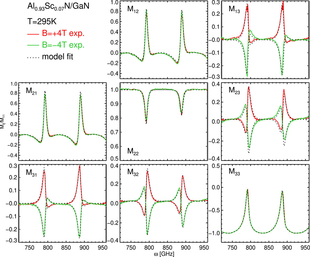
Figure 1. Representative THz OHE Mueller Matrix spectra measured at magnetic field
3 Results and discussion
Figure 2 shows the results of a series of three
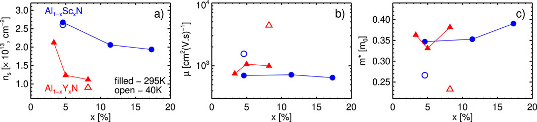
Figure 2. (a) 2DEG density,
For two of the HEMTs on sapphire, one AlScN/GaN and one AlYN/GaN, OHE measurements at
To further study the dependence of the 2DEG parameters on temperature, two HEMT samples grown on 4H-SiC substrates with 7% Sc and 5% Y in the barrier layers were selected. Figure 3 shows the 2DEG density
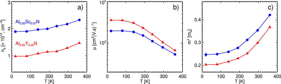
Figure 3. (a) 2DEG density
The mobility parameter exhibits a typical trend, increasing as temperature decreases before saturating below 100 K (Figure 3b). For all temperatures, the 2DEG mobility in AlYN/GaN remains higher than in AlScN/GaN, reaching
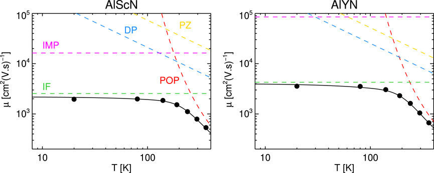
Figure 4. Best fits to the mobility data vs. temperature for
Figures 2c, 3c show that at low temperatures (bellow
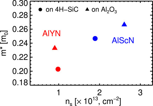
Figure 5. Low temperature effective mass parameter as function of the 2DEG sheet carrier density. Note that AlScN/GaN and AlYN/GaN samples grown on both sapphire/GaN (40 K) and 4H-SiC (20 K) are shown.
Another cause of effective mass increase could be associated with the polaronic effect. The quasiparticle polaron is used to describe the interaction (coupling) of free charge carriers with the lattice vibrations, phonons. The formation of polarons decreases the carriers mobility and increases their effective mass. As the phonon population increases with increasing temperature, the polaronic effect is expected to be enhanced at RT and higher. This process is responsible for the reduction of carrier mobility at high temperatures (Figure 4). In the case of 2DEG weakly interacting with phonons in the surrounding 3D media, the relation between the effective mass of the polaron
where
Armakavicius et al. (2024a) discussed the possibility that the free-electron behavior deviates from the classical Drude model. One set of models introduces the so-called memory functions (Götze and Wölfle, 1972; Zwanzig, 1961; Mori, 1965). In some implementations of this model, the effective mass parameter becomes a function of both frequency and temperature (Rukelj, 2020; Kumari and Singh, 2020; Kupčić, 2017), and could potentially explain our results. However, analytical expressions for semiconductors have not been developed, and quantitative evaluation of these models is currently not straightforward.
Recently, Korotyeyev et al. (2022) proposed that deviations from the classical Drude model–arising from thermally activated inelastic electron scattering processes–could qualitatively explain the increase in the effective mass parameter with temperature in AlGaN/GaN with grating couplers as reported by Pashnev et al. (2020). According to Korotyeyev et al. (2022), their model, which accounts for inelastic scattering, requires only an 18% enhancement of the effective mass at room temperature to fit the experimental data of Pashnev et al. (2020), in contrast to the
Finally, it should be noted that some earlier works on thick GaN layers, have reported effective mass at room temperature
Because the effective mass can be most easily directly measured through cyclotron resonance at low temperatures, the polaronic, non-parabolicity, and other effects on the effective mass parameters at high temperature are not well studied experimentally and thus the existing theoretical models have not been rigorously tested. The recent development of the OHE made it possible for the first time to directly access the effective mass parameter at temperatures above RT and evidence for the increase of the effective mass parameter with temperature in GaN based materials has began to emerge. We have discussed several possible mechanisms that could partially explain this. While we are currently not in a position to conclusively identify quantitatively the process (or a combination of processes) responsible for the strong dependence of the effective mass parameter on temperature, we hope that our findings will stimulate further theoretical and experimental investigations on this subject. It would also be interesting to perform similar studies on other materials that are not GaN-based.
4 Conclusion
The 2DEG density, mobility, and effective mass parameters in AlScN/GaN and AlYN/GaN HEMTs have been determined using THz optical Hall effect measurements over a temperature range of 20 K–360 K. At room temperature, the AlScN heterostructures exhibit a 2DEG sheet density
Data availability statement
The raw data supporting the conclusions of this article will be made available by the authors, without undue reservation.
Author contributions
VS: Visualization, Writing – review and editing, Formal Analysis, Writing – original draft, Investigation, Conceptualization. IS: Writing – review and editing, Investigation, Resources. AP: Investigation, Writing – review and editing. VR: Writing – review and editing, Investigation. PP: Writing – review and editing, Investigation. SL: Supervision, Investigation, Resources, Writing – review and editing. VD: Supervision, Funding acquisition, Resources, Conceptualization, Writing – review and editing.
Funding
The author(s) declare that financial support was received for the research and/or publication of this article. This work is supported by the Swedish Governmental Agency for Innovation Systems VINNOVA under the Competence Center Program (Grant No. 2022-03139), by Knut and Alice Wallenberg Foundation funded grant ‘Transforming ceramics into next-generation semiconductors’ (Grant No. 2024.0121), by the Swedish Research Council (VR) under Grant No. 2023-04993 and by the Swedish Government Strategic Research Area NanoLund. V.D. acknowledges support by the Knut and Alice Wallenberg Foundation for a Scholar award (Grant No. 2023.0349).
Conflict of interest
The authors declare that the research was conducted in the absence of any commercial or financial relationships that could be construed as a potential conflict of interest.
The author(s) declared that they were an editorial board member of Frontiers, at the time of submission. This had no impact on the peer review process and the final decision.
Generative AI statement
The author(s) declare that no Generative AI was used in the creation of this manuscript.
Publisher’s note
All claims expressed in this article are solely those of the authors and do not necessarily represent those of their affiliated organizations, or those of the publisher, the editors and the reviewers. Any product that may be evaluated in this article, or claim that may be made by its manufacturer, is not guaranteed or endorsed by the publisher.
References
Adamov, R. B., Pashnev, D., Shalygin, V. A., Moldavskaya, M. D., Vinnichenko, M. Y., Janonis, V., et al. (2021). Optical performance of two dimensional electron gas and GaN:C buffer layers in AlGaN/AlN/GaN heterostructures on SiC substrate. Appl. Sci. 11, 6053. doi:10.3390/app11136053
Amano, H., Baines, Y., Beam, E., Borga, M., Bouchet, T., Chalker, P. R., et al. (2018). The 2018 GaN power electronics roadmap. J. Phys. D Appl. Phys. 51, 163001. doi:10.1088/1361-6463/aaaf9d
Ambacher, O., Christian, B., Yassine, M., Baeumler, M., Leone, S., and Quay, R. (2021). Polarization induced interface and electron sheet charges of pseudomorphic ScAlN/GaN, GaAlN/GaN, InAlN/GaN, and InAlN/InN heterostructures. J. Appl. Phys. 129, 204501. doi:10.1063/5.0049185
Ambacher, O., Smart, J., Shealy, J. R., Weimann, N. G., Chu, K., Murphy, M., et al. (1999). Two-dimensional electron gases induced by spontaneous and piezoelectric polarization charges in N- and Ga-face AlGaN/GaN heterostructures. J. Appl. Phys. 85, 3222–3233. doi:10.1063/1.369664
Armakavicius, N., Chen, J.-T., Hofmann, T., Knight, S. K., ̆hne, P., Nilsson, D., et al. (2016). Properties of two-dimensional electron gas in AlGaN/GaN HEMT structures determined by cavity-enhanced THz optical Hall effect. Phys. status solidi C. 13, 369–373. doi:10.1002/pssc.201510214
Armakavicius, N., Knight, S., Kühne, P., Stanishev, V., Tran, D. Q., Richter, S., et al. (2024a). Electron effective mass in GaN revisited: new insights from terahertz and mid-infrared optical Hall effect. Apl. Mater. 12, 021114. doi:10.1063/5.0176188
Armakavicius, N., Kühne, P., Papamichail, A., Zhang, H., Knight, S., Persson, A., et al. (2024b). Electronic properties of group-III nitride semiconductors and device structures probed by THz optical Hall effect. Materials 17, 3343. doi:10.3390/ma17133343
Cai, D., Chen, X., Xu, H., Lin, N., Xu, F., and Chen, H. (2013). Abruptness improvement of the interfaces of AlGaN/GaN superlattices by cancelling asymmetric diffusion. Jpn. J. Appl. Phys. 52, 08JB30. doi:10.7567/JJAP.52.08JB30
Casamento, J., Nguyen, T.-S., Cho, Y., Savant, C., Vasen, T., Afroz, S., et al. (2022). Transport properties of polarization-induced 2D electron gases in epitaxial AlScN/GaN heterojunctions. Appl. Phys. Lett. 121, 192101. doi:10.1063/5.0108475
Cwiklinski, M., Brückner, P., Leone, S., Friesicke, C., Lozar, R., Maßler, H., et al. (2019). “190-GHz G-band GaN amplifier MMICs with 40GHz of bandwidth,” in 2019 IEEE MTT-S international microwave symposium (IMS), 1257–1260. doi:10.1109/MWSYM.2019.8700762
Cwiklinski, M., Brückner, P., Leone, S., Krause, S., Friesicke, C., Maßler, H., et al. (2020). “First demonstration of G-band broadband GaN power amplifier MMICs operating beyond 200 GHz,” in 2020 IEEE/MTT-S international microwave symposium (IMS), 1117–1120. doi:10.1109/IMS30576.2020.9224041
del Alamo, J. A., and Lee, E. S. (2019). Stability and reliability of lateral GaN power field-effect transistors. IEEE Trans. Electron Devices 66, 4578–4590. doi:10.1109/TED.2019.2931718
Devreese, J. T., and Peeters, F. M. (1987). “Electron-phonon interaction in two-dimensional systems: polaron effects and screening,” in The physics of the two-dimensional electron gas. Editors J. T. Devreese, and F. M. Peeters (Boston, MA: Springer US), 131–182. doi:10.1007/978-1-4613-1907-8_5
Dinh, D. V., Lähnemann, J., Geelhaar, L., and Brandt, O. (2023). Lattice parameters of ScxAl1−xN layers grown on GaN(0001) by plasma-assisted molecular beam epitaxy. Appl. Phys. Lett. 122, 152103. doi:10.1063/5.0137873
Dogmus, E., Kabouche, R., Lepilliet, S., Linge, A., Zegaoui, M., Ben-Ammar, H., et al. (2016). InAlGaN/GaN HEMTs at cryogenic temperatures. Electronics 5, 31. doi:10.3390/electronics5020031
Elias, C., Nemoz, M., Rotella, H., Georgi, F., Vézian, S., Hugues, M., et al. (2023). Influence of the temperature on growth by ammonia source molecular beam epitaxy of wurtzite phase ScAlN alloy on GaN. Apl. Mater. 11, 031105. doi:10.1063/5.0139588
Fedyanin, V. K., and Rodriguez, C. (1982a). Path integral approach to polaron mass and radius at finite temperatures. Phys. A Stat. Mech. its Appl. 112, 615–630. doi:10.1016/0378-4371(82)90200-X
Fedyanin, V. K., and Rodriguez, C. (1982b). Temperature and coupling strength dependence of polaron effective mass and radius. Phys. status solidi (b) 110, 105–113. doi:10.1002/pssb.2221100112
Feneberg, M., Lange, K., Lidig, C., Wieneke, M., Witte, H., Bläsing, J., et al. (2013). Anisotropy of effective electron masses in highly doped nonpolar GaN. Appl. Phys. Lett. 103, 232104. doi:10.1063/1.4840055
Fichtner, S., Yassine, M., Van de Walle, C. G., and Ambacher, O. (2024). Clarification of the spontaneous polarization direction in crystals with wurtzite structure. Appl. Phys. Lett. 125, 040501. doi:10.1063/5.0217301
Frei, K., Trejo-Hernández, R., Schütt, S., Kirste, L., Prescher, M., Aidam, R., et al. (2019). Investigation of growth parameters for ScAlN-barrier HEMT structures by plasma-assisted MBE. Jpn. J. Appl. Phys. 58, SC1045. doi:10.7567/1347-4065/ab124f
Fu, K., Fu, H., Deng, X., Su, P.-Y., Liu, H., Hatch, K., et al. (2021). The impact of interfacial Si contamination on GaN-on-GaN regrowth for high power vertical devices. Appl. Phys. Lett. 118, 222104. doi:10.1063/5.0049473
Fu, K., Fu, H., Liu, H., Alugubelli, S. R., Yang, T.-H., Huang, X., et al. (2018). Investigation of GaN-on-GaN vertical p-n diode with regrown p-GaN by metalorganic chemical vapor deposition. Appl. Phys. Lett. 113, 233502. doi:10.1063/1.5052479
Götze, W., and Wölfle, P. (1972). Homogeneous dynamical conductivity of simple metals. Phys. Rev. B 6, 1226–1238. doi:10.1103/PhysRevB.6.1226
Hardy, M. T., Downey, B. P., Nepal, N., Storm, D. F., Katzer, D. S., and Meyer, D. J. (2017). (Invited) ScAlN: a novel barrier material for high power GaN-based rf transistors. ECS Trans. 80, 161–168. doi:10.1149/08007.0161ecst
Hasan, M. T., Liu, J., Wang, D., Mondal, S., Tanim, M. M. H., Yang, S., et al. (2024). Effect of temperature on the performance of ScAlN/GaN high-electron mobility transistor. Appl. Phys. Lett. 125, 213503. doi:10.1063/5.0239643
Hofmann, T., Kühne, P., Schoeche, S., Chen, J.-T., Forsberg, U., Janzen, E., et al. (2012). Temperature dependent effective mass in AlGaN/GaN high electron mobility transistor structures. Appl. Phys. Lett. 101. doi:10.1063/1.4765351
Jena, D. (2022). Quantum physics of semiconductor materials and devices. Oxford University Press. doi:10.1093/oso/9780198856849.001.0001
Kasic, A., Schubert, M., Einfeldt, S., Hommel, D., and Tiwald, T. E. (2000). Free-carrier and phonon properties of n- and p-type hexagonal GaN films measured by infrared ellipsometry. Phys. Rev. B 62, 7365–7377. doi:10.1103/PhysRevB.62.7365
Kazior, T. E., Chumbes, E. M., Schultz, B., Logan, J., Meyer, D. J., and Hardy, M. T. (2019). “High power density ScAlN-based heterostructure FETs for mm-wave applications,” in 2019 IEEE MTT-S international microwave symposium (IMS), 1136–1139. doi:10.1109/MWSYM.2019.8701055
Knight, S., Richter, S., Papamichail, A., Kühne, P., Armakavicius, N., Guo, S., et al. (2023). Room temperature two-dimensional electron gas scattering time, effective mass, and mobility parameters in AlxGa1−xN/GaN heterostructures (0.07 ≤ x ≤ 0.42). J. Appl. Phys. 134, 185701. doi:10.1063/5.0163754
Knight, S., Schöche, S., Kühne, P., Hofmann, T., Darakchieva, V., and Schubert, M. (2020). Tunable cavity-enhanced terahertz frequency-domain optical Hall effect. Rev. Sci. Instrum. 91, 083903. doi:10.1063/5.0010267
Korotyeyev, V. V., Kochelap, V. A., Kaliuzhnyi, V. V., and Belyaev, A. E. (2022). High-frequency conductivity and temperature dependence of electron effective mass in AlGaN/GaN heterostructures. Appl. Phys. Lett. 120, 252103. doi:10.1063/5.0093292
Krause, S., Streicher, I., Waltereit, P., Kirste, L., Brückner, P., and Leone, S. (2023). AlScN/GaN HEMTs grown by metal-organic chemical vapor deposition with 8.4 W/mm output power and 48% power-added efficiency at 30 GHz. IEEE Electron Device Lett. 44, 17–20. doi:10.1109/LED.2022.3220877
Kühne, P., Armakavicius, N., Stanishev, V., Herzinger, C. M., Schubert, M., and Darakchieva, V. (2018). Advanced terahertz frequency-domain ellipsometry instrumentation for in situ and ex situ applications. IEEE Trans. Terahertz Sci. Technol. 8, 257–270. doi:10.1109/TTHZ.2018.2814347
Kumari, K., and Singh, N. (2020). The memory function formalism: an overview. Eur. J. Phys. 41, 053001. doi:10.1088/1361-6404/ab9931
Kupčić, I. (2017). Intraband memory function and memory-function conductivity formula in doped graphene. Phys. Rev. B 95, 035403. doi:10.1103/PhysRevB.95.035403
Leone, S., Ligl, J., Manz, C., Kirste, L., Fuchs, T., Menner, H., et al. (2020). Metal-Organic chemical vapor deposition of aluminum scandium nitride. Phys. status solidi (RRL) – Rapid Res. Lett. 14, 1900535. doi:10.1002/pssr.201900535
Leone, S., Streicher, I., Prescher, M., Straňàk, P., and Kirste, L. (2023). Metal-Organic chemical vapor deposition of aluminum yttrium nitride. Phys. status solidi (RRL) – Rapid Res. Lett. 17, 2300091. doi:10.1002/pssr.202300091
Ligl, J., Leone, S., Manz, C., Kirste, L., Doering, P., Fuchs, T., et al. (2020). Metalorganic chemical vapor phase deposition of AlScN/GaN heterostructures. J. Appl. Phys. 127, 195704. doi:10.1063/5.0003095
Manz, C., Leone, S., Kirste, L., Ligl, J., Frei, K., Fuchs, T., et al. (2021). Improved AlScN/GaN heterostructures grown by metal-organic chemical vapor deposition. Semicond. Sci. Technol. 36, 034003. doi:10.1088/1361-6641/abd924
Meneghini, M., De Santi, C., Abid, I., Buffolo, M., Cioni, M., Khadar, R. A., et al. (2021). GaN-based power devices: physics, reliability, and perspectives. J. Appl. Phys. 130, 181101. doi:10.1063/5.0061354
Mori, H. (1965). Transport, collective motion, and brownian motion. Prog. Theor. Phys. 33, 423–455. doi:10.1143/PTP.33.423
Nguyen, T.-S., Pieczulewski, N., Savant, C., Cooper, J. J. P., Casamento, J., Goldman, R. S., et al. (2024). Lattice-matched multiple channel AlScN/GaN heterostructures. Apl. Mater. 12, 101117. doi:10.1063/5.0216133
Noshin, M., Soman, R., Xu, X., and Chowdhury, S. (2022). A systematic study of the regrown interface impurities in unintentionally doped Ga-polar c-plane GaN and methods to reduce the same. Semicond. Sci. Technol. 37, 075018. doi:10.1088/1361-6641/ac71bf
Papamichail, A., Persson, A. R., Richter, S., Stanishev, V., Armakavicius, N., Kühne, P., et al. (2024). Impact of Al profile in high-Al content AlGaN/GaN HEMTs on the 2DEG properties. Appl. Phys. Lett. 125, 123505. doi:10.1063/5.0218911
Pashnev, D., Korotyeyev, V. V., Jorudas, J., Kaplas, T., Janonis, V., Urbanowicz, A., et al. (2020). Experimental evidence of temperature dependent effective mass in AlGaN/GaN heterostructures observed via THz spectroscopy of 2D plasmons. Appl. Phys. Lett. 117, 162101. doi:10.1063/5.0022600
Pashnev, D., Korotyeyev, V. V., Jorudas, J., Urbanowicz, A., Prystawko, P., Janonis, V., et al. (2022). Investigation of electron effective mass in AlGaN/GaN heterostructures by THz spectroscopy of Drude conductivity. IEEE Trans. Electron Devices 69, 3636–3640. doi:10.1109/TED.2022.3177388
Peeters, F. M., and Devreese, J. T. (1982). Statistical properties of polarons in a magnetic field. I. Analytic results. Phys. Rev. B 25, 7281–7301. doi:10.1103/PhysRevB.25.7281
Peeters, F. M., and Devreese, J. T. (1987). Scaling relations between the two- and three-dimensional polarons for static and dynamical properties. Phys. Rev. B 36, 4442–4445. doi:10.1103/PhysRevB.36.4442
Perlin, P., Litwin-Staszewska, E., Suchanek, B., Knap, W., Camassel, J., Suski, T., et al. (1996). Determination of the effective mass of GaN from infrared reflectivity and Hall effect. Appl. Phys. Lett. 68, 1114–1116. doi:10.1063/1.115730
Quay, R., Brückner, P., Tessmann, A., Ture, E., Schwantuschke, D., Dammann, M., et al. (2017). “Hetero-integrated GaN MMICs: hot islands in a (silicon) ocean,” in 2017 integrated nonlinear microwave and millimetre-wave circuits workshop (INMMiC), 1–3. doi:10.1109/INMMIC.2017.7927326
Roccaforte, F., Fiorenza, P., Greco, G., Lo Nigro, R., Giannazzo, F., Iucolano, F., et al. (2018). Emerging trends in wide band gap semiconductors (SiC and GaN) technology for power devices. Microelectron. Eng. 187-188, 66–77. doi:10.1016/j.mee.2017.11.021
Rukelj, Z. (2020). Dynamical conductivity of lithium-intercalated hexagonal boron nitride films: a memory function approach. Phys. Rev. B 102, 205108. doi:10.1103/PhysRevB.102.205108
Schubert, M., Kühne, P., Darakchieva, V., and Hofmann, T. (2016). Optical Hall effect-model description: tutorial. J. Opt. Soc. Am. A 33, 1553. doi:10.1364/JOSAA.33.001553
Sedrine, N. B., Zukauskaite, A., Birch, J., Hultman, L., and Darakchieva, V. (2013). Bandgap engineering and optical constants of YxAl1-xN alloys. Jpn. J. Appl. Phys. 52, 08JM02. doi:10.7567/JJAP.52.08JM02
Shen, L., Heikman, S., Moran, B., Coffie, R., Zhang, N.-Q., Buttari, D., et al. (2001). AlGaN/AlN/GaN high-power microwave HEMT. IEEE Electron Device Lett. 22, 457–459. doi:10.1109/55.954910
Smilga, A. V. (1991). On the polaron mass at finite temperatures. J. Phys. Condens. Matter 3, 915–920. doi:10.1088/0953-8984/3/8/004
Spencer, B. F., Smith, W. F., Hibberd, M. T., Dawson, P., Beck, M., Bartels, A., et al. (2016). Terahertz cyclotron resonance spectroscopy of an AlGaN/GaN heterostructure using a high-field pulsed magnet and an asynchronous optical sampling technique. Appl. Phys. Lett. 108, 212101. doi:10.1063/1.4948582
Stanishev, V., Armakavicius, N., Bouhafs, C., Coletti, C., Kühne, P., Ivanov, I. G., et al. (2021). Critical view on buffer layer formation and monolayer graphene properties in high-temperature sublimation. Appl. Sci. 11, 1891. doi:10.3390/app11041891
Storm, D., Deen, D., Katzer, D., Meyer, D., Binari, S., Gougousi, T., et al. (2013). Ultrathin-barrier AlN/GaN heterostructures grown by rf plasma-assisted molecular beam epitaxy on freestanding GaN substrates. J. Cryst. Growth 380, 14–17. doi:10.1016/j.jcrysgro.2013.05.029
Streicher, I., Leone, S., Kirste, L., Manz, C., Stranak, P., Prescher, M., et al. (2023a). Enhanced AlScN/GaN heterostructures grown with a novel precursor by metal–organic chemical vapor deposition. Phys. status solidi (RRL) – Rapid Res. Lett. 17, 2200387. doi:10.1002/pssr.202200387
Streicher, I., Leone, S., Manz, C., Kirste, L., Prescher, M., Waltereit, P., et al. (2023b). Effect of AlN and AlGaN interlayers on AlScN/GaN heterostructures grown by metal–organic chemical vapor deposition. Cryst. Growth and Des. 23, 782–791. doi:10.1021/acs.cgd.2c01013
Streicher, I., Leone, S., Zhang, M., Tlemcani, T. S., Bah, M., Stranak, P., et al. (2024a). Understanding interfaces in AlScN/GaN heterostructures. Adv. Funct. Mater. 34, 2403027. doi:10.1002/adfm.202403027
Streicher, I., Stranak, P., Kirste, L., Prescher, M., Müller, S., and Leone, S. (2024b). Two-dimensional electron gases in AlYN/GaN heterostructures grown by metal–organic chemical vapor deposition. Apl. Mater. 12, 051109. doi:10.1063/5.0203156
Syed, S., Heroux, J. B., Wang, Y. J., Manfra, M. J., Molnar, R. J., and Stormer, H. L. (2003). Nonparabolicity of the conduction band of wurtzite GaN. Appl. Phys. Lett. 83, 4553–4555. doi:10.1063/1.1630369
Thome, F., Brückner, P., Leone, S., and Quay, R. (2022). “A W/F-band low-noise power amplifier GaN MMIC with 3.5-5.5-dB noise figure and 22.8-24.3-dBm pout,” in 2022 IEEE/MTT-S international microwave symposium - ims 2022, 603–606. doi:10.1109/IMS37962.2022.9865528
Ture, E., Leone, S., Brückner, P., Quay, R., and Ambacher, O. (2019). “High-power (>2 W) E-band PA MMIC based on high efficiency GaN-HEMTs with optimized buffer,” in 2019 IEEE MTT-S international microwave symposium (IMS), 1407–1410. doi:10.1109/MWSYM.2019.8701033
Wang, D., Mondal, S., Kezer, P., Hu, M., Liu, J., Wu, Y., et al. (2023a). Band alignment and charge carrier transport properties of YAlN/III-nitride heterostructures. Appl. Surf. Sci. 637, 157893. doi:10.1016/j.apsusc.2023.157893
Wang, D., Mondal, S., Liu, J., Hu, M., Wang, P., Yang, S., et al. (2023b). Ferroelectric YAlN grown by molecular beam epitaxy. Appl. Phys. Lett. 123, 033504. doi:10.1063/5.0159562
Wang, D., Wang, P., He, M., Liu, J., Mondal, S., Hu, M., et al. (2023c). Fully epitaxial, monolithic ScAlN/AlGaN/GaN ferroelectric HEMT. Appl. Phys. Lett. 122, 090601. doi:10.1063/5.0143645
Xing, H., DenBaars, S. P., and Mishra, U. K. (2005). Characterization of AlGaN/GaNp-n diodes with selectively regrown n-AlGaN by metal-organic chemical-vapor deposition and its application to GaN-based bipolar transistors. J. Appl. Phys. 97, 113703. doi:10.1063/1.1914952
Zhang, S., Fu, W. Y., Holec, D., Humphreys, C. J., and Moram, M. A. (2013). Elastic constants and critical thicknesses of ScGaN and ScAlN. J. Appl. Phys. 114, 243516. doi:10.1063/1.4848036
Zubrilov, A. S., Nikolaev, V. I., Tsvetkov, D. V., Dmitriev, V. A., Irvine, K. G., Edmond, J. A., et al. (1995). Spontaneous and stimulated emission from photopumped GaN grown on SiC. Appl. Phys. Lett. 67, 533–535. doi:10.1063/1.115179
Žukauskaité, A., Tholander, C., Palisaitis, J., Persson, P. O. A., Darakchieva, V., Sedrine, N. B., et al. (2012). YxAl1−xN thin films. J. Phys. D Appl. Phys. 45, 422001. doi:10.1088/0022-3727/45/42/422001
Keywords: HEMT, 2DEG, ellipsometry, AlScN, AlYN, effective mass, optical Hall effect
Citation: Stanishev V, Streicher I, Papamichail A, Rindert V, Paskov PP, Leone S and Darakchieva V (2025) 2DEG properties of AlScN/GaN and AlYN/GaN HEMTs determined by terahertz optical Hall effect. Front. Electron. Mater. 5:1622176. doi: 10.3389/femat.2025.1622176
Received: 02 May 2025; Accepted: 23 June 2025;
Published: 09 July 2025.
Edited by:
Xiaohong Tang, Nanyang Technological University, SingaporeReviewed by:
Appu Vengattoor Raghu, Vienna University of Technology, AustriaBaolin Zhang, Jilin University, China
Copyright © 2025 Stanishev, Streicher, Papamichail, Rindert, Paskov, Leone and Darakchieva. This is an open-access article distributed under the terms of the Creative Commons Attribution License (CC BY). The use, distribution or reproduction in other forums is permitted, provided the original author(s) and the copyright owner(s) are credited and that the original publication in this journal is cited, in accordance with accepted academic practice. No use, distribution or reproduction is permitted which does not comply with these terms.
*Correspondence: V. Stanishev, dmFsbGVyeS5zdGFuaXNoZXZAZnRmLmx0aC5zZQ==