 X. Wen
 K. Lee
 H. Kasai
 M. Noshin
 C. Meng1
 S. Chowdhury
- 1Department of Electrical Engineering, Stanford University, Stanford, CA, United States
- 2Research Institute for Advanced Material and Devices, Corporate R&D Group, Kyocera, Japan
Fabricated GaN trench current aperture vertical electron transistors (CAVETs) were characterized across a wide temperature range for the first time, including in situ cryogenic measurements down to 10 K and ex situ thermal shock testing at elevated temperatures of 773 K and 1073 K. The device featured a highly conductive AlGaN/GaN channel regrown on p-GaN following trench etching. As the temperature decreased, the field-effect mobility in the regrown two-dimensional electron gas (2DEG) channel increased from 1886 cm2/(V∙s) at 296 K to 3577 cm2/(V∙s) at 10 K. The device maintained a stable threshold voltage (VTH). The subthreshold slope (SS) decreased from 98.32 mV/dec to 51.31 mV/dec, and the Ion/Ioff ratio increased from 3 × 10⁹ to 9 × 10¹⁰ over the same temperature range. The specific on-state resistance (Ron,sp) decreased from 1.02 mΩ cm2 at 296 K to 0.586 mΩ cm2 at 10 K. Furthermore, 1-min thermal shock testing was conducted as a preliminary method to assess the resilience of trench CAVET at elevated temperatures. The device maintained field effect transistor (FET) functionality after exposure to 773 K, albeit with reduced current. Testing at 1073 K resulted in more significant performance degradation, including a sharp increase in Ron,sp and failure to achieve pinch-off due to a pronounced surge in gate leakage.
1 Introduction
Power electronics operating in extreme temperature environments have garnered increasing attention for applications such as space, healthcare, and transport systems. Under high-temperature conditions, power devices must retain functionality despite potential performance degradation. Conversely, at cryogenic temperatures, devices are expected to exhibit enhanced electrical performance. Gallium nitride (GaN) is considered a promising candidate for reliable operation across these extreme thermal regimes, owing to its wide bandgap of 3.4 eV and the presence of thermally stable two-dimensional electron gas (2DEG).
As temperature decreases from room temperature (RT), conventional silicon (Si) power transistors benefit from reduced scattering effects, leading to higher carrier mobility, lower on-resistance (Ron), and improved power density with reduced losses (Rajashekara and Akin, 2013). However, Si devices suffer from intrinsic carrier freeze-out below ∼100 K, causing a negative temperature coefficient of Ron (i.e., resistance increases as temperature decreases) (Ahmad, 1987). Silicon carbide (SiC) devices face additional challenges due to interface state trapping, resulting in degraded current conduction and increased Ron (Chen et al., 2013). Unlike Si and SiC power transistors, which rely on impurity doping to enable conduction, GaN CAVETs benefit from a 2DEG channel formed by polarization effects even without intentional doping. This intrinsic mechanism enables high current conductivity, low Ron, and fast switching capability at cryogenic temperatures (Nela et al., 2021). As a result, GaN CAVETs are well-suited for cryogenic power electronics applications, such as onboard electronics for space applications and image sensors, where systems operate directly at low ambient temperatures. In such environments, maintaining conventional power devices at room temperature would require bulky and inefficient thermal insulation. Cryogenically compatible electronics, by contrast, offer a more compact and efficient solution (Gui et al., 2020). Therefore, understanding the behavior of power devices at cryogenic temperatures is critical for advancing performance in emerging cryogenically cooled power electronics applications.
High-temperature operations are found in applications such as deep-well drilling, automotive systems, and spacecraft. In particular, some systems must withstand brief exposure to extreme thermal events, where temperatures rise sharply for short durations. Under such high-temperature conditions, solid-state switching devices, which serve as critical components in power electronics converters, must sustain functionality despite potential performance degradation. The 2DEG channel formed at an AlGaN/GaN heterojunction has demonstrated excellent thermal stability, supporting reliable operation at elevated temperatures (Yuan, 2022; Hassan et al., 2018). Lateral GaN high electron mobility transistors (HEMTs), leveraging a 2DEG channel along with the high critical electric field, demonstrate high power density and efficiency, making them commercially viable for medium-power and high-frequency applications (1–10 kW) (Chowdhury and Mishra, 2013; Ji et al., 2016). Nevertheless, vertical device architectures are preferred for power electronics due to superior electric field management and more efficient chip area utilization. Among GaN vertical transistors (Ji, 2017; Oka et al., 2015; Jeong et al., 2023; Zhang, 2018; Liu, 2020), the current aperture vertical electron transistor (CAVET) (Chowdhury et al., 2008; Wen, 2024; Chowdhury et al., 2012; Ji et al., 2018a) stands out as the only structure that contains a high-conductivity 2DEG channel for current transport, combining a vertical p–n junction for off-state voltage blocking (Wen et al., 2024a). For low-to-medium voltage applications, where the channel conductivity significantly influences the total Ron, GaN CAVETs offer a compelling advantage in power device figure of merit (BV2/Ron,sp) due to their inherently high channel conductivity (Wen et al., 2024b). Several studies have explored GaN trench CAVET structures (Ji et al., 2018a; Wen et al., 2024c; Shibata, 2016), in which a regrown AlGaN/GaN heterostructure is formed on a selective-area p-GaN current-blocking layer (CBL) by trench etching.
Despite successful demonstrations, many fundamental properties of GaN CAVETs, including their temperature-dependent behavior, remain insufficiently explored. Prior studies have primarily focused on device performance from RT up to moderately elevated temperatures (<473 K) (Shibata, 2016; Döring, 2024). In our previous work, we reported in situ DC and switching characterization of GaN trench CAVETs operating at temperatures up to 573 K (Wen et al., 2024c). Building on that foundation, this work further extends the temperature characterization range by presenting the first in situ electrical characterization of GaN trench CAVETs from 296 K down to cryogenic temperatures as low as 10 K. Additionally, for the first time, the of CAVETs are subjected to1-minute thermal shock tests at 773 K and 1073 K to ex-situ access thermal survivability under high-temperature conditions. The device retained proper transistor functionality after exposure to 773 K but exhibited pinch-off failure at 1073 K. Evaluating GaN CAVETs across this broad temperature range enables an assessment of their suitability for power electronics intended for harsh and thermally demanding environments. This work provides preliminary insights into the potential of GaN CAVETs to serve as robust candidates for future power electronics applications operating under extreme temperature conditions.
2 Materials and methods
The GaN trench CAVET was fabricated on a bulk GaN substrate, as illustrated in Figure 1. We implemented an etch-then-regrowth approach to form a regrown AlGaN/GaN heterostructure by metal-organic chemical vapor deposition (MOCVD), with the channel extending along slanted trench sidewalls. The 2DEG conductivity is strongly influenced by the etch-then-regrowth process, presenting two key challenges (Ji et al., 2018b). First, Mg inevitably out-diffuses from p-GaN CBL into the channel during high-temperature MOCVD regrowth, which can significantly compensate the 2DEG charge and degrade output current (Xing et al., 2003). To address this, we insert a thin low-temperature GaN (LT-GaN) layer, named the Mg stop layer (MSL), between the p-GaN CBL and the regrown channel, effectively suppressing Mg redistribution (Wen et al., 2023). Second, the etch-then-regrowth process can easily introduce interface issues (Fu et al., 2019; Fu et al., 2021), particularly Si impurity accumulation at the regrowth interface (Fu et al., 2021). The unmodulated impurities can increase off-state leakage through a parasitic conduction path (Li et al., 2018). To mitigate interfacial Si contamination, we perform a chemical cleaning process using ultraviolet-ozone (UVO) and hydrofluoric (HF) acid treatment before MOCVD regrowth (Noshin et al., 2022).
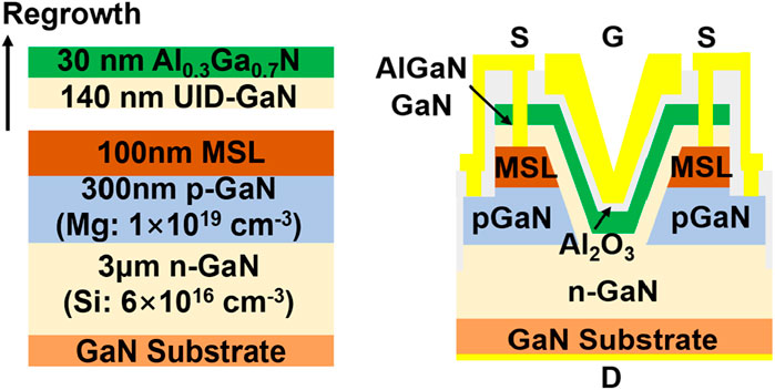
Figure 1. Schematic of trench CAVET fabricated on a GaN substrate.
The fabrication process of the trench CAVET is summarized in Figure 2. The structure was grown by MOCVD on a ∼400-μm GaN substrate with n + doping about 1 × 1018 cm−3, followed by a 3-μm n-GaN drift layer with a Si doping density of ∼6 × 1016 cm−3. A 300-nm p-GaN layer was grown as the CBL with Mg doping density of ∼1 × 1019 cm−3. On top of the p-GaN, another 100 nm of LT-GaN was grown at 1023 K to prevent Mg out-diffusion from p-GaN into the subsequent regrown layers. Trenches were etched to ∼500 nm deep using inductively coupled plasma reactive ion etching (ICP-RIE) to create the aperture region. After tetramethylammonium hydroxide (TMAH) wet etching to smooth the trench sidewalls (Kodama et al., 2008), UVO cleaning and HF treatment were performed immediately before the regrowth to reduce the Si concentration accumulating at the regrowth interface. The MOCVD regrowth contained 140 nm unintentionally doped (UID) GaN and 30 nm Al0.3Ga0.7N. Then, after device isolation by dry etching, the p-GaN CBL was activated by rapid thermal annealing (RTA). The Ti/Al/Ni/Au metal stack was deposited on AlGaN with lift-off, followed by RTA post-annealing at 1073 K to form an ohmic source contact. Ni/Au p-GaN contact was deposited on the exposed p-GaN surface. A 15 nm layer of Al2O3 was deposited by plasma atomic layer deposition (ALD) as a gate dielectric with post-deposition annealing (PDA) in N2. Ni/Au formed the gate contact covering the trench-shaped channel. A 170 nm SiO2 r was deposited as a passivation layer using plasma enhanced chemical vapor deposition (PECVD), followed by via opening. Ti/Au formed the gate and source pads and connected the p-GaN contact to the source. A Ti/Au drain electrode was placed on the backside.
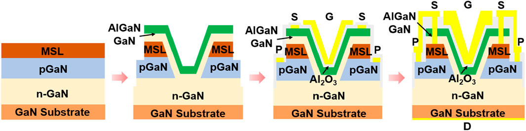
Figure 2. Schematic process flow of the GaN trench CAVET.
3 Experimental results
3.1 On the cryogenic characterization of GaN trench CAVET
CAVETs are unique among vertical GaN devices in that they employ a polarization-induced 2DEG channel, which enables a temperature-insensitive 2DEG channel without relying on impurity doping. This intrinsic conduction mechanism makes them highly attractive for cryogenic power electronics. Notably, in trench CAVETs, the AlGaN/GaN heterostructure that forms the 2DEG channel is ex situ regrown on a trench-shaped surface, with partial overlap on the p-GaN CBL. This geometry introduces challenges in the MOCVD regrowth process, particularly in achieving high-quality heterointerfaces and maintaining excellent 2DEG conductivity. Given that, we focused on characterizing the 2DEG transport properties and current conduction behavior of the trench CAVET across a wide temperature range. The fabricated wafer was measured using a cryogenic probe station equipped with liquid helium for temperature control, enabling electrical characterization down to approximately 10 K. We extracted the 2DEG charge density through capacitance–voltage (C–V) measurements at 1 MHz, as shown in Figure 3b. The C–V measurements were performed on a circular Schottky diode fabricated on the CAVET wafer (Figure 3a). The 2DEG charge density (ns) determined from C–V was 7.36 × 1012 cm−2 at 296 K and 6.83 × 1012 cm−2 at 10 K, indicating an almost negligible variation with temperature. The measured capacitance in the accumulation region is nearly flat, which shows the capacitance of the AlGaN barrier layer (CAlGaN). As the voltage bias becomes more negative, electrons in the 2DEG channel at the AlGaN/GaN heterojunction begin to gradually deplete under gate control, resulting in an increasing depletion width in the GaN layer. The total measured capacitance consists of the CAlGaN and the GaN depletion capacitance (Cdepletion) in series, as shown in Equation (1):
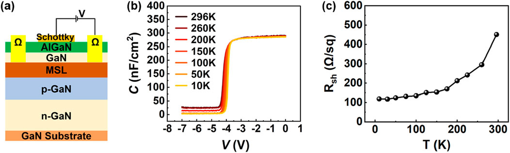
Figure 3. C–V characteristics and TLM of the regrown AlGaN/GaN heterostructure. (a) Circular Schottky diode for C–V measurements. (b) The C–V plot at different temperatures from 296 K to 10 K. (c) Temperature-dependent Rsh from TLM.
In the transition region where the 2DEG is almost depleted, the C–V curve slope becomes steeper as the temperature decreases from 296 K due to stronger electron confinement at the AlGaN/GaN interface at cryogenic temperatures (Liang et al., 2022; Nicollian and Brews, 2002; Miczek et al., 2008). When the gate bias falls below the threshold voltage, the 2DEG becomes fully depleted, and the C–V curve reaches a lower plateau. This region corresponds to the depletion capacitance of the UID-GaN channel and the MSL beneath the heterojunction. At cryogenic temperatures, the ionization rate of residual donors in GaN decreases, resulting in a wider depletion region and thus a lower capacitance.
The temperature dependence of the channel sheet resistance (Rsh) was extracted from the transfer length method (TLM), as presented in Figure 3c. Rsh decreased from 450.5 Ω/sq at 296 K to 118.9 Ω/sq at 10 K, which was primarily attributed to the improvement in 2DEG carrier mobility due to the reduction of scattering effects at lower temperatures (Zanato et al., 2004).
The transconductance (gm = ∂ID/∂VGS) extracted from ID–VGS at VDS = 0.1 V across different temperatures is shown in Figure 4. Measurements were conducted on a lateral trench channel structure with identical epitaxial layers to those of the CAVET, as illustrated in Figure 4a. The field-effect mobility (μFE) of the regrown AlGaN/GaN channel was calculated using (Equation 2) the following equation (Wei et al., 2015):
where LG/WG is the gate length-to-width ratio, and Cg is the capacitance between the gate and channel. The extracted mobility from the peak gm, as shown in Figure 4c, increased from 1886 cm2/(V∙s) at 296 K to 3577 cm2/(V∙s) at 10 K. In the relatively high-temperature range, polar optical (LO) phonon scattering is the dominant mobility-limiting mechanism for the 2DEG (Zanato et al., 2004; Kaasbjerg et al., 2013). As the temperature decreases from 296 K, the mobility limited by LO phonon scattering increases exponentially (Lisesivdin et al., 2010; Karmakar et al., 2023). Below approximately 100 K, the mobility gradually saturates and exhibits weak temperature dependence, consistent with prior reports (Zanato et al., 2004; Gökden, 2003). In this deep cryogenic regime, phonon-related scattering mechanisms are largely suppressed, and the remaining mobility limitation can be primarily attributed to interface roughness and dislocation scattering (Nedwell, 1999).
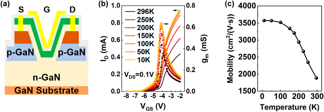
Figure 4. (a) Lateral trench structure on the GaN substrate, involving identical epitaxial layers to those of the CAVET. (b) Temperature-dependent ID–VGS with corresponding transconductance. (c) Extracted field-effect mobility as a function of temperature.
Figure 5a illustrates the temperature-dependent ID–VGS transfer characteristics of the trench CAVET in both logarithmic and linear scales. At lower temperatures, the off-state leakage current decreased due to the suppression of thermally generated carriers within the material (Kizilyalli and Aktas, 2015; Chen et al., 2024). Coupled with the increased on-state current at lower temperatures, the Ion/Ioff ratio improved significantly from 3 × 10⁹ at 296 K to 9 × 10¹⁰ at 10 K. The off-state leakage current decreased at lower temperatures, consistent with the reduced capacitance values observed in the lower plateau of the C–V curves in Figure 3b at cryogenic temperatures. The extracted subthreshold slope (SS) improved from 98.32 mV/dec at 296 K to 51.31 mV/dec at 10 K. Figure 5b shows the threshold voltage (VTH) defined at 1 μA/mm. No significant variation in VTH was observed across the temperature range, showing an average value of −7.45 V and a standard deviation of 0.069 V. The 2DEG at the AlGaN/GaN interface is primarily induced by polarization fields rather than doping, and the degenerate electron population in the 2DEG channel is nearly temperature-independent (Smorchkova et al., 1999). Because the ns strongly influences VTH (Huque et al., 2009), the observed VTH stability of CAVET is consistent with the fact that ns remained almost constant across temperatures.
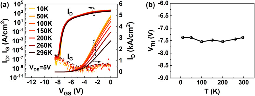
Figure 5. (a) Temperature-dependent ID–VGS transfer characteristics of the fabricated trench CAVET with as-grown MSL. (b) The extracted VTH across temperatures from 296 K to 10 K.
Figures 6a,b compare the ID–VDS output characteristics of the fabricated trench CAVET measured at 296 K and 10 K with the gate voltage swept from 0 V in steps of −1 V. At 296 K, the specific on-resistance (Ron,sp) was 1.02 mΩ cm2, and the maximum drain current density (ID,max) at VDS = 10 V and VGS = 0 V was 3.66 kA/cm2. At 10 K, Ron,sp decreased to 0.586 mΩ cm2, and ID,max increased to 5.82 kA/cm2. The normalized on-resistance at each temperature, defined as Ron,sp (T)/Ron,sp (296 K), is plotted in Figure 6c alongside data from a lateral trench HEMT (Figure 4a). As the temperature decreased from 296 K to 10 K, both devices exhibited a similar decreasing trend in Ron,sp, which continuously decreased as the temperature dropped from 296 K and gradually saturated below 100 K. At 10 K, the normalized Ron,sp of the lateral trench HEMT was 0.541, while that of the vertical CAVET was slightly higher at 0.576. The slightly less pronounced reduction in Ron,sp for the vertical CAVET, compared to the lateral counterpart, indicates additional contributions from drift resistance (Rdrift) and substrate resistance (Rsub). The Ron,sp in a CAVET primarily comprises the channel resistance (Rch), Rdrift, and Rsub (Chowdhury, 2019). In the fabricated trench CAVET with a 3-μm drift layer, Rch accounted for approximately 70% of Ron,sp at RT, and its temperature dependence was primarily governed by channel mobility, as the 2DEG charge density remained nearly constant. At cryogenic temperatures, the bulk electron mobility is primarily constrained by ionized impurity scattering, while the 2DEG channel experiences a more pronounced mobility enhancement (Lisesivdin et al., 2010; Shur et al., 1996).
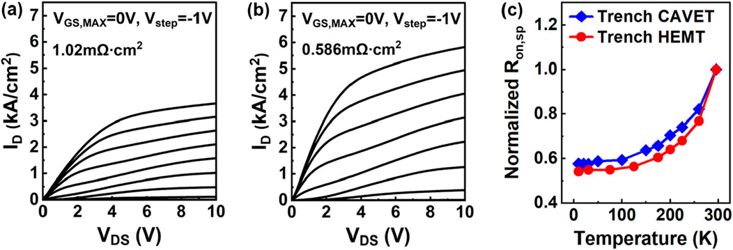
Figure 6. ID–VDS output characteristics of the fabricated trench CAVET at (a) 296 K and (b) 10 K. (c) Temperature-dependent normalized Ron,sp of the fabricated trench CAVET and trench HEMT.
3.2 On the high-temperature survivability of GaN trench CAVET
Thermal shock testing serves as an effective preliminary method to assess the resilience of devices under extreme temperature fluctuations and rapid thermal cycling. As an initial effort to explore the impact of elevated temperatures (≥773 K) on the fabricated GaN trench CAVETs, two samples were subjected to rapid thermal annealing (RTA) in a nitrogen ambient atmosphere for 1 minute at 773 K (500 °C) and 1073 K (800 °C), respectively.
One-minute 773 K thermal shock tests were performed three times on the trench CAVET. The post-annealing I–V characteristics, including both transfer and output curves, are presented in Figure 7 to explore the impact of repeated thermal shock tests on device transport properties. The devices retained typical FET behavior throughout the tests. The transfer characteristics in Figure 7a exhibit a positive VTH shift from −9.9 V before the thermal shock to −9.2 V after the first run, with no further obvious change observed after the second and third runs. The observed rightward shift in VTH after thermal shock tests may be attributed to annealing effects in the ALD-grown Al2O3 gate dielectric layer during thermal shock tests. Specifically, such annealing may reduce the trap state density either at the oxide/AlGaN interface or within the oxide layer, resulting in a positive shift in VTH (Nakazawa et al., 2019; Gupta et al., 2019). Additionally, gradual gate degradation was observed after the repeated thermal shock tests, as reflected by an increase in off-state gate leakage current from 10−5 A/cm2 to 10−3 A/cm2 after three cycles. The output curves in Figure 7b show that the Ron,sp increased to 1.58 mΩ cm2 after the first test and 1.60 mΩ cm2 after the third thermal test. The output current density at VGS = 0 V and VDS = 6 V decreased to 1892 A/cm2 after the first thermal test and 1819 A/cm2 after the third run.
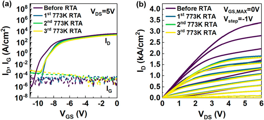
Figure 7. (a) ID–VGS transfer characteristics and (b) ID–VDS output characteristics trench CAVET after repeated 773 K thermal shock testing.
After exposure to 1073 K, the devices exhibited more severe performance degradation. As shown in Figure 8a, proper pinch-off behavior was no longer observed due to a substantial increase in gate leakage current. Extracted from the output characteristics in Figure 8b, the Ron,sp increased significantly to 24.2 mΩ cm2, and the output current density dropped to 170 A/cm2. Compared to the 773 K treatment, visible metal degradation and peel-off were observed at 1073 K, as shown in Figure 9, along with a distinct color change in the gate metal, indicating possible metal alloying contributing to the increased leakage.
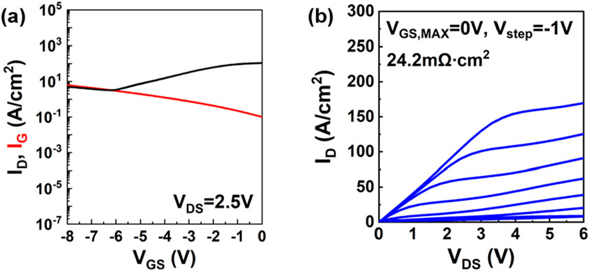
Figure 8. (a) ID–VDS and (b) ID–VGS of trench CAVET after 1073 K thermal shock testing.
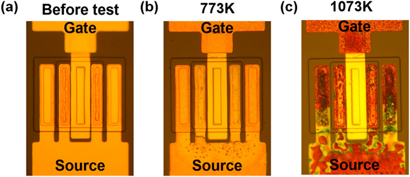
Figure 9. Optical images of trench CAVET (a) before testing, (b) after 773 K thermal shock, and (c) after 1073 K thermal shock.
These results represent the first demonstration of the thermal survivability of GaN trench CAVETs under high-temperature shocks and provide a foundation for future studies exploring their reliability under combined high-temperature and bias-stress conditions. The electrical characteristics of the GaN trench CAVETs from this work and our prior study (Wen et al., 2024c) are summarized in Table 1, including both in situ measurements (i.e., devices measured at the specified temperature) and ex-situ measurements (i.e., devices measured after undergoing 1-min thermal shock testing).
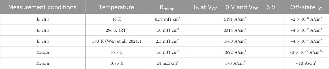
Table 1. A summary of the GaN trench CAVET performance in this work and in Wen et al. (2024c) at different temperatures, including both in situ measurements (i.e., devices measured at the specified temperature) and ex-situ measurements (i.e., devices measured after undergoing 1-min thermal shock testing). *Note that the minimum current measurement resolution of the source measurement unit (SMU) used for gate current measurement in ex-situ characterization is approximately 10−5 A/cm2. Currents below this threshold may not be accurately detected.
4 Conclusion
In summary, this study presents the first investigation of the device characterization of GaN trench CAVETs over a broad temperature range. For cryogenic characterization, the 2DEG charge density was 7.36 × 1012 cm−2 obtained from the regrown AlGaN/GaN channel with a slight 7% reduction from 296 K to 10 K. The VTH of CAVET exhibited excellent thermal stability. The field-effect mobility increased from 1886 cm2/(V∙s) at 296 K to 3577 cm2/(V∙s) at 10 K, contributing to improved device conductivity. Specifically, ID,max increased from 3.66 kA/cm2 to 5.82 kA/cm2, and Ron,sp decreased from 1.06 mΩ cm2 to 0.586 mΩ cm2. Additionally, we performed 1-min thermal shock testing to preliminarily evaluate the survivability of trench CAVETs under high-temperature conditions. The device maintained normal functionality after 773 K testing with approximately 50% current reduction. Exposure to 1073 K caused more significant degradation in both Ron,sp and gate control. These findings demonstrate the potential of GaN trench CAVETs for applications in extreme temperature environments.
Data availability statement
The raw data supporting the conclusions of this article will be made available by the authors, without undue reservation.
Author contributions
XW: Conceptualization, Data curation, Investigation, Methodology, Visualization, Writing – original draft, Writing – review and editing. KL: Conceptualization, Investigation, Methodology, Writing – original draft, Writing – review and editing. HK: Conceptualization, Investigation, Methodology, Resources, Validation, Visualization, Writing – original draft, Writing – review and editing. MN: Conceptualization, Investigation, Methodology, Writing – original draft, Writing – review and editing. CM: Conceptualization, Investigation, Methodology, Writing – original draft, Writing – review and editing. SC: Conceptualization, Funding acquisition, Investigation, Methodology, Project administration, Supervision, Writing – original draft, Writing – review and editing.
Funding
The author(s) declare that financial support was received for the research and/or publication of this article. This work is funded by KYOCERA Corporation, Japan. The funder was not involved in the study design, collection, analysis, interpretation of data, the writing of this article, or the decision to submit it for publication.
Acknowledgments
We are grateful for the support from KYOCERA Corporation, Japan. The devices were fabricated at the Stanford Nanofabrication Facility (SNF) and the Stanford Nano Shared Facilities (SNSF).
Conflict of interest
The authors declare that the research was conducted in the absence of any commercial or financial relationships that could be construed as a potential conflict of interest.
Generative AI statement
The author(s) declare that no Generative AI was used in the creation of this manuscript.
Publisher’s note
All claims expressed in this article are solely those of the authors and do not necessarily represent those of their affiliated organizations, or those of the publisher, the editors and the reviewers. Any product that may be evaluated in this article, or claim that may be made by its manufacturer, is not guaranteed or endorsed by the publisher.
References
Ahmad, N. (1987). Carrier freeze-out effects in semiconductor devices. J. Appl. Phys. 61 (5), 1905–1909. doi:10.1063/1.338037
Chen, S., Cai, C., Wang, T., Guo, Q., and Sheng, K. (2013). “Cryogenic and high temperature performance of 4H-SiC power MOSFETs,” in 2013 twenty-eighth annual IEEE applied power electronics conference and exposition (APEC), 207–210.
Chen, Y.-H., Chu, F. C., Uma, M., Aslam, M., Lee, Y. J., Li, Y., et al. (2024). Threshold voltage stability in AlGaN/GaN MIS-HEMT structure under cryogenic environment. IEEE Trans. Electron Devices 71, 6566–6572. doi:10.1109/ted.2024.3457581
Chowdhury, S. (2019). “GaN-on-GaN power device design and fabrication,” in Wide bandgap semiconductor power devices (Elsevier), 209–248.
Chowdhury, S., and Mishra, U. K. (2013). Lateral and vertical transistors using the AlGaN/GaN heterostructure. IEEE Trans. Electron Devices 60 (10), 3060–3066. doi:10.1109/ted.2013.2277893
Chowdhury, S., Swenson, B. L., and Mishra, U. K. (2008). Enhancement and depletion mode AlGaN/GaN CAVET with Mg-Ion-Implanted GaN as current blocking layer. IEEE Electron Device Lett. 29 (6), 543–545. doi:10.1109/LED.2008.922982
Chowdhury, S., Wong, M. H., Swenson, B. L., and Mishra, U. K. (2012). CAVET on bulk GaN substrates achieved with MBE-regrown AlGaN/GaN layers to suppress dispersion. IEEE Electron Device Lett. 33 (1), 41–43. doi:10.1109/led.2011.2173456
Döring, P. (2024). Towards vertical GaN-power ICs: Co-integration of lateral HEMTs and vertical power CAVETs. IEEE, 382–385.
Fu, K., Fu, H., Deng, X., Su, P. Y., Liu, H., Hatch, K., et al. (2021). The impact of interfacial Si contamination on GaN-on-GaN regrowth for high power vertical devices. Appl. Phys. Lett. 118 (22). doi:10.1063/5.0049473
Fu, K., Fu, H., Huang, X., Chen, H., Yang, T. H., Montes, J., et al. (2019). Demonstration of 1.27 kV etch-then-regrow GaN p - n junctions with low leakage for GaN power electronics. IEEE Electron Device Lett. 40 (11), 1728–1731. doi:10.1109/LED.2019.2941830
Gökden, S. (2003). Mobility of two-dimensional electrons in an AlGaN/GaN modulation-doped heterostructure. Phys. status solidi (a) 200 (2), 369–377. doi:10.1002/pssa.200306701
Gui, H., Chen, R., Niu, J., Zhang, Z., Tolbert, L. M., Wang, F. F., et al. (2020). Review of power electronics components at cryogenic temperatures. IEEE Trans. Power Electron 35 (5), 5144–5156. doi:10.1109/tpel.2019.2944781
Gupta, S. D., Soni, A., Joshi, V., Kumar, J., Sengupta, R., Khand, H., et al. (2019). Positive threshold voltage shift in AlGaN/GaN HEMTs and E-mode operation by AlxTi1-x O based gate stack engineering. IEEE Trans. Electron Devices 66 (6), 2544–2550. doi:10.1109/ted.2019.2908960
Hassan, A., Savaria, Y., and Sawan, M. (2018). GaN integration technology, an ideal candidate for high-temperature applications: a review. IEEE Access 6, 78790–78802. doi:10.1109/access.2018.2885285
Huque, M., Eliza, S., Rahman, T., Huq, H., and Islam, S. (2009). Temperature dependent analytical model for current–voltage characteristics of AlGaN/GaN power HEMT. Solid-State Electron. 53 (3), 341–348. doi:10.1016/j.sse.2009.01.004
Jeong, S., Lee, K., Chun, J., Soman, R., and Chowdhury, S. (2023). Scaling study on high-current density low-dispersion GaN vertical FinFETs. IEEE Electron Device Lett. 44 (5), 841–844. doi:10.1109/led.2023.3259002
Ji, D. (2017). “Demonstrating> 1.4 kV OG-FET performance with a novel double field-plated geometry and the successful scaling of large-area devices,” in 2017 IEEE international electron devices meeting (IEDM) (IEEE), 9.4. 1–9.4. 4.
Ji, D., Agarwal, A., Li, H., Li, W., Keller, S., and Chowdhury, S. (2018a). 880 V/2.7 mΩ⋅cm2 MIS Gate Trench CAVET on Bulk GaN Substrates. IEEE Electron Device Lett. 39 (6), 863–865. doi:10.1109/led.2018.2828844
Ji, D., Agarwal, A., Li, W., Keller, S., and Chowdhury, S. (2018b). Demonstration of GaN current aperture vertical electron transistors with aperture region formed by ion implantation. IEEE Trans. Electron Devices 65 (2), 483–487. doi:10.1109/ted.2017.2786141
Ji, D., Yue, Y., Gao, J., and Chowdhury, S. (2016). Dynamic modeling and power loss analysis of high-frequency power switches based on GaN CAVET. IEEE Trans. Electron Devices 63 (10), 4011–4017. doi:10.1109/ted.2016.2601559
Kaasbjerg, K., Thygesen, K. S., and Jauho, A.-P. (2013). Acoustic phonon limited mobility in two-dimensional semiconductors: deformation potential and piezoelectric scattering in monolayer MoS 2 from first principles. Phys. Rev. B—Condensed Matter Mater. Phys. 87 (23), 235312. doi:10.1103/physrevb.87.235312
Karmakar, C., Kaneriya, R. K., Malasi, M., Rathod, S., Kumar, D., Chakravarty, S., et al. (2023). Enhanced quantum oscillations and scattering effect in quaternary InAlGaN/GaN two-dimensional electron gas. Appl. Phys. Lett. 122 (20). doi:10.1063/5.0142605
Kizilyalli, I. C., and Aktas, O. (2015). Characterization of vertical GaN p–n diodes and junction field-effect transistors on bulk GaN down to cryogenic temperatures. Semicond. Sci. Technol. 30 (12), 124001. doi:10.1088/0268-1242/30/12/124001
Kodama, M., Sugimoto, M., Hayashi, E., Soejima, N., Ishiguro, O., Kanechika, M., et al. (2008). GaN-based trench gate metal oxide semiconductor field-effect transistor fabricated with novel wet etching. Appl. Phys. Express 1, 021104. doi:10.1143/apex.1.021104
Li, W., Xing, H. G., Nomoto, K., Lee, K., Islam, S., Hu, Z., et al. (2018). Development of GaN vertical trench-MOSFET with MBE regrown channel. IEEE Trans. Electron Devices 65 (6), 2558–2564. doi:10.1109/ted.2018.2829125
Liang, L., Yongfeng, Y., Heqiu, Z., Huanhuan, C., He, X., Tao, C., et al. (2022). The interface trap analysis of AlGaN/GaN high electron mobility transistors with temperature based on conductance method. J. Phys.: Conf. Ser. 2248 (1), 012016. doi:10.1088/1742-6596/2248/1/012016
Lisesivdin, S. B., Yildiz, A., Balkan, N., Kasap, M., Ozcelik, S., and Ozbay, E. (2010). Scattering analysis of two-dimensional electrons in AlGaN/GaN with bulk related parameters extracted by simple parallel conduction extraction method. J. Appl. Phys. 108 (1), 013712. doi:10.1063/1.3456008
Liu, J. (2020). “1.2 kV vertical GaN fin JFETs with robust avalanche and fast switching capabilities,” in Presented at the 2020 IEEE international electron devices meeting (IEDM).
Miczek, M., Mizue, C., Hashizume, T., and Adamowicz, B. (2008). Effects of interface states and temperature on the CV behavior of metal/insulator/AlGaN/GaN heterostructure capacitors. J. Appl. Phys. 103 (10). doi:10.1063/1.2924334
Nakazawa, S., Shih, H. A., Tsurumi, N., Anda, Y., Hatsuda, T., Ueda, T., et al. (2019). Effects of post-deposition annealing in O2 on threshold voltage of Al2O3/AlGaN/GaN MOS heterojunction field-effect transistors. Jpn. J. Appl. Phys. 58 (3), 030902. doi:10.7567/1347-4065/aafd17
Nedwell, D. B. (1999). Effect of low temperature on microbial growth: lowered affinity for substrates limits growth at low temperature. FEMS Microbiol. Ecol. 30 (2), 101–111. doi:10.1111/j.1574-6941.1999.tb00639.x
Nela, L., Perera, N., Erine, C., and Matioli, E. (2021). Performance of GaN power devices for cryogenic applications down to 4.2 K. IEEE Trans. Power Electron. 36 (7), 7412–7416. doi:10.1109/tpel.2020.3047466
Nicollian, E. H., and Brews, J. R. (2002). MOS (metal oxide semiconductor) physics and technology. John Wiley and Sons.
Noshin, M., Soman, R., Xu, X., and Chowdhury, S. (2022). A systematic study of the regrown interface impurities in unintentionally doped Ga-polar c-plane GaN and methods to reduce the same. Semicond. Sci. Technol. 37 (7), 075018. doi:10.1088/1361-6641/ac71bf
Oka, T., Ina, T., Ueno, Y., and Nishii, J. (2015). 1.8 mΩ· cm2 vertical GaN-based trench metal–oxide–semiconductor field-effect transistors on a free-standing GaN substrate for 1.2-kV-class operation. Appl. Phys. Express 8 (5), 054101. doi:10.7567/apex.8.054101
Rajashekara, K., and Akin, B. (2013). “A review of cryogenic power electronics - status and applications,” in 2013 international electric machines and drives conference, 899–904. doi:10.1109/IEMDC.2013.6556204
Shibata, D. (2016). “1.7 kV/1.0 mΩcm 2 normally-off vertical GaN transistor on GaN substrate with regrown p-GaN/AlGaN/GaN semipolar gate structure,” in 2016 IEEE international electron devices meeting (IEDM) (IEEE), 10.1. 1–10.1. 4.
Shur, M., Gelmont, B., and Asif Khan, M. (1996). Electron mobility in two-dimensional electron gas in AIGaN/GaN heterostructures and in bulk GaN. J. Electron. Mater. 25, 777–785. doi:10.1007/bf02666636
Smorchkova, I., Elsass, C. R., Ibbetson, J. P., Vetury, R., Heying, B., Fini, P., et al. (1999). Polarization-induced charge and electron mobility in AlGaN/GaN heterostructures grown by plasma-assisted molecular-beam epitaxy. J. Appl. Phys. 86 (8), 4520–4526. doi:10.1063/1.371396
Wei, J., Liu, S., Tang, X., Lu, Y., Liu, C., et al. (2015). Low on-resistance normally-off GaN double-channel metal–oxide–semiconductor high-electron-mobility transistor. IEEE Electron Device Lett. 36 (12), 1287–1290. doi:10.1109/LED.2015.2489228
Wen, X. (2024). “Wrap-around gate delivering 600V/1.0 mΩ⋅cm2, normally-off, dispersion-free CAVETs with record-high gate swing,” in 2024 IEEE international electron devices meeting (IEDM), 1–4. doi:10.1109/IEDM50854.2024.10873443
Wen, X., Kasai, H., Lee, K., Noshin, M., Chun, J., and Chowdhury, S. (2024a). “First experimental demonstration of monolithic bidirectional switch using GaN current aperture vertical electron transistor (CAVET),” in Device research conference (DRC) (USA).
Wen, X., Kasai, H., Noshin, M., Meng, C., and Chowdhury, S. (2024b). Monolithic bidirectional GaN-on-GaN vertical transistor technologies: exploring bidirectional CAVET for next-generation switching applications with symmetrical power control. IEEE Electron Devices Mag. 2 (4), 36–41. doi:10.1109/MED.2024.3451353
Wen, X., Lee, K. J., Nakazato, Y., Chun, J., and Chowdhury, S. (2023). High current density trench CAVET on bulk GaN substrates with low-temperature GaN suppressing Mg diffusion. Crystals 13 (4), 709. doi:10.3390/cryst13040709
Wen, X., Shankar, B., Lee, K., Kasai, H., Noshin, M., Chun, J., et al. (2024c). 10 MHz-switching on GaN trench CAVET up to 300° C operation enabled by high channel mobility. IEEE Electron Device Lett. 45, 653–656. doi:10.1109/led.2024.3360917
Xing, H., Green, D. S., Yu, H., Mates, T., Kozodoy, P., Keller, S., et al. (2003). Memory effect and redistribution of Mg into sequentially regrown GaN layer by metalorganic chemical vapor deposition. Jpn. J. Appl. Phys. 42 (1), 50–53. doi:10.1143/jjap.42.50
Yuan, M. (2022). “High temperature robustness of enhancement-mode p-GaN-gated AlGaN/GaN HEMT technology,” in 2022 IEEE 9th workshop on wide bandgap power devices and applications (WiPDA) (IEEE), 40–44.
Zanato, D., Gokden, S., Balkan, N., Ridley, B., and Schaff, W. J. (2004). The effect of interface-roughness and dislocation scattering on low temperature mobility of 2D electron gas in GaN/AlGaN. Semicond. Sci. Technol. 19 (3), 427–432. doi:10.1088/0268-1242/19/3/024
Keywords: gallium nitride, current aperture vertical electron transistor, vertical transistor, cryogenic electronics, high-temperature electronics, extreme temperature applications
Citation: Wen X, Lee K, Kasai H, Noshin M, Meng C and Chowdhury S (2025) Exploring the performance of GaN trench CAVETs from cryogenic to elevated temperatures. Front. Electron. 6:1613402. doi: 10.3389/felec.2025.1613402
Received: 17 April 2025; Accepted: 17 July 2025;
Published: 12 August 2025.
Edited by:
Wenping Zhang, Tianjin University, ChinaCopyright © 2025 Wen, Lee, Kasai, Noshin, Meng and Chowdhury. This is an open-access article distributed under the terms of the Creative Commons Attribution License (CC BY). The use, distribution or reproduction in other forums is permitted, provided the original author(s) and the copyright owner(s) are credited and that the original publication in this journal is cited, in accordance with accepted academic practice. No use, distribution or reproduction is permitted which does not comply with these terms.
*Correspondence: S. Chowdhury, c3JhYmFudGlAc3RhbmZvcmQuZWR1