 Zhiying Dan1
 Ronak Sarmasti Emami1Giovanna Feraco1Melina Vavali1,2Dominic Gerlach1Martin F Sarott1,3Yindi Zhu1
 Petra Rudolf1
 Antonija Grubišić-Čabo1*
- 1Zernike Institute for Advanced Materials, University of Groningen, Groningen, Netherlands
- 2Sorbonne Université, CNRS, MONARIS, UMR 8233, Paris, France
- 3Groningen Cognitive Systems and Materials Center (CogniGron), University of Groningen, Groningen, Netherlands
Two-dimensional (2D) transition metal dichalcogenides have emerged as a promising platform for next-generation optoelectronic and spintronic devices. Mechanical exfoliation using adhesive tape remains the dominant method for preparing 2D materials of highest quality, including transition metal dichalcogenides, but always results in small-sized flakes. This limitation poses a significant challenge for investigations and applications where large scale flakes are needed. To overcome these constraints, we explored the preparation of 2D
1 Introduction
In recent years two-dimensional (2D) materials have gained significant attention due to their unique electronic and optical properties, such as the transition from an indirect to a direct band gap when going from bulk to a single layer of
The challenges are further exacerbated when handling air- or moisture-sensitive 2D materials, such as black phosphorus and
Recently, the metal-assisted mechanical exfoliation technique has emerged as a feasible solution for large-area 2D material production (Wu et al., 2024a; Petrini et al., 2024; Grubišić-Čabo et al., 2023; Liu et al., 2020). By exploiting the stronger adhesion between the metals and the outermost layer of bulk layered crystals, this technique can produce monolayers on a millimeter–or even centimeter–scale by pressing a tape containing a bulk crystal on clean, smooth metal substrates, such as gold (Liu et al., 2020). The resulting large lateral size is crucial for device fabrication and characterization, facilitating standard photolithography, scalable manufacturing, and high-quality 2D heterostructure integration, while also meeting the dimensional requirements of techniques like X-ray photoelectron spectroscopy (XPS) for reliable material analysis. However, this method is typically performed under ambient conditions, making it unsuitable for air-sensitive materials. Moreover, this method is incompatible with surface techniques that require in situ surface cleaning.
Here, we employed an ultra-high vacuum (UHV) exfoliation method (Grubišić-Čabo et al., 2023) to prepare large-area monolayers of TMDC films. While having the same advantages as ME over bottom-up synthesis techniques, our method also performs better for certain applications over liquid-phase exfoliation. Liquid phase exfoliation produces exfoliated monolayers that typically have lower crystalline quality, higher defect density, and smaller lateral dimensions, albeit in a high quantity, and our method provides better control of the sheet size and thickness, provided the substrate is suitable for this approach (Paton et al., 2014). The comparison of various exfoliation methods can be found in the Supplementary Table S2. Using the aforementioned UHV exfoliation approach we successfully produced near-millimeter-scale monolayers of
2 Materials and methods
2.1 Materials
Ag (111)/mica and Au (111)/mica (Georg-Albert-PVD) substrates were cut to the appropriate size and fixed to a flag style sample plate by welded tantalum strips. The Au and Ag substrates were cleaned using repeated cycles of Ar+ sputtering (45 min at
2.2 Characterization techniques
2.2.1 Low-energy electron diffraction
LEED measurements (SPECS ErLEED 1000A) with a 1 mm spot size were performed at room temperature under a pressure of
2.2.2 Optical microscopy
Monolayers of exfoliated materials were identified using optical contrast technique. Optical images were acquired with an Olympus microscope and processed using ImageJ software to analyze regions corresponding to monolayer contrast. The images were split into red, green and blue (RGB) channels, with the red channel selected for analysis due to its excellent contrast. ImageJ threshold routines were applied to identify flakes and calculate monolayer areas as well as lateral sizes, represented by the maximum Feret diameter. Statistical analysis of the size distributions was performed by fitting the data to a log-normal distribution.
2.2.3 Atomic force microscopy
AFM was conducted under ambient conditions with Dimension FastScan Bruker and Cypher S AFM (Asylum Research) microscopes using the AC160-TSA tip. The measurements were performed in tapping mode. The AFM was calibrated using a standard calibration sample prior to the experiments. AFM data analysis was carried out using the Gwyddion software package.
The Kelvin probe force microscopy (KPFM) measurements were performed on an Asylum Research Cypher ES atomic force microscope using Co/Cr-coated Sb-doped Si tips from Bruker (MESP-RC-V2, k = 5 N/m,
2.2.4 Scanning electron microscopy
Scanning electron microscopy (SEM) characterization was performed using a FEI NovaNano NanoSEM 650 instrument operated at an acceleration voltage of 10 kV in secondary electrons mode. The sample was supported to a metal stub using conductive double-sided carbon tape to hold the sample securely.
2.2.5 X-ray photoelectron spectroscopy
XPS measurements of the TMDC/metal samples were performed using an SSX-100 (Surface Science Instruments) spectrometer equipped with a monochromatic Al K
3 Results and discussion
3.1 Exfoliation of monolayers in UHV
Samples were prepared using the kinetic in situ single-layer synthesis (KISS) method, as illustrated in Figure 1 for the case of
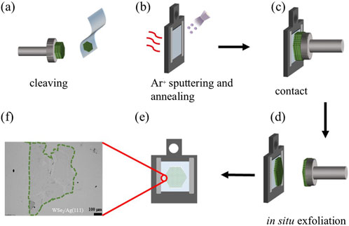
Figure 1. A schematic of the kinetic in situ single layer synthesis (KISS) exfoliation process: (a) preparation of an ultra-flat, clean
3.2 Surface morphology and structure
3.2.1 Angular alignment with the substrate
Following exfoliation procedure, in situ characterization was conducted using the LEED system mounted on the same UHV chamber. As shown in Figure 2, LEED patterns were obtained for four individual flakes exfoliated onto Au (111), Figure 2a, and Ag (111) substrates, Figure 2b. All pattern exhibited distinct nested hexagonal diffraction patterns, consistent with the hexagonal crystalline lattices of
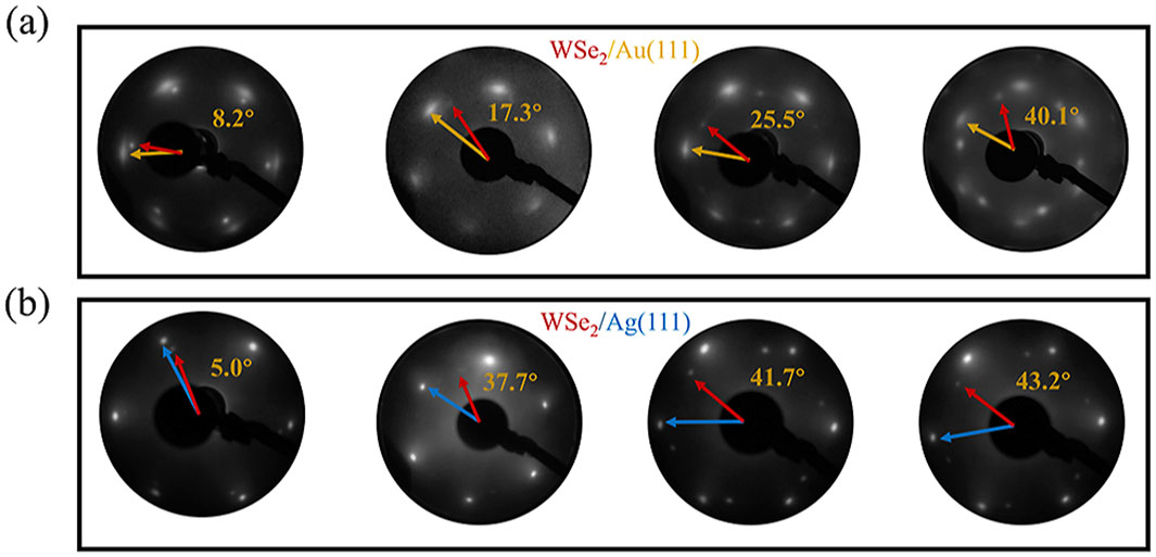
Figure 2. Low-energy electron diffraction (LEED) analysis of the rotational alignment between the exfoliated 2D material and the substrate: (a) LEED images of
Epitaxially grown 2D materials typically exhibit preferred stacking orientation relative to the substrate they are grown on (Choudhury et al., 2020). However, KISS exfoliation does not favor a specific stacking orientation alignment between the exfoliated 2D materials and its substrates, as seen from the LEED patterns. Table 1 summarizes the twist angles derived from Figure 2 and Supplementary Figure S1, showing significant angular variations between the TMDC flakes and the substrates, with angles randomly distributed between 0° and 60°. Furthermore, lattice matching between the metal substrate and the TMDC seems to have no effect on the exfoliation process. In other words, we can exclude that grains in the parent crystal of Au (Ag) with a specific orientation with respect to the TMDC substrate attach more easily (Haider et al., 2024).
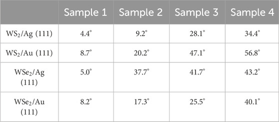
Table 1. Summary of twist angles between TMDCs and substrates based on LEED images of
3.2.2 Role of chalcogen atom
The presence of different chalcogen atoms influences various intrinsic properties of TMDCs (Huang et al., 2020), but their influence on KISS exfoliation trends remains unclear. Figure 3 presents the exfoliation results of WS2 and WSe2 on Ag (111) substrates, as observed by optical microscopy. Despite using the same type of substrate and proceeding with the exfoliation in an identical manner, differences in exfoliation yield between the two materials are clearly evident. For WSe2/Ag (111) sample, shown in Figure 3a, large and crack-free monolayer flakes were consistently produced, up to a maximum lateral size of 750
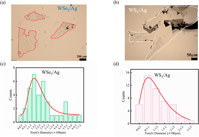
Figure 3. Optical microscopy characterization of exfoliated flake size distribution: (a) and (b) are representative optical images of
To quantitatively evaluate the yield of monolayer flakes, we measured and analyzed the size distribution of flakes from four different samples. Given the predominantly irregular morphology of the exfoliated flakes, the Feret diameter was used to determine their lateral dimensions (Petrini et al., 2024; Kröner and Hirsch, 2020). Using ImageJ software, the Feret diameters were extracted by manually applying an appropriate threshold, which meant setting the contrast range manually, where pixels above the threshold are considered as TMDC, while those below are attributed to the substrate (Schneider et al., 2012; Puebla et al., 2022). As shown in Figure 3c, the statistical size distribution for the four
The larger dimensions of
3.2.3 Surface morphology
To investigate the flake thickness, optical microscopy, Figure 4a, and AFM, Figure 4b, were used. The distinct color distribution observed in the optical images clearly indicates regions of varying thickness (Puebla et al., 2022). The step profile analysis showed that the monolayer thickness is approximately 0.82 nm, which is slightly larger than previously reported values for monolayer
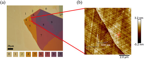
Figure 4. Thickness characterization based on color variations observed in the optical microscopy image: (a) optical image of the
In the AFM topography, a distinct regular pattern can also be observed, marked with red arrows in Figure 4b, which appears to originate from the underlying substrate. The angle between the lines in the pattern is exactly 60
3.3 Chemical composition and interfacial properties
We performed XPS measurements to better understand the interaction between TMDCs and metal surfaces.
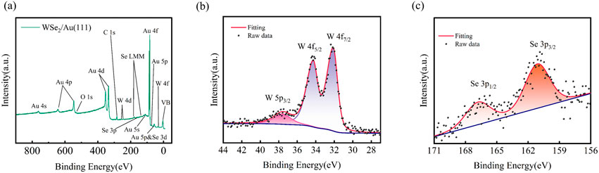
Figure 5. X-ray photoelectron spectroscopy (XPS) characterization of
Figures 5b,c show detailed spectra for W 4f and Se 3p. The asymmetry observed in the W 4f peak is attributed to shake-up events, promoting conduction electrons from below to above the Fermi level. The Se 3
Since KISS exfoliation involves the mechanical contact of a bulk crystal with another solid surface, it is essential to assess whether the process induces any damage to the substrate. To evaluate the impact of exfoliation on the substrate, we measured the (111) Bragg reflection of a single-crystal silver substrate in a near-backscattering geometry (see Section 4 in SI), which is sensitive to deformation of the substrate lattice. The measurement was performed with a focused beam aligned to a
4 Conclusion
The KISS exfoliation method has proven to be a reliable method for producing high-quality large-area monolayers of WS2 and WSe2, on metallic substrates in ultra-high vacuum. Notably, exfoliation of
Data availability statement
The datasets presented in this study can be found in online repositories. The names of the repository/repositories and accession number(s) can be found below: Zenodo: https://doi.org/10.5281/zenodo.14537302.
Author contributions
ZD: Conceptualization, Formal Analysis, Investigation, Visualization, Writing – original draft, Writing – review and editing. RSE: Formal Analysis, Investigation, Writing – review and editing. GF: Investigation, Writing – review and editing. MV: Investigation, Writing – review and editing. DG: Investigation, Writing – review and editing. MFS: Writing – original draft, Writing – review and editing, Investigation, Data curation, Formal analysis. YZ: Writing – original draft, Writing – review and editing, Investigation, Data curation. PR: Resources, Supervision, Writing – review and editing. AG-C: Conceptualization, Funding acquisition, Investigation, Project administration, Supervision, Writing – original draft, Writing – review and editing.
Funding
The author(s) declare that financial support was received for the research and/or publication of this article. This work was supported by the Zernike Institute for Advanced Materials. AG-C and PR acknowledge the research program “Materials for the Quantum Age” (QuMat) for financial support. This program (registration number 024.005.006) is part of the Gravitation program financed by the Dutch Ministry of Education, Culture and Science (OCW). ZD acknowledges the fellowship from the Chinese Scholarship Council (No. 202206750016).
Acknowledgments
AG-C acknowledges financial support of the Zernike Institute for Advanced Materials. AG-C and PR acknowledge the research program “Materials for the Quantum Age” (QuMat) for financial support. This program (registration number 024.005.006) is part of the Gravitation program financed by the Dutch Ministry of Education, Culture and Science (OCW). ZD acknowledges the fellowship from the Chinese Scholarship Council (No.202206750016). The authors would like to thank Diamond Light Source for beamtime (proposal SI35796) and the staff of beamline I09, Deepnarayan Biswas and Tien-Lin Lee, for their assistance with experiments and data collection.
Conflict of interest
The authors declare that the research was conducted in the absence of any commercial or financial relationships that could be construed as a potential conflict of interest.
Generative AI statement
The author(s) declare that no Gen AI was used in the creation of this manuscript.
Publisher’s note
All claims expressed in this article are solely those of the authors and do not necessarily represent those of their affiliated organizations, or those of the publisher, the editors and the reviewers. Any product that may be evaluated in this article, or claim that may be made by its manufacturer, is not guaranteed or endorsed by the publisher.
Supplementary material
The Supplementary Material for this article can be found online at: https://www.frontiersin.org/articles/10.3389/fnano.2025.1553976/full#supplementary-material
References
Ahangar, R. M., and Farmanzadeh, D. (2023). Effects of hexagonal boron nitride encapsulation on the electronic properties of Cu, Li, and O-doped black phosphorus monolayer. Phys. B Condens. Matter 660, 414880. doi:10.1016/j.physb.2023.414880
Beyer, H., Rohde, G., Grubišić Čabo, A., Stange, A., Jacobsen, T., Bignardi, L., et al. (2019). 80% Valley Polarization of free carriers in singly oriented single-layer WS2 on Au (111). Phys. Rev. Lett. 123, 236802. doi:10.1103/physrevlett.123.236802
Biesinger, M. C. (2022). Accessing the robustness of adventitious carbon for charge referencing (correction) purposes in XPS analysis: insights from a multi-user facility data review. Appl. Surf. Sci. 597, 153681. doi:10.1016/j.apsusc.2022.153681
Bignardi, L., Lizzit, D., Bana, H., Travaglia, E., Lacovig, P., Sanders, C. E., et al. (2019). Growth and structure of singly oriented single-layer tungsten disulfide on Au (111). Phys. Rev. Mater. 3, 014003. doi:10.1103/physrevmaterials.3.014003
Buapan, K., Somphonsane, R., Chiawchan, T., and Ramamoorthy, H. (2021). Versatile, low-cost, and portable 2D material transfer setup with a facile and highly efficient DIY inert-atmosphere glove compartment option. ACS Omega 6, 17952–17964. doi:10.1021/acsomega.1c01582
Carré, E., Sponza, L., Lusson, A., Stenger, I., Roux, S., Fossard, F., et al. (2024). Luminescence of black phosphorus films: exfoliation-induced defects and confined excitations. Phys. Rev. B 109, 035424. doi:10.1103/physrevb.109.035424
Castle, J., Chapman-Kpodo, H., Proctor, A., and Salvi, A. M. (2000). Curve-fitting in XPS using extrinsic and intrinsic background structure. J. Electron Spectrosc. Relat. Phenom. 106, 65–80. doi:10.1016/s0368-2048(99)00089-4
Choudhury, T. H., Zhang, X., Al Balushi, Z. Y., Chubarov, M., and Redwing, J. M. (2020). Epitaxial growth of two-dimensional layered transition metal dichalcogenides. Annu. Rev. Mater. Res. 50, 155–177. doi:10.1146/annurev-matsci-090519-113456
Chuang, H.-J., Phillips, M., McCreary, K. M., Wickramaratne, D., Rosenberger, M. R., Oleshko, V. P., et al. (2022). Emergent moiré phonons due to zone folding in WSe2–WS2 Van Der Waals Heterostructures. ACS Nano 16, 16260–16270. doi:10.1021/acsnano.2c05204
Dendzik, M., Bruix, A., Michiardi, M., Ngankeu, A. S., Bianchi, M., Miwa, J. A., et al. (2017). Substrate-induced semiconductor-to-metal transition in monolayer WS2. Phys. Rev. B 96, 235440. doi:10.1103/physrevb.96.235440
Ellis, J. K., Lucero, M. J., and Scuseria, G. E. (2011). The indirect to direct band gap transition in multilayered MoS2 as predicted by screened hybrid density functional theory. Appl. Phys. Lett. 99. doi:10.1063/1.3672219
Fang, H., Chuang, S., Chang, T. C., Takei, K., Takahashi, T., and Javey, A. (2012). High-performance single layered WSe2 p-FETs with chemically doped contacts. Nano Lett. 12, 3788–3792. doi:10.1021/nl301702r
Feraco, G., De Luca, O., Przybysz, P., Jafari, H., Zheliuk, O., Wang, Y., et al. (2024). Nano-ARPES investigation of structural relaxation in small angle twisted bilayer tungsten disulfide. Phys. Rev. Mater. 8, 124004. doi:10.1103/physrevmaterials.8.124004
Freedy, K. M., and McDonnell, S. J. (2020). Contacts for molybdenum disulfide: interface chemistry and thermal stability. Materials 13, 693. doi:10.3390/ma13030693
Gammelgaard, L., Whelan, P. R., Booth, T. J., and Bøggild, P. (2021). Long-term stability and tree-ring oxidation of WSe2 using phase-contrast AFM. Nanoscale 13, 19238–19246. doi:10.1039/d1nr05413a
Georgiou, T., Jalil, R., Belle, B. D., Britnell, L., Gorbachev, R. V., Morozov, S. V., et al. (2013). Vertical field-effect transistor based on graphene–WS2 heterostructures for flexible and transparent electronics. Nat. Nanotechnol. 8, 100–103. doi:10.1038/nnano.2012.224
Grubišić-Čabo, A., Michiardi, M., Sanders, C. E., Bianchi, M., Curcio, D., Phuyal, D., et al. (2023). In situ exfoliation method of large-area 2D materials. Adv. Sci. 10, 2301243. doi:10.1002/advs.202301243
Haider, G., Gastaldo, M., Karim, B., Plsek, J., Varade, V., Volochanskyi, O., et al. (2024). Highly efficient bulk-crystal-sized exfoliation of 2D materials under ultrahigh vacuum. ACS Appl. Electron. Mater. 6, 2301–2308. doi:10.1021/acsaelm.3c01824
Huang, Y., Pan, Y.-H., Yang, R., Bao, L.-H., Meng, L., Luo, H.-L., et al. (2020). Universal mechanical exfoliation of large-area 2D crystals. Nat. Commun. 11, 2453. doi:10.1038/s41467-020-16266-w
Islam, M. A., Serles, P., Kumral, B., Demingos, P. G., Qureshi, T., Meiyazhagan, A., et al. (2022). Exfoliation mechanisms of 2D materials and their applications. Appl. Phys. Rev. 9. doi:10.1063/5.0090717
Kezilebieke, S., Huda, M. N., Dreher, P., Manninen, I., Zhou, Y., Sainio, J., et al. (2020). Electronic and magnetic characterization of epitaxial VSe2 monolayers on superconducting NbSe2. Commun. Phys. 3, 116. doi:10.1038/s42005-020-0377-4
Kim, H.-U., Kanade, V., Kim, M., Kim, K. S., An, B.-S., Seok, H., et al. (2020). Wafer-scale and low-temperature growth of 1T-WS2 film for efficient and stable hydrogen evolution reaction. Small 16, 1905000. doi:10.1002/smll.201905000
Kröner, A., and Hirsch, T. (2020). Current trends in the optical characterization of two-dimensional carbon nanomaterials. Front. Chem. 7, 927. doi:10.3389/fchem.2019.00927
Li, L., Li, S., Wang, W., Zhang, J., Sun, Y., Deng, Q., et al. (2024). Adaptative machine vision with microsecond-level accurate perception beyond human retina. Nat. Commun. 15, 6261. doi:10.1038/s41467-024-50488-6
Liu, F., Wu, W., Bai, Y., Chae, S. H., Li, Q., Wang, J., et al. (2020). Disassembling 2D van der Waals crystals into macroscopic monolayers and reassembling into artificial lattices. Science 367, 903–906. doi:10.1126/science.aba1416
Man, M. K., Deckoff-Jones, S., Winchester, A., Shi, G., Gupta, G., Mohite, A. D., et al. (2016). Protecting the properties of monolayer MoS2 on silicon based substrates with an atomically thin buffer. Sci. Rep. 6, 20890. doi:10.1038/srep20890
Mohamedi, M., Challali, F., Touam, T., Mendil, D., Ouhenia, S., Souici, A., et al. (2022). Role of substrate and annealing on microstructural, optoelectronic and luminescence properties of RF magnetron sputtered AZO thin films in confocal configuration. J. Luminescence 244, 118739. doi:10.1016/j.jlumin.2022.118739
Park, J., Cho, I., Jeon, H., Lee, Y., Zhang, J., Lee, D., et al. (2024). Conversion of layered WS2 crystals into mixed-domain electrochemical catalysts by plasma-assisted surface reconstruction. Adv. Mater. 36, 2314031. doi:10.1002/adma.202314031
Paton, K. R., Varrla, E., Backes, C., Smith, R. J., Khan, U., O’Neill, A., et al. (2014). Scalable production of large quantities of defect-free few-layer graphene by shear exfoliation in liquids. Nat. Mater. 13, 624–630. doi:10.1038/nmat3944
Petrini, N., Peci, E., Curreli, N., Spotorno, E., Kazemi Tofighi, N., Magnozzi, M., et al. (2024). Optimizing gold-assisted exfoliation of layered transition metal dichalcogenides with (3-aminopropyl) triethoxysilane (APTES): a promising approach for large-area monolayers. Adv. Opt. Mater. 12, 2303228. doi:10.1002/adom.202303228
Pirker, L., Honolka, J., Velickỳ, M., and Frank, O. (2024). When 2D materials meet metals. 2D Mater. 11, 022003. doi:10.1088/2053-1583/ad286b
Puebla, S., Li, H., Zhang, H., and Castellanos-Gomez, A. (2022). Apparent colors of 2D materials. Adv. Photonics Res. 3, 2100221. doi:10.1002/adpr.202100221
Rasche, B., Brunner, J., Schramm, T., Ghimire, M. P., Nitzsche, U., Buchner, B., et al. (2022). Determination of cleavage energy and efficient nanostructuring of layered materials by atomic force microscopy. Nano Lett. 22, 3550–3556. doi:10.1021/acs.nanolett.1c04868
Schneider, C. A., Rasband, W. S., and Eliceiri, K. W. (2012). NIH Image to ImageJ: 25 years of image analysis. Nat. Methods 9, 671–675. doi:10.1038/nmeth.2089
Schütze, A., Schädlich, P., Seyller, T., and Göhler, F. (2024). Exploring metal-organic molecular beam epitaxy as an alternative pathway towards 2D transition metal dichalcogenides WSe2 and WS2. Small Struct., 2400306. doi:10.1002/sstr.202400306
Shen, P., Li, X., Luo, Y., Guo, Y., Zhao, X., and Chu, K. (2022). High-efficiency N2 electroreduction enabled by Se-vacancy-rich WSe2−x in water-in-salt electrolytes. ACS Nano 16, 7915–7925. doi:10.1021/acsnano.2c00596
Sweetman, A., Stannard, A., Sugimoto, Y., Abe, M., Morita, S., and Moriarty, P. (2013). Simultaneous noncontact AFM and STM of Ag: Si (111)-(3 × 3) R 30°. Phys. Rev. 87, 075310. doi:10.1103/physrevb.87.075310
Tong, Y., Jiang, T., Bendounan, A., Nicolas, F., Kubsky, S., and Esaulov, V. A. (2016). Selenium, benzeneselenol, and selenophene interaction with cu (100). J. Phys. Chem. C 120, 21486–21495. doi:10.1021/acs.jpcc.6b06217
Velicky, M., Donnelly, G. E., Hendren, W. R., McFarland, S., Scullion, D., DeBenedetti, W. J., et al. (2018). Mechanism of gold-assisted exfoliation of centimeter-sized transition-metal dichalcogenide monolayers. ACS Nano 12, 10463–10472. doi:10.1021/acsnano.8b06101
Wu, K., Wang, H., Yang, M., Liu, L., Sun, Z., Hu, G., et al. (2024a). Gold-template-assisted mechanical exfoliation of large-area 2D layers enables efficient and precise construction of moiré superlattices. Adv. Mater. 36, 2313511. doi:10.1002/adma.202313511
Wu, K., Yang, Z., Shi, Y., Wang, Y., Xiang, B., Zhou, H., et al. (2024b). Revealing the optical transition properties of interlayer excitons in defective WS2/WSe2 heterobilayers. Nano Lett. 24, 8671–8678. doi:10.1021/acs.nanolett.4c02025
Wu, Q., Bagheri Tagani, M., Zhang, L., Wang, J., Xia, Y., Zhang, L., et al. (2022). Electronic tuning in WSe2/Au via van der Waals interface twisting and intercalation. ACS Nano 16, 6541–6551. doi:10.1021/acsnano.2c00916
Xia, Y., Ding, D., Xiao, K., Zhang, J., Xu, S., He, D., et al. (2023). Wafer-scale single-crystalline MoSe2 and WSe2 monolayers grown by molecular-beam epitaxy at low-temperature—the role of island-substrate interaction and surface steps. Nat. Sci. 3, 20220059. doi:10.1002/ntls.20220059
Xing, X., Zhao, L., Zhang, W., Wang, Z., Su, H., Chen, H., et al. (2020). Influence of a substrate on ultrafast interfacial charge transfer and dynamical interlayer excitons in monolayer WSe2/graphene heterostructures. Nanoscale 12, 2498–2506. doi:10.1039/c9nr09309e
Keywords: 2D materials, exfoliation, KISS, XPS, LEED, transition metal dichalcogenides
Citation: Dan Z, Sarmasti Emami R, Feraco G, Vavali M, Gerlach D, Sarott MF, Zhu Y, Rudolf P and Grubišić-Čabo A (2025) Role of chalcogen atoms in in situ exfoliation of large-area 2D semiconducting transition metal dichalcogenides. Front. Nanotechnol. 7:1553976. doi: 10.3389/fnano.2025.1553976
Received: 31 December 2024; Accepted: 24 March 2025;
Published: 02 May 2025.
Edited by:
Satyabrata Mohapatra, Guru Gobind Singh Indraprastha University, IndiaReviewed by:
Mohan Varkolu, Koneru Lakshmaiah Education Foundation, IndiaPraveen Kumar, Indian Association for the Cultivation of Science (IACS), India
Copyright © 2025 Dan, Sarmasti Emami, Feraco, Vavali, Gerlach, Sarott, Zhu, Rudolf and Grubišić-Čabo. This is an open-access article distributed under the terms of the Creative Commons Attribution License (CC BY). The use, distribution or reproduction in other forums is permitted, provided the original author(s) and the copyright owner(s) are credited and that the original publication in this journal is cited, in accordance with accepted academic practice. No use, distribution or reproduction is permitted which does not comply with these terms.
*Correspondence: Antonija Grubišić-Čabo, YS5ncnViaXNpYy1jYWJvQHJ1Zy5ubA==