 Zhigang Li
 Bingqing Wei
- 1School of Materials Science and Engineering, Taizhou University, Taizhou, China
- 2Department of Mechanical Engineering, University of Delaware, Newark, DE, United States
The semiconductor industry consumes staggering amounts of electricity annually, surpassing the energy usage of over 100 nations. This immense consumption not only underscores the environmental impact but also generates substantial heat within semiconductor devices, adversely affecting their performance, lifespan, and reliability, posing significant challenges to the advancement of nanodevices. To address these challenges, reducing energy consumption through the use of advanced, energy-efficient technologies has become a priority. Energy-efficient electronics (EEE), enabled by nanotechnology, have the potential to drastically reduce energy consumption in semiconductor devices while simultaneously enhancing their performance. From this perspective, this discussion focuses on two nano-semiconductor technologies poised to advance EEEs: plasmon-induced metal-based semiconductors and ballistic transport in nanostructured semiconductors. For example, p-n junction diodes constructed with the metal-based semiconductors can reduce power consumption by 3-4 orders of magnitude compared with silicon-based devices due to their low resistivity; similarly, the excellent ballistic transport property of InSe FETs enables an energy-delay product of ∼4.32*10−29 Js/μm of the devices, one order of magnitude lower than the Si counterparts. This perspective examines the offerings of each of these disciplines and explores how nanotechnology can be utilized to conserve energy and enhance performance. Differences from traditional technologies and limitations in existing research will also be assessed.
1 Introduction
With the rapid growth of tech companies in recent years, particularly driven by advancements in artificial intelligence (AI), global electricity demand has surged. In just 2023, companies like Google and Microsoft consumed an astonishing 24 TWh of electricity, surpassing the annual energy usage of over 100 countries, including Iceland, Ghana, and Tunisia (Shilov, 2024). In the future, as more tech companies fully integrate AI, electricity consumption is expected to rise significantly, underscoring the need for energy-efficient electronics (EEE). Moreover, over 50% of electricity is lost as heat dissipation in electronics, a problem that worsens as the power consumption of semiconductor devices continues to rise. Excessive heat can cause significant issues, severely impacting device performance, including response speed and operating frequency, as well as compromising reliability, such as device lifespan and failure rates. Advances in nanotechnology-enabled energy-efficient solutions offer a promising path forward by significantly reducing energy usage while enhancing the performance and reliability of semiconductor devices.
2 Principles of energy loss in semiconductors
Semiconductor devices, from amplifier circuits to the chips in cell phones and computers, play a crucial role in every aspect of our lives. At their core, these devices are built from diodes and transistors. To fundamentally reduce power consumption and enhance energy efficiency, it is essential to focus on improving the performance and energy efficiency of these fundamental components. Several factors influence the power consumption of diodes and transistors, including operating voltage, resistance (Behabtu et al., 2013), switching frequency, mobility, temperature, and more. Among these, resistance and mobility are the most critical for energy efficiency. Joule heating, caused by the flow of current in solid conductive materials, is primarily a result of resistance. Lower resistance leads to reduced heat loss, as observed in superconducting materials, which exhibit negligible heat dissipation.
In solid materials, resistance is inversely proportional to mobility at a constant carrier density. Enhancing mobility reduces the collision rate between carriers and atoms, thereby decreasing resistance and minimizing heat loss. Moreover, higher mobility improves the response speed of semiconductor devices, further optimizing their performance.
3 Plasmon-induced metal-based semiconductors
Nanomaterials, with their unique size and structure, exhibit properties not found in bulk materials. Examples include localized surface plasmon resonance (LSPR) in metal nanostructures and ballistic transport in semiconductor nanodevices. These novel characteristics have had profound impacts on the development of EEE. As early as 1968, optical excitation of surface plasmon resonance (SPR) by the method of attenuated total reflection was demonstrated by Kretschmann and Raether (1968), Otto (1968). Based on its unique performance, SPR has been widely used in biosensors (Yang et al., 2021), cancer therapy, drug delivery, photocatalysis (Spata and Carter, 2018; Liu et al., 2021), and photodetection (Kunwar et al., 2020). Along with the development of nanotechnologies, a subarea of SPR research, localized surface plasmon resonance (LSPR), has garnered considerable attention. LSPR is dependent on the size, shape, and composition of the nanoparticles and nanostructures, as well as other external factors (Kang et al., 2019; Hang et al., 2024).
LSPR is a phenomenon that occurs when light interacts with metal nanostructures. When light shines on these nanoparticles, a strong resonance is generated if the light’s frequency matches the natural oscillation frequency of the electrons. This resonance leads to the formation of hot electron-hole pairs as photon energy is absorbed through metallic plasmon resonances (Brongersma et al., 2015). Due to their high energy, the mobility and velocity of hot electrons are far above those of free electrons. When the hot electron-hole pairs dominate the transport properties of the metallic nanostructures, semiconducting properties will be observed.
Recently, Li et al. designed an innovative immiscible bi-metallic shell array (Li et al., 2022) and applied LSPR to construct semiconductor devices, i.e., p-n diodes (Li et al., 2023). The inner shell consists of discrete metal nanoparticles responsible for metallic plasmonic resonance, while the outer shell is a continuous metal film that facilitates carrier transport, as illustrated in Figure 1. Notably, the light absorption peaks resulting from LSPR are highly dependent on the size and morphology of the metal nanoparticles (Kang et al., 2019). The inner shell structure, featuring metal nanoparticles of a specific diameter, can fine-tune these absorption peaks, such as those around 10–11 μm, allowing infrared light at ambient temperature to trigger a metal-semiconductor transition without the need for additional energy sources.
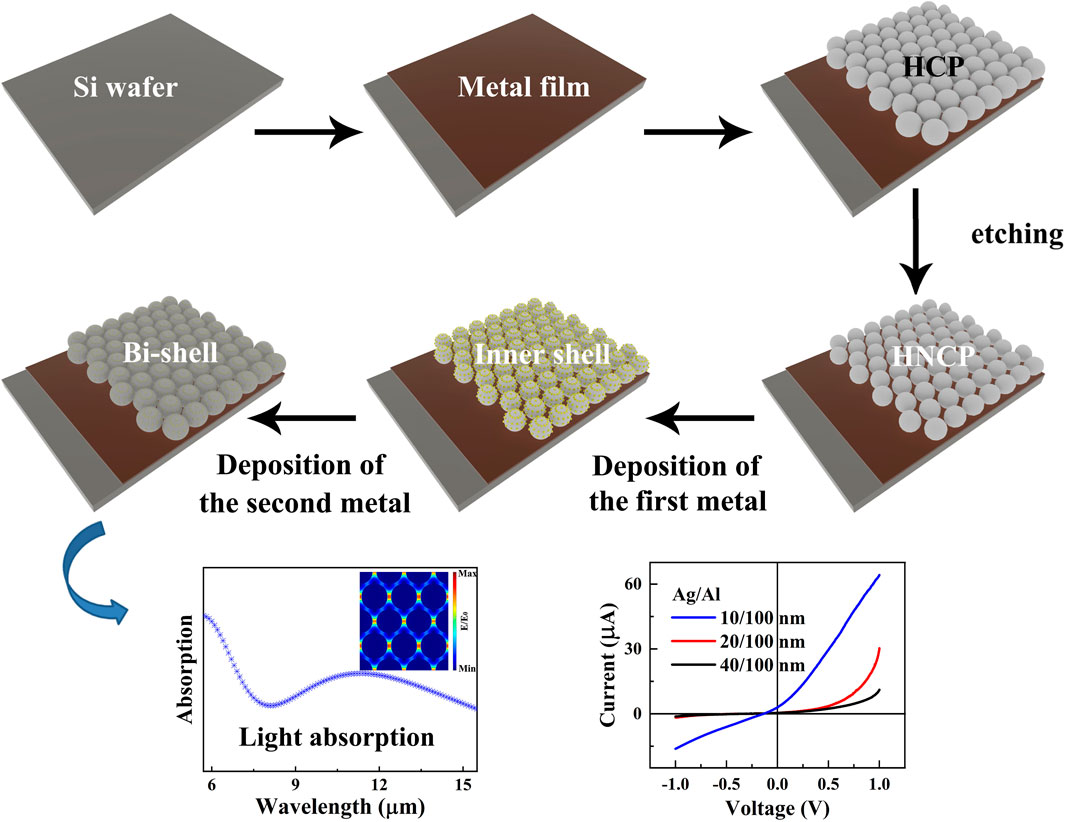
Figure 1. The fabrication process of the sample is illustrated as follows: First, a metal film is deposited on a silicon wafer. Second, a hexagonal close-packed (HCP) polystyrene (PS) sphere template is self-assembled onto the film. Third, etching is used to transform the HCP template into a hexagonal non-close-packed (HNCP) template. Fourth, the first metal is deposited onto the HNCP template. Finally, a second metal is deposited, forming bi-layer metallic arrays. The light absorption peak can be adjusted by selecting the PS sphere diameter. Reproduced with permission (Li et al., 2022), copyright 2022, AIP Publishing. The threshold voltage can modify the thickness of the p-n junction diodes, including the inner and outer shells as well as the bottom film. Reproduced with permission (Li et al., 2023), copyright 2023, John Wiley and Sons.
Thanks to the bi-metallic-shell nanostructure, typical semiconductor behaviors, such as p-type conduction and p-n junction diode characteristics, can be observed when hot carriers dominate current transport. The mobility of hot carriers is approximately 20–40 times higher than that of free electrons. This material with such an exciting phenomenon is referred to as a super-semiconductor (SSC), distinguishing it from traditional semiconductors due to its ultra-low resistivity (∼10−8 Ω m at 300 K, which is 3–10 orders of magnitude lower than that of conventional semiconductors at room temperature) while exhibiting typical semiconductor properties within metals. The bandgap of SSCs is approximately equal to the photon energy (Li et al., 2022), which endows ultra-low-power semiconductor devices.
4 The ballistic transport properties in nanostructured semiconductors
At room temperature, the mean free path of a carrier in devices is approximately 10–20 nm. If the size of a nanodevice is significantly smaller than the mean free path, the scattering probability within the channel becomes negligible. This phenomenon, known as ballistic transport, allows the device current to be entirely controlled by carrier injection from the source into the channel. The limited scattering events during carrier transport substantially reduce heat loss in ballistic transport.
At room temperature, semiconductor carriers frequently scatter with lattice vibrations (phonons) on nanometer and femtosecond scales. This scattering causes electronic energy dissipation, known as Joule heating, and a loss of phase coherence and directionality, imposing significant limitations on the speed and energy efficiency of semiconductor devices. It is noted that the scattering probability is significantly affected by the device size (d) and the mean free path (λ). If d is much larger than λ, diffusive transport dominates, and the current can be well described by conventional mobility theory (Figure 2a). In contrast, when d is much smaller than λ, scattering within the channel becomes negligible. This regime corresponds to ballistic transport, where the device current is governed by carrier injection from the source into the channel (Figure 2b). When d is comparable to λ, the transport behavior falls into the quasi-ballistic regime (Figure 2c).
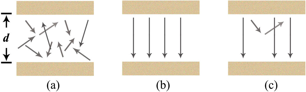
Figure 2. Schematic diagram of ballistic transport. (a) Diffusive transport. The device size d is larger than the mean free path λ. (b) Ballistic transport. The device size d is smaller than the mean free path λ, and the scattering probability in the channel is negligibly small. (c) Quasi-ballistic transport. The device size d is comparable to λ.
Early studies of ballistic transport focused on GaAs materials, which exhibit high mobility at low temperatures (Ruch, 1972; Maloney and Frey, 1977). Recently, with the rise of nanotechnology and two-dimensional materials (Du et al., 2008), transistors featuring room-temperature ballistic transport have garnered significant attention. Ballistic transport in nanostructured devices can significantly reduce thermal losses and enhance energy efficiency, making it a key strategy for improving energy efficiency and environmental sustainability.
5 Comparative analysis
5.1 Plasmon-induced metal-based semiconductors
SSC materials have been explored to construct p-n junction diodes (Ag/Al arrays) with a tunable threshold voltage by simply adjusting the thickness of the inner Ag film. Notably, a near-zero threshold voltage can be achieved with an Ag film approximately 20 nm thick, enabling ultra-low-power p-n junction diodes, resulting in power dissipation of ∼3 W per trillion diodes at a working voltage of 1 V or ∼30 mW per trillion diodes at an operating voltage of 0.1 V (Li et al., 2023), better than that of superconducting diodes, achieved in a superconducting film (MoGe) parrerned with a conformal array of nanoscale holes which typical power dissipation is ∼100 W per trillion diodes at working voltage of 1 mV at 5.75 K (Lyu et al., 2021). Nevertheless, the power dissipation of a diode is of the same order of magnitude as that of a transistor made from the same material. The power consumption of silicon-based transistors is approximately 100 W per 10 billion devices. Therefore, SSCs can reduce power consumption by about three to four orders of magnitude in silicon-based devices, owing to the ultra-low resistivity and high mobility of hot carriers. This ultra-low power consumption fundamentally minimizes the heat dissipation of semiconductor devices, significantly improving their energy efficiency, device performance, and reliability.
Additionally, a built-in electric field in the SSC p-n junction is generated by infrared photons, resulting in a high breakdown field of ∼1.1 × 10⁶ V/cm, comparable to wide-bandgap materials like SiC (2.5 × 10⁶ V/cm) and GaN (2.9 × 10⁶ V/cm) and significantly higher than Si-based materials (3.0 × 10⁵ V/cm). The high breakdown electric field combined with the tuned threshold voltage of the SSC p-n diodes highlights the potential for ultra-low-power semiconducting transistors, integrated circuits, and chips.
5.2 Ballistic transport in nanodevices
Semiconductors can sustain ballistic wave-like energy flows over macroscopic distances at room temperature, enabling ballistic transistors, low-loss energy harvesting, and wave-based information technology. Using Re6Se8Cl2, a van der Waals (vdW) 2-dimensional (2D) nanostructured superatomic semiconductor, Tulyagankhodjaev et al. demonstrated the formation of acoustic exciton-polarons, an electronic quasiparticle shielded from phonon scattering. They directly imaged polaron transport in Re6Se8Cl2 at room temperature, revealing quasi-ballistic, wave-like propagation sustained for a nanosecond and several micrometers using ultrafast stroboscopic scattering microscopy (Tulyagankhodjaev et al., 2023). An above-gap, diffraction-limited visible pump generates excitons, and then a backscattering widefield probe (1.55 eV) slightly below the electronic bandgap spatially resolves how the excitons modify the local polarizability of the material. Shielded polaron transport leads to electronic energy propagation lengths orders of magnitude greater than in other vdW semiconductors, exceeding even silicon over a nanosecond.
Recently, Jiang et al. reported a field-effect transistor (FET) with 2D indium selenide (InSe) with high thermal velocity as channel material that operates at 0.5 V and achieves record high transconductance of 6 mS μm-1 and a room-temperature ballistic ratio in the saturation region of 83%, surpassing those of any reported silicon FETs (Jiang et al., 2023). A yttrium-doping-induced phase-transition method is developed for creating ohmic contacts with InSe, and the InSe FET is scaled down to a channel length of 10 nm. The InSe FETs can effectively suppress short-channel effects, featuring a low subthreshold swing of 75 mV per decade and a drain-induced barrier lowering of 22 mV/V. Furthermore, a low contact resistance of 62 Ω μm is reliably extracted in 10-nm ballistic InSe FETs, resulting in a significantly reduced intrinsic delay and a substantially lower energy-delay product compared to the predicted limit of silicon. Moreover, the 10-nm-gate-length InSe FETs exhibit an energy-delay product of ∼4.32*10−29 Js/μm, one order of magnitude lower than the Si FET limit. The ballistic nanostructured semiconductor transistors could herald an era of essentially lossless nanoelectronics.
6 Challenges and future outlook
It should be noted that the fabrication process for bi-metallic shell arrays, as shown in the schematics in Figure 1, is straightforward and compatible with semiconductor technologies. Therefore, the scalability and reproducibility of the fabrication process are not technically challenging, as evidenced by the ability to control the size and distance of polystyrene sphere templates, as well as the deposition of different bi-metallic pairs (Li et al., 2022; Li et al., 2023). However, it is challenging to obtain defect-free polystyrene sphere templates at the wafer scale, including domain boundaries, voids, size polydispersity, and stacking faults. Uniformity issues can be improved by applying spin coating, substrate tilt for gradient-free assembly, and the Langmuir-Blodgett technique (Xia Y. et al., 2000; Jiang and McFarland, 2004; Kuncicky and Velev, 2008).
Furthermore, SSC devices can be fabricated on immiscible metal films using metal plasmonic resonance materials of various shapes, such as metallic quantum dots (Qi et al., 2023), nanoparticles (Scholl et al., 2012), and nanostructured arrays (Li et al., 2022), when a specialized laser tuned to the plasmon resonance absorption peak is applied. If an SSC device is triggered by infrared light at ambient temperature, the environmental temperature plays a crucial role because the wavelength of infrared light is dependent on temperature. This technology can also be utilized in optoelectronic detectors. Extended to semiconductor chip fabrication, compared with Si-based materials, it can reduce power consumption by approximately 3-4 orders of magnitude due to the ultra-low resistivity and high mobility of hot carriers. Moreover, the hot carriers in SSC devices are influenced by nanostructure or particle size and light illumination rather than voltage, as in traditional semiconductor devices. This unique optical control capability introduces additional flexibility, paving the way for future multifunctional and ultra-low power nanodevice designs.
The ballistic transport property is particularly well-suited for nanodevices with dimensions less than 20 nm in thickness. However, the ballistic transport is sensitive to the monocrystal structure; the existence of defects or impurities will destroy the periodic structure, increase scattering, and reduce the efficiency of ballistic transport in FETs. By minimizing the elastic scattering of carriers, ballistic transport not only significantly reduces thermal losses caused by scattering but also enhances the overall performance of the devices.
In addition, both SSCs and ballistic transport devices are dependent on nanotechnology; in the long term, their stability will be influenced by various factors, including environmental temperature, current heating, oxidation, and atomic diffusion. For example, the SSC arrays are fabricated on polystyrene spheres, and the work temperature is limited to 70 C. Above 50°C, its stability will be severely affected. However, it remains very stable at room temperature, and its rectification performance shows little to no degradation when stored for a year in a dry, room-temperature environment. Furthermore, the reliability of SSC devices at high temperatures will be significantly improved when high-temperature-resistant metal quantum dots are used for preparation.
7 Conclusion
Nanomaterials and nanotechnology will play a crucial role in the development of future energy-efficient electronics. Newly developed nanostructures, such as SSC and quasi/ballistic transport (scattering-free) features in semiconductor devices, drastically reduce energy consumption. Additionally, the high-mobility hot carriers in SSC and the reduced scattering in ballistic transport further enhance device performance. However, these technological advances have led to differences from traditional preparation processes, as well as variations in some intrinsic mechanisms. Similar to the SSC p-n junction, two types of carriers (hot and normal carriers) coexist, resulting in a built-in field and rectification effect that is considerably different from that of traditional semiconductor p-n junctions. The various mechanisms will increase the difficulty of preparing complex SSC semiconductor devices, as they are typically designed based on classical semiconductor theory. It is believed that with the continuous advancement of research into new technologies, the unique nanoscale properties will offer significant advantages for developing EEE, providing performance enhancements and significantly alleviating the current energy consumption dilemma.
Data availability statement
The original contributions presented in the study are included in the article/supplementary material, further inquiries can be directed to the corresponding authors.
Author contributions
ZL: Writing – original draft. BW: Conceptualization, Writing – review and editing.
Funding
The author(s) declare that financial support was received for the research and/or publication of this article. ZL is grateful for the financial support from the National Natural Science Foundation of China (Grants No. 52371197, 51671139) and the Natural Science Foundation of Zhejiang Province (Grant No. LY21F050001).
Conflict of interest
The authors declare that the research was conducted in the absence of any commercial or financial relationships that could be construed as a potential conflict of interest.
Generative AI statement
The author(s) declare that no Generative AI was used in the creation of this manuscript.
Publisher’s note
All claims expressed in this article are solely those of the authors and do not necessarily represent those of their affiliated organizations, or those of the publisher, the editors and the reviewers. Any product that may be evaluated in this article, or claim that may be made by its manufacturer, is not guaranteed or endorsed by the publisher.
References
Behabtu, N., Young, C. C., Tsentalovich, D. E., Kleinerman, O., Wang, X., Ma, A. W. K., et al. (2013). Strong, light, multifunctional fibers of carbon nanotubes with ultrahigh conductivity. Science 339 (116), 182–186. doi:10.1126/science.1228061
Brongersma, M. L., Halas, N. J., and Nordlander, P. (2015). Plasmon-induced hot carrier science and technology. Nat. Nanotech. 10, 25–34. doi:10.1038/NNANO.2014.311
Du, X., Skachko, I., Barker, A., and Andrel, E. Y. (2008). Approaching ballistic transport in suspended graphene. Nat. Nanotech. 3, 491–495. doi:10.1038/nnano.2008.199
Hang, Y. J., Wang, A. Y., and Wu, N. Q. (2024). Plasmonic silver and gold nanoparticles: shape- and structure-modulated plasmonic functionality for point-of-caring sensing, bio-imaging and medical therapy. Chem. Soc. Rev. 53, 2932–2971. doi:10.1039/d3cs00793f
Jiang, P., and McFarland, M. J. (2004). Large-scale fabrication of wafer-size colloidal crystals, macroporous polymers and nanocomposites by spin-coating. J. Am. Chem. Soc. 126, 13778–13786. doi:10.1021/ja0470923
Jiang, J., Xu, L., Qiu, C., and Peng, L. M. (2023). Ballistic two-dimensional InSe transistors. Nature 616, 470–475. doi:10.1038/s41586-023-05819-w
Kang, H., Buchman, J. T., Rodriguez, R. S., Ring, H. L., He, J. Y., Bantz, K. C., et al. (2019). Stabilization of silver and gold nanoparticles: preservation and improvement of plasmonic functionalities. Chem. Rev. 119, 664–699. doi:10.1021/acs.chemrev.8b00341
Kretschmann, E., and Raether, H. (1968). Radiative decay of non-radiative surface plasmons excited by light. Z. Naturforsch. 23A, 2135–2136. doi:10.1515/zna-1968-1247
Kuncicky, D. M., and Velev, O. D. (2008). Surface-guided templating of particle assemblies inside drying sessile droplets. Langmuir 24, 1371–1380. doi:10.1021/la702129b
Kunwar, S., Pandit, S., Jeong, J. H., and Lee, J. (2020). Improved photoresponse of UV photodetectors by the incorporation of plasmonic nanoparticles on GaN through the resonant coupling of localized surface plasmon resonance. Nano-Micro Lett. 12, 91. doi:10.1007/s40820-020-00437-x
Li, Z., Cui, X., Wang, X., Wang, Z., Fang, M., Feng, S., et al. (2022). Plasmon-induced super-semiconductor at room temperature in nanostructured bimetallic arrays. Appl. Phys. Rev. 9, 021412. doi:10.1063/5.0087808
Li, Z., Li, J., Wang, W., Yan, Q., Zhou, Y., Zhu, L., et al. (2023). Near zero-threshold voltage P-N junction diodes based on super-semiconducting nanostructured Ag/Al arrays. Adv. Mat. 35, 2210612. doi:10.1002/adma.202210612
Liu, Y., Xu, G., Ma, D., Li, Z., Yan, Z., Xu, A., et al. (2021). Synergistic effects of g-C3N4 three-dimensional inverse opals and Ag modification toward high-efficiency photocatalytic H2 evolution. J. Clean. Prod. 328, 129745. doi:10.1016/j.jclepro.2021.129745
Lyu, Y. Y., Jiang, J., Wang, Y. L., Xiao, Z. L., Dong, S., Chen, Q. H., et al. (2021). Superconducting diode effect via conformal mapped nanoholes. Nat. Commun. 12, 2703. doi:10.1038/s41467-021-23077-0
Maloney, T. J., and Frey, J. (1977). Transient and steady-state electron transport properties of GaAs and InP. J. . Appl. Phys. 28, 781–787. doi:10.1063/1.323670
Otto, A. (1968). Excitation of nonradiative surface plasma waves in silver by the method of frustrated total reflection. Z. Phys. A Hadrons Nucl. 216, 398–410. doi:10.1007/BF01391532
Qi, M. Y., Tang, Z. R., and Xu, Y. J. (2023). Near field scattering optical model-based catalyst design for artificial photoredox transformation. ACS Catal. 13, 3971–3982. doi:10.1021/acscatal.2c06397
Ruch, J. G. (1972). Electron dynamics in short channel field-effect transistors. IEEE Trans. Electron Devices ED-19, 652–654. doi:10.1109/T-ED.1972.17468
Scholl, J. A., Koh, A. L., and Dionne, J. A. (2012). Quantum plasmon resonances of individual metallic nanoparticles. Nature 483, 421–427. doi:10.1038/nature10904
Shilov, A. (2024). Google and Microsoft consume more power than some countries. Available online at: https://www.tomshardware.com/tech-industry/google-and-microsoft-consume-more-power-than-some-countries.
Spata, V. A., and Carter, E. A. (2018). Mechanistic insights into photocatalyzed hydrogen desorption from palladium surfaces assisted by localized surface plasmon resonances. ACS Nano 12, 3512–3522. doi:10.1021/acsnano.8b00352
Tulyagankhodjaev, J. A., Shih, P., Yu, J., Russell, J. C., Chica, D. G., Reynoso, M. E., et al. (2023). Room-temperature wave-like exciton transport in a van der Waals superatomic semiconductor. Science 382, 438–442. doi:10.1126/science.adf2698
Xia, Y. N., Gates, B., Yin, Y. D., and Lu, Y. (2000). Monodispersed colloidal spheres: old materials with new applications. Adv. Mat. 12, 693–713. doi:10.1002/(sici)1521-4095(200005)12:10<693::aid-adma693>3.3.co;2-a
Keywords: nanotechnology, nanomaterials, energy efficiency electronics, plasmon resonance, ballistic transport
Citation: Li Z and Wei B (2025) Nanotechnology-enabled energy efficiency in semiconductors: plasmon-induced super-semiconductors and ballistic transport devices. Front. Nanotechnol. 7:1560733. doi: 10.3389/fnano.2025.1560733
Received: 14 January 2025; Accepted: 31 July 2025;
Published: 22 August 2025.
Edited by:
Nazmul Hasan, Jashore University of Science and Technology, BangladeshReviewed by:
Suzanna Akil, Université de Lorraine, FranceCopyright © 2025 Li and Wei. This is an open-access article distributed under the terms of the Creative Commons Attribution License (CC BY). The use, distribution or reproduction in other forums is permitted, provided the original author(s) and the copyright owner(s) are credited and that the original publication in this journal is cited, in accordance with accepted academic practice. No use, distribution or reproduction is permitted which does not comply with these terms.
*Correspondence: Zhigang Li, bGl6aGlnYW5nQGlzc3AuYWMuY24=; Bingqing Wei, d2VpYkB1ZGVsLmVkdQ==