 Nicoletta Granchi1,2*
 Richard Spalding3Kris Stokkereit3Matteo Lodde4Maurangelo Petruzzella4Frank V. Otten4
 Riccardo Sapienza5
 Andrea Fiore4
 Marian Florescu3Francesca Intonti1,2
- 1Department of Physics and Astronomy, University of Florence, Sesto Fiorentino, Italy
- 2European Laboratory for Non-Linear Spectroscopy - LENS, University of Florence, Sesto Fiorentino, Italy
- 3Department of Physics, Advanced Technology Institute, University of Surrey, Surrey, United Kingdom
- 4Department of Applied Physics and Science Education, Eindhoven Hendrik Casimir Institute, Eindhoven University of Technology, Eindhoven, Netherlands
- 5The Blackett Laboratory, Department of Physics, Imperial College London, London, United Kingdom
Hyperuniform disordered photonic structures are a peculiar category of disordered photonic heterostructures located between random structures and ordered photonic crystals. These materials, thanks to the presence of a photonic bandgap, exhibit the advantages of random and ordered structures since they have been shown to support in a small spatial footprint a high density of Anderson-localized modes, which naturally occur at the bandgap edges with peculiar features like relatively high Q/V ratios. Different localization behaviors have been recently reported in hyperuniform disordered luminescent materials, with a well-established and widely studied design, based on disordered networks. Here, we explore an alternative design, based on circular holes of different sizes hyperuniformely distributed, that we investigate theoretically and experimentally by means of scanning near-field optical microscopy. We report that the spectral features of hyperuniform disordered networks can also be extended to a different design, which, in turn, displays pseudo-photonic bandgaps and light localization. The ability of generating different kinds of hyperuniform disordered photonic systems that share the same theoretical and experimental optical features can largely extend practical potentialities and integration in many optoelectronic applications.
1 Introduction
Recently, disordered dielectric heterostructures with structural correlations, which fill the gap between random structures and photonic crystals, have attracted a lot of attention (Yu et al., 2020) (Vynck et al., 2021). A particular class among disordered photonic materials is called hyperuniform disordered (HuD) photonic structures (Torquato, 2018; Torquato and Stillinger, 2003). A point pattern in real space is hyperuniform if, within a spherical sampling window of radius
2 Materials and methods
2.1 Theoretical design
The 2D hyperuniform disordered photonic structure is generated under periodic boundary conditions in a square of side
2.2 Sample fabrication
The sample was grown by molecular-beam epitaxy on a GaAs (001) wafer and consists of two GaAs membranes separated by a Al0.7Ga0.3As sacrificial layer, on top of a Al0.7Ga0.3As sacrificial layer (Joannopoulos et al., 2011; Midolo and Fiore, 2014; Petruzzella et al., 2016; Petruzzella et al., 2017). High-density InAs quantum dots (QDs) are embedded in the middle of the upper membrane and act as an optically active medium. The photoluminescence (PL) emission of the QDs ranges from 1,100 to 1,350 nm. The HuD structure was defined by electron-beam lithography, reactive-ion etching, and subsequent selective etching of the sacrificial layers. The slab thickness and the intermembrane separation distance are, respectively, t = 130 nm and d = 105 nm (details on the scanning electron microscopy (SEM) investigation on similar samples are given in Granchi et al. (2022).
2.3 Finite element method simulations
To simulate the 3D structure along with its optical properties, we use finite element method (FEM) simulations through the commercial software application COMSOL Multiphysics (Zobenica et al., 2017) to obtain information on the eigenvalues and eigenvectors of the system. The double-membrane structure was simulated by modeling one membrane and then imposing perfect electric conductor (PEC) conditions in the plane between the two membranes in order to detect antisymmetric solutions.
2.4 Scanning near-field optical microscopy
A commercial SNOM (Twinsnom, Omicron) is used in illumination/collection geometry. The spatially resolved optical maps were recorded by scanning the probe tip over the sample at a fixed distance (few tens of nm). The sample is excited by a laser diode at 785 nm, both the excitation and the signal collection occur through the tip, and the collected signal is dispersed using a spectrometer and collected by a cooled InGaAs array. At every tip position, the entire spectrum of the sample is collected with a spectral resolution of 0.1 nm. The SNOM tip-collecting area, which has a lateral size of about 250 nm, is the estimated spatial resolution of our system.
3 Results and discussion
The 2D design of the HuD pattern under study, containing
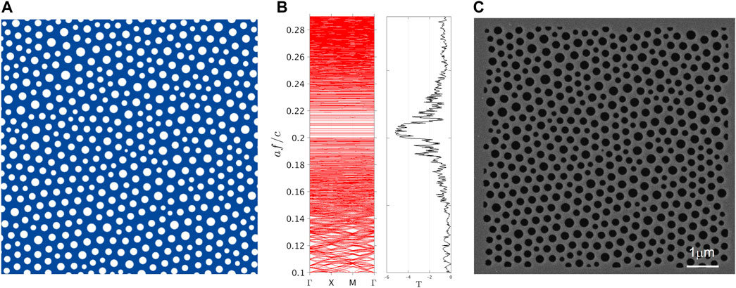
FIGURE 1. (A) Sketch of the theoretical design of the studied hyperuniform disordered network, which constitutes the elementary cell, with the length scale
We fabricated the samples (details on fabrication can be found in Section 2) based on the HuD design of Figure 1A. The samples consist in two GaAs parallel membranes patterned with air circular holes, following the theoretical design. Vertical etching ensures that the hole patterns in the two parallel membranes have the same nominal design. Interestingly, double-membrane photonic systems have been recently proposed as promising devices for sensing and metrology applications, for the possibility that they offer the possibility of achieving a deterministic control of the supported coupled modes (Midolo and Fiore, 2014; Petruzzella et al., 2016; Petruzzella et al., 2017; Batten et al., 2008; Balestri et al., 2019). By patterning the double membranes with the HuD design, we simply include HuD systems into the large plethora of practical applications, which focus on post-fabrication control of photonic modes. A top view SEM image of the fabricated sample, where only the upper membrane is visible, is reported in Figure 1C, along with a zoom on the patterned area and with a sketch of the double membrane system. The structural parameters are reported in Section 2.2.
When using a double-membrane system, the symmetry of the problem leads to the splitting into symmetric and antisymmetric modes, which are vertically delocalized over the two membranes. It has been proven both theoretically and experimentally that the modes arising from the coupling between parallel membranes inherit the in-plane spatial distributions of the modes supported by the original single membrane (Balestri et al., 2019). For this reason, the results here presented can also be extended to single-membrane structures. For the sake of simplicity, we focus only on antisymmetric solutions.
Previous works highlighted that photonic HuD systems support a variety of transport regimes and a photonic band gap (Florescu et al., 2009; Degl'Innocenti et al., 2016). Specifically, Anderson-localized modes with relatively high Q factors occur naturally at the PBG edges and are predicted to spread over a few cells of HuD structures (Granchi et al., 2019; COMSOL, 2019). These modes are distinguishable as below or above the PBG due to the electric field being concentrated in the dielectric or air fraction, respectively. As the modes step away from the PBG, they enter a diffusive regime and consequently spatially spread over the entire structure and exhibit lower Q factors (Granchi et al., 2022). Here, we study the localization of Anderson modes arising in the pseudo-gap region at the lower edge of a small PBG and concentrated in the dielectric part of the sample. To explore the localization properties of these modes, we calculate the (antisymmetric) solutions of the 3D double-membrane HuD system by means of FEM simulations. A sketch of the simulation domain, in which we exploit the mirror symmetry of the system to simulate only half of the structure, is shown in Figure 2A (Section 2.3). For each eigensolution obtained with FEM simulations, we extract the central wavelength, spectral width, and electric field amplitude of the modes supported by the HuD system. With these data, we can reconstruct the spectrum of the system by representing every mode with a Lorentzian curve with every single-mode wavelength, spectral bandwidth, and amplitude, and plotting them as a function of wavelength. The resulting spectrum, which is reported in Figure 2A, exhibits a high density of modes, a feature which is typical of disordered systems. The yellow band highlights the presence of the small PBG since no mode is detected in that spectral window. Many peaks are present in the spectrum, with Q factors ranging from 200 to 3,000. Around
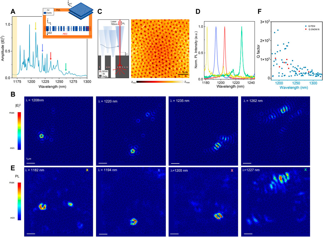
FIGURE 2. (A) Spectrum of the system reconstructed through Lorentzian curves plotted with central wavelength, spectral width, and amplitude obtained with FEM simulations. The yellow bar highlights the presence of the photonic band gap (PBG). A sketch of the simulated model is shown on the upper right side. (B) FEM maps of the electric field intensity of four dielectric modes (
We select a few solutions, distinguishable for the peculiar and localized spatial profile, and plot the corresponding electric field intensity spatial distribution in Figure 2B. The modes are spectrally located around
In order to experimentally characterize light localization at the lower PBG edge of the sample, we employed a room temperature SNOM in an illumination-collection geometry (Figure 2C). Details on the experimental setup can be found in Section 2. In our experimental setup, spatially resolved optical maps are recorded by scanning the probe tip over the sample at a fixed distance (few tens of nm). This technique allows performing hyper-spectral imaging (HSI), that is, we collect a full spectrum of the photonic local density of states (LDOS) of a system for any spatial pixel of the near-field map. This allows reconstructing hyperspectral maps that can either be filtered around a single wavelength, for example, the central wavelength of a single peak, or around a broad spectral interval. Moreover, during the scan, a topographical map is recorded simultaneously with the acquisition of the optical signal. The topography of the studied sample is reported on the right of Figure 2C. We performed a 10
An important aspect of HuD modes is the mode predictability for the design and their robustness against fabrication-induced disorder (Granchi et al., 2022). Here, we address this matter by performing SNOM measurement on two nominally identical samples that we label as Replica 1 and Replica 2. We investigate the two replicas and demonstrate that the same modes can be observed in the two samples as a confirmation of recently shown results based on simulations regarding the mode robustness to fabrication-induced disorder (Rumi et al., 2019). Some examples of the reproducible modes are given in Figure 3. In particular, we exploit the combination of the near-field HSI technique with the topographic imaging of the samples to align different maps at the nanoscale. Moreover, for every tip position, we calculate the PL enhancement spectrum by dividing the recorded near-field spectrum by one of the QDs (Granchi et al., 2022). In this way, it is possible to also reconstruct PL enhancement maps. In Figure 3A, we report the PL enhancement spectra acquired at the position of maximum intensity of the PL signal of the selected mode in the replica (in blue), compared with respect to its counterpart in the original structure (in red). Correspondingly, the panels of Figure 3B show the SNOM PL enhancement maps acquired at the central wavelengths of the red peaks in Replica 1, respectively, λ = 1,183.6 nm, λ = 1,196.0 nm, λ = 1,205.0 nm, and λ = 1,263.0 nm. In Figure 3C, we show instead the SNOM PL maps acquired at the central wavelengths of the blue peaks in Replica 2, respectively, λ = 1,179.9 nm, λ = 1,196.0 nm, λ = 1,206.0 nm, and λ = 1,265.4 nm. The similarity of the submicrometric details of the most variable shapes in the field distributions of the replicas is evident for all the four considered modes, not only in the brightest spots but also throughout the zones with a lower signal. Notably, the first three considered modes are strongly localized and exhibit a very high PL enhancement factor well reproduced in both replicas, and this reaches a maximum value of
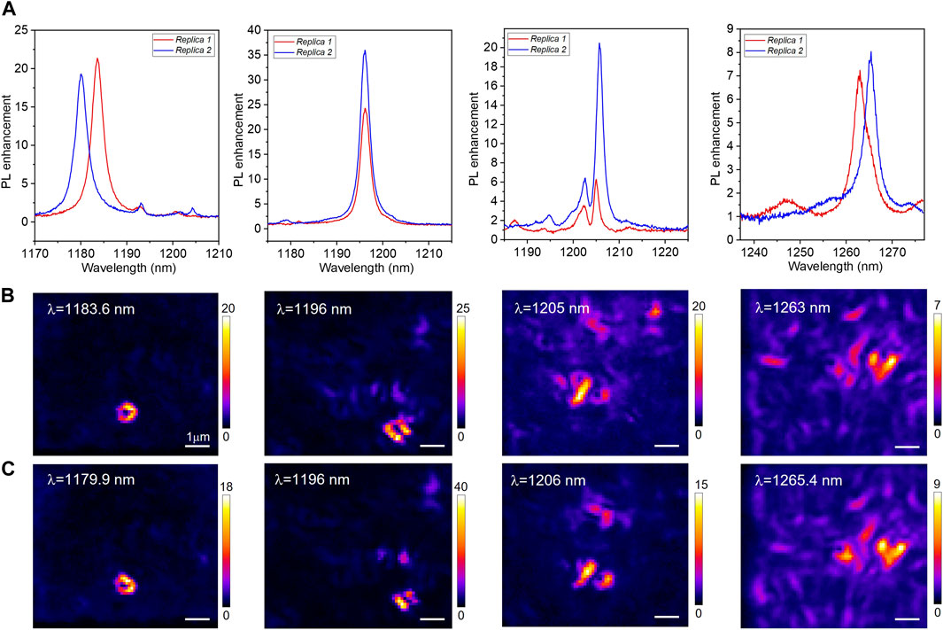
FIGURE 3. (A) PL enhancement spectra of four different modes acquired in the point of maximum intensity of each. The spectra of Replica 1 are represented in red, and those of Replica 2 are represented in blue. Panels in (B,C) are the SNOM PL enhancement maps filtered around the central wavelengths of the red (blue) peaks in Replica 1 (Replica 2), specifically λ = 1,183.6 nm (λ = 1,179.9 nm), λ = 1,196.0 nm (λ = 1,196.0 nm), λ = 1,205.0 nm (λ = 1,205.0), and λ = 1,263.0 nm (λ = 1,265.4).
4 Conclusion
In conclusion, in this work, we explored light localization features in HuD luminescent materials in an alternative design exploiting circular holes of different sizes in a HuD pattern. By means of theoretical simulations and SNOM HSI, we have predicted and detected the formation of the high density of Anderson-localized modes at the pseudo-gap lower edge, featuring Q factors of the order of 103. Our analysis shows that these modes exhibit a high degree of robustness against the fabrication-induced disorder and that they share this feature also with delocalized resonances spectrally far from the pseudo-gap and relative to a diffusive regime of light transport. The ability of generating different kinds of hyperuniform disordered photonic systems that supports modes sharing the same optical features might constitute a step toward the inclusion of hyperuniform materials into promising platforms for optoelectronic applications.
Data availability statement
The original contributions presented in the study are included in the article/Supplementary Material. Further inquiries can be directed to the corresponding author.
Author contributions
NG conducted the experiments, numerical simulations, and contributed to the writing of the manuscript, and the interpretation of results. RSp and KS conducted numerical simulations and designed the structure. ML and MP fabricated the semiconductor structure. FI and MF supervised the work and contributed to the writing of the manuscript and interpretation of the results. AF and RSa contributed to the supervision of the work. All authors contributed to the article and approved the submitted version.
Funding
FI acknowledges funding provided by PNRR project I-PHOQS (CUP B53C22001750006).
Conflict of interest
The authors declare that the research was conducted in the absence of any commercial or financial relationships that could be construed as a potential conflict of interest.
Publisher’s note
All claims expressed in this article are solely those of the authors and do not necessarily represent those of their affiliated organizations, or those of the publisher, the editors, and the reviewers. Any product that may be evaluated in this article, or claim that may be made by its manufacturer, is not guaranteed or endorsed by the publisher.
References
Anderson, P. W. (1958). Absence of diffusion in certain random lattices. Phys. Rev. 109, 1492–1505. doi:10.1103/physrev.109.1492
Aubry, G. J., Froufe-Pérez, L. S., Kuhl, U., Legrand, O., Scheffold, F., and Mortessagne, F. (2020). Experimental tuning of transport regimes in hyperuniform disordered photonic materials. Phys. Rev. Lett. 125, 127402. doi:10.1103/physrevlett.125.127402
Balestri, D., Petruzzella, M., Checcucci, S., Intonti, F., Caselli, N., Sgrignuoli, F., et al. (2019). Mechanical and electric control of photonic modes in random dielectrics. Adv. Mater. 31, 1807274. doi:10.1002/adma.201807274
Batten, R. D., Stillinger, F. H., and Torquato, S. (2008). Classical disordered ground states: Super-ideal gases and stealth and equi-luminous materials. J. Appl. Phys. 104, 033504. doi:10.1063/1.2961314
Castro-Lopez, M., Gaio, M., Sellers, S., Gkantzounis, G., Florescu, M., and Sapienza, R. (2017). Reciprocal space engineering with hyperuniform gold disordered surfaces. Apl. Photonics 2, 061302. doi:10.1063/1.4983990
COMSOL (2019). Multiphysics. Available at: www.comsol.com.
Degl’Innocenti, R., Shah, Y. D., Masini, L., Ronzani, A., Pitanti, A., Ren, Y., et al. (2016). Hyperuniform disordered terahertz quantum cascade laser. Sci. Rep. 6, 19325. doi:10.1038/srep19325
Florescu, F., Torquato, S., and Steinhardt, P. J. (2009). Designer disordered materials with large, complete photonic band gaps. Proc. Natl. Acad. Sci. 106, 20658–20663. doi:10.1073/pnas.0907744106
Florescu, M., Steinhardt, P. J., and Torquato, S. (2013). Optical cavities and waveguides in hyperuniform disordered photonic solids. Phys. Rev. B 87, 165116. doi:10.1103/physrevb.87.165116
Froufe-Pérez, L. S., Engel, M., Damasceno, P. F., Muller, N., Haberko, J., Glotzer, S. C., et al. (2016). Role of short-range order and hyperuniformity in the formation of band gaps in disordered photonic materials. Phys. Rev. Lett. 117, 053902. doi:10.1103/physrevlett.117.053902
Froufe-Pérez, L. S., Engel, M., Sáenz, J. J., and Scheffold, F. (2017). Band gap formation and Anderson localization in disordered photonic materials with structural correlations. PNAS 114 (36), 9570–9574. doi:10.1073/pnas.1705130114
Gerasimenko, Y. A., Vaskivskyi, I., Litskevich, M., Ravnik, J., Vodeb, J., Diego, M., et al. (2019). Quantum jamming transition to a correlated electron glass in 1T-TaS2. Nat. Mater. 18, 1078–1083. doi:10.1038/s41563-019-0423-3
Granchi, N., Fagiani, L., Salvalaglio, M., Barri, C., Ristori, A., Montanari, M., et al. (2023). Engineering and detection of light scattering directionalities in dewetted nanoresonators through dark-field scanning microscopy. Opt. Express 31, 9007. doi:10.1364/oe.481971
Granchi, N., Lodde, M., Stokkereit, K., Spalding, R., van Veldhoven, P. J., Sapienza, R., et al. (2023). Near-field imaging of optical nanocavities in hyperuniform disordered materials. Phys. Rev. B 107, 064204. doi:10.1103/physrevb.107.064204
Granchi, N., Montanari, M., Ristori, A., Khoury, M., Bouabdellaoui, M., Barri, C., et al. (2021). Near-field hyper-spectral imaging of resonant Mie modes in a dielectric island. Apl. Photonics 6, 126102. doi:10.1063/5.0070626
Granchi, N., Petruzzella, M., Balestri, D., Fiore, A., Gurioli, M., and Intonti, F. (2019). Multimode photonic molecules for advanced force sensing. Opt. Express 27, 37579. doi:10.1364/oe.27.037579
Granchi, N., Spalding, R., Lodde, M., Petruzzella, M., Van Otten, F., Fiore, A., et al. (2022). Near-field investigation of luminescent hyperuniform disordered materials. Adv. Opt. Mater. 10, 2102565. doi:10.1002/adom.202102565
Haberko, J., Froufe-Pérez, L. S., and Scheffold, F. (2020). Transition from light diffusion to localization in three-dimensional amorphous dielectric networks near the band edge. Nat. Commun. 11, 4867. doi:10.1038/s41467-020-18571-w
Intonti, F., Vignolini, S., Riboli, F., Vinattieri, A., Wiersma, D. S., Colocci, M., et al. (2008). Spectral tuning and near-field imaging of photonic crystal microcavities. Phys. Rev. B 78, 041401. doi:10.1103/physrevb.78.041401
Johnson, S., and Joannopoulos, J. (2001). Block-iterative frequency-domain methods for Maxwell's equations in a planewave basis. Opt Express 8, 173. doi:10.1364/oe.8.000173
Kuznetsov, A. I., Miroshnichenko, A. E., Fu, Y. H., Zhang, J., and Luk'yanchuk, B. (2012). Magnetic light. Sci. Rep. 2, 492. doi:10.1038/srep00492
Liu, W., and Kivshar, Y. S. (2018). Generalized Kerker effects in nanophotonics and meta-optics [Invited]. Opt. Express 26, 13085. doi:10.1364/oe.26.013085
Midolo, L., and Fiore, A. (2014). Design and optical properties of electromechanical double-membrane photonic crystal cavities. IEEE J. Quantum Electron. 50, 404–414. doi:10.1109/jqe.2014.2315873
Milošević, M. M., Man, W., Nahal, G., Steinhardt, P. J., Torquato, S., Chaikin, P. M., et al. (2019). Hyperuniform disordered waveguides and devices for near infrared silicon photonics. Sci. Rep. 9, 20338. doi:10.1038/s41598-019-56692-5
Mitchell, N. P., Nash, L. M., Hexner, D., Turner, A. M., and Irvine, W. T. M. (2018). Amorphous topological insulators constructed from random point sets. Nat. Phys. 14, 380–385. doi:10.1038/s41567-017-0024-5
Muller, N., Haberko, J., Marichy, C., and Scheffold, F. (2013). Silicon hyperuniform disordered photonic materials with a pronounced gap in the shortwave infrared. Adv. Opt. Mater. 2, 115–119. doi:10.1002/adom.201300415
Petruzzella, M., La China, F., Intonti, F., Caselli, N., De Pas, M., van Otten, F. W. M., et al. (2016). Nanoscale mechanical actuation and near-field read-out of photonic crystal molecules. Phys. Rev. B 94, 115413. doi:10.1103/physrevb.94.115413
Petruzzella, M., Pagliano, F. M., Zobenica, Ž., Birindelli, S., Cotrufo, M., van Otten, F. W. M., van der Heijden, R. W., et al. (2017). Electrically driven quantum light emission in electromechanically tuneable photonic crystal cavities. Appl. Phys. Lett. 111, 251101. doi:10.1063/1.5008590
Piechulla, P. M., Muehlenbein, L., Wehrspohn, R. B., Nanz, S., Abass, A., Rockstuhl, C., et al. (2018). Fabrication of nearly-hyperuniform substrates by tailored disorder for photonic applications. Adv. Opt. Mater. 6, 1701272. doi:10.1002/adom.201701272
Rumi, G., Sánchez, J. A., Elı́as, F., Maldonado, R. C., Puig, J., Bolecek, N. R. C., et al. (2019). Hyperuniform vortex patterns at the surface of type-II superconductors. Phys. Rev. Res. 1, 033057. doi:10.1103/physrevresearch.1.033057
Salvalaglio, M., Bouabdellaoui, M., Bollani, M., Benali, A., Favre, L., Claude, J.-B., et al. (2020). Hyperuniform monocrystalline structures by spinodal solid-state dewetting. Phys. Rev. Lett. 125, 126101. doi:10.1103/physrevlett.125.126101
Tavakoli, N., Spalding, R., Lambertz, A., Koppejan, P., Gkantzounis, G., Wan, C., et al. (2022). Over 65% sunlight absorption in a 1 μm Si slab with hyperuniform texture. ACS Photonics 9, 1206–1217. doi:10.1021/acsphotonics.1c01668
Torquato, S. (2018). Hyperuniform states of matter. Phys. Rep. 745, 1–95. doi:10.1016/j.physrep.2018.03.001
Torquato, S., and Stillinger, F. H. (2003). Local density fluctuations, hyperuniformity, and order metrics. Phys. Rev. E 68, 041113. doi:10.1103/physreve.68.041113
Vynck, K., Pierrat, R., Carminati, R., Froufe-Pérez, L. S., Scheffold, F., Sapienza, R., et al. (2021). Light in correlated disordered media.
Yu, S, Qiu, C.-W, Chong, Y., Torquato, S., Park, N., and Park, N. (2020). Engineered disorder in photonics. Nat. Rev. Mater. 6, 226–243. doi:10.1038/s41578-020-00263-y
Zhou, W., Cheng, Z., Zhu, B., Sun, X., and Tsang, H. K. (2016). Hyperuniform disordered network polarizers. IEEE J. Sel. Top. Quantum Electron. 22, 1–294. doi:10.1109/jstqe.2016.2537270
Keywords: near-field, hyperuniform, nano-optics, correlated disorder, light localization, Anderson
Citation: Granchi N, Spalding R, Stokkereit K, Lodde M, Petruzzella M, Otten FV, Sapienza R, Fiore A, Florescu M and Intonti F (2023) High spatial resolution imaging of light localization in hyperuniform disordered patterns of circular air pores in a dielectric slab. Front. Photonics 4:1199411. doi: 10.3389/fphot.2023.1199411
Received: 03 April 2023; Accepted: 18 May 2023;
Published: 14 June 2023.
Edited by:
Michele Ortolani, Sapienza University of Rome, ItalyReviewed by:
Simone Zanotto, National Research Council (CNR), ItalyAlfredo De Rossi, Thales Group (France), France
Copyright © 2023 Granchi, Spalding, Stokkereit, Lodde, Petruzzella, Otten, Sapienza, Fiore, Florescu and Intonti. This is an open-access article distributed under the terms of the Creative Commons Attribution License (CC BY). The use, distribution or reproduction in other forums is permitted, provided the original author(s) and the copyright owner(s) are credited and that the original publication in this journal is cited, in accordance with accepted academic practice. No use, distribution or reproduction is permitted which does not comply with these terms.
*Correspondence: Nicoletta Granchi, Z3JhbmNoaUBsZW5zLnVuaWZpLml0