 Mengfa Wang1†
 Yiming Wang1†Jun Qian1Zhaolin Li1Wenhui Xue1Victor Qi2Xijian Zhang1Haotian Ling3Gongbin Tang4Qingpu Wang1
 Aimin Song1,5Chao Cao1*
 Yifei Zhang1*
- 1School of Integrated Circuit, Shandong University, Jinan, China
- 2Design Center of AKMMV, Guangzhou, China
- 3QiLu Aerospace Information Research Institute, Jinan, China
- 4State Key Laboratory of Crystal Materials, Shandong University, Jinan, China
- 5Department of Electrical and Electronic Engineering, University of Manchester, Manchester, United Kingdom
In this work, a four-port directional filter (DF) with a broad passband and low reflection is proposed at the W-band, which comprises three unit filters at 92, 95, and 97 GHz, cascaded in series. Each unit consists of two microstrip lines in the top circuit layer for signal input and output, two pairs of apertures in the middle ground layer for directional coupling, and one square loop in the bottom layer as a selective resonator. By sweeping the working frequencies of the three units and optimizing the phase delays between them, the proposed filter achieves a 3-dB bandwidth as broad as 16%, an insertion loss of 2.5 dB at 95 GHz, and an out-of-band rejection of −28 and −23 dB at 80 and 110 GHz, respectively. The corresponding reflection attenuation is larger than 9.6 dB from 60 to 105 GHz. To verify our design, a prototype is fabricated and characterized, and its experimental data are consistent with the simulation. This work significantly expands the bandwidth of DFs and may find many applications in frequency division multiplexing and high-gain wireless systems.
1 Introduction
Filters are the most important components in microwave and optical systems to get the desired signals and suppress unwanted noises (Asci et al., 2020; Wu et al., 2020; Wu et al., 2021). Typically, the noises are strongly reflected back to the input port (Baqir et al., 2019). Directional filters (DFs) are a kind of four-port filter with little reflection in the input port. In ideal conditions, wideband signals fed into port 1 do not travel to port 4 or reflect back to port 1, the desired bands travel to port 3, and the rest of the spectra travel to port 2. This unique property is beneficial to eliminate the undesired oscillation induced by the filter out-of-band reflection in high-gain and high-power systems (Zhang et al., 2018). In addition, they can act either as channel combiners or channel dividers in frequency division multiplexing (Coale, 1958; Wang et al., 2022). The initial DFs were developed in bulky and heavy waveguides at microwave frequencies, which typically show a bandwidth of less than 2% due to the high Q-factor of metal waveguide (Cameron and Yu, 1958). To get a low profile and small weight, planar standing-wave and traveling-wave DFs were proposed on printed circuit boards (PCBs) in the range of several GHz (Cohn and Coale, 1956; Zinka et al., 2003; Kim, 2011; Lobato-Morales et al., 2011; Lobato-Morales et al., 2013). For the former, two standing-wave resonators with carefully designed phase configurations between them can guide the desired signals to a certain port, which can provide a bandwidth of less than 5% (Cohn and Coale, 1956; Zinka et al., 2003; Kim, 2011; Lobato-Morales et al., 2011; Lobato-Morales et al., 2013). The latter, with loop resonators and two quarter-wavelength directional couplers, also achieves several percent bandwidths, which is similar to their standing-wave counterparts (Coale, 1956; Walker, 1978; Uvasl, 1997; Uvsal, 2003; Cheng et al., 2007; Sarkar et al., 2007). As the frequency increases to the millimeter wave (mmW) range, the aforementioned planar DF structures suffer from weak coupling between the feed lines and resonators and, thus, the large insertion loss in their passband. To overcome this obstacle, large coupling capacitors between the vertically overlapped electrodes in multilayer circuits have been investigated for mmW DFs (Cohn and Coale, 1956; Tanaka et al., 1988; Uvsal, 2003; Sarkar et al., 2007). Unfortunately, the bandwidth of multilayer DFs is still limited to several percent. In our previous work, a novel traveling-wave DF with dual-slot directional couplers achieved a 3-dB bandwidth of 8%, which, to our knowledge, is state of the art (Zhang et al., 2017). In summary, it should be noted that the resonant units of the reported DFs are designed at the same frequencies for consistent phase configurations (Cameron and Yu, 2011; Lobato-Morales et al., 2011; Lobato-Morales et al., 2013; Kim, 2011; Zinka et al., 2003; Cohn and Coale, 1956; Coale, 1956; Uvasl, 1997; Cheng et al., 2007; Walker, 1978; Uvsal, 2003; Sarkar et al., 2007; Tanaka et al., 1988; Zhang et al., 2017).
To obtain advanced functionalities at mmW frequencies, many wireless systems desire broadband. For instance, broadband can provide a high data transmission rate to communication and high detection contrast to imaging (Nakasha et al., 2009; Tian et al., 2022). As a relative term, broadband may be considered as >15% in many applications, such as multiple-input and multiple-output (MIMO) communication and distributed array imaging systems (Soszka, 2022; Martin et al., 2015). In addition to the bandwidth, gain and output power are of great importance in the above systems in the mmW realm. Typically, mmWs address higher atmospheric and circuit attenuations than low microwaves (Martin et al., 2015). In this case, mmW front-end modules require high gain and high power to compensate for the attenuations, which may easily induce stability problems, such as self-oscillation, with the strong out-of-band reflection of the traditional two-port filters (Zhang et al., 2018). On the other hand, PCB circuit elements and microwave monolithic integrated circuit (MMIC) chips become sub-wavelength and easily produce near-field radiation and mutual coupling at mmW frequencies, further damaging the system’s stability. In this regard, broadband DFs with little reflection are urgently desired for the aforementioned advanced wireless systems at mmW frequencies.
In this paper, we propose a broadband DF with little reflection in multilayer LCP circuits at the W-band, achieving a 3-dB bandwidth of 16%. A new design method is induced for the broadband DFs by using resonant units at various frequencies. Differing from the classic DFs with the identical resonant units, the proposed DF consists of three filter units at 92, 95, and 97 GHz, which are cascaded in a carefully optimized order. It achieves a low insertion loss of 2.5 dB at 95 GHz and a large return loss of >9.6 dB at the E- and W-band. This paper is organized as follows. In Section 2, we introduce the brief design principles of the multilayer DFs with directional couplers, the detailed design methods of the broadband DFs with various filter units, and their optimization. In Section 3, the proposed DFs are fabricated and characterized, and their measured data are analyzed and compared with the other reported DFs. In the end, the conclusion and acknowledgment are given.
2 Design and analysis
Multilayer DFs with one-loop resonator and two quarter-wavelength directional couplers are promising candidates for mmW applications, as shown in Figure 1A, which was first reported in our previous work (Zhang et al., 2017). Two parallel microstrip lines with four ports are designed in the top circuit layer, which couple to the loop resonator in the bottom circuit layer through the dual-slot quarter-wavelength coupler in the middle circuit layer. Port 1 and port 4 are the input and isolated ports, respectively, and port 2 and port 3 are for the undesired spectra and filtering signal, respectively. The equivalent circuit model of this filter is given in Figure 1B. C′ represents the coupling capacitance between the top and the bottom microstrip lines, and C11 and C21 are the capacitors between the microstrip line and the ground plane due to the coupling slots. L11, L21, L22, and L23 depict the various phase delays on the microstrip lines. By optimizing the phase configuration of the directional coupler and loop resonator, in-phase signals are added in port 3, and out-of-phase signals are added in port 4.
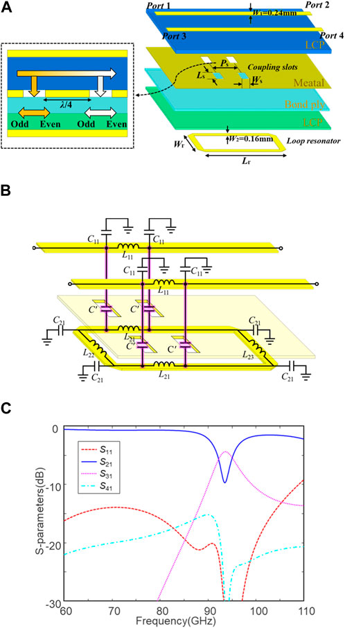
FIGURE 1. Directional filter unit in multilayer LCP circuits. (A) 3D configuration of one filter unit with two dual-slot directional couplers, (B) its equivalent circuit model, and (C) the simulated S-parameters of one unit designed at 94 GHz.
The substrate used in this work is liquid crystal polymer (LCP), which has a low dielectric constant of 3.2, a low loss tangent of 0.004 at the W-band, and a low water-absorption rate of 0.04% (Zhang et al., 2017; Zhou et al., 2022). The metal cladding is 15-μm copper. The Ansys high-frequency structure simulator (HFSS), i.e., a commercial electromagnetic simulator with a finite element method, is employed for 3D full-wave simulation. In the following, we discuss the design principles of the DF unit and investigate broadband DFs by cascading DF units in series.
2.1 Filter unit design
The main contribution of this work is not the design of the filter unit so that we just discuss the brief working mechanism. The slot coupling between the top and bottom lines excites weak odd and even modes with opposite propagating directions and similar magnitude. Two slots with π/4 phase delay form a directional coupler, where the odd modes are out-of-phase and canceled, and the even modes are in phase and added, as shown in the inset of Figure 1A. The DF unit is composed of two directional couplers and one loop resonator. By distributing L11, L21, L22, and L23 as π/4, π/4, π/2, and π, respectively, the desired spectra are directionally filtered into port 3, as illustrated in Figure 1C. The design and optimization details can be found in our previous work (Zhang et al., 2017).
Here, the filter units at 92, 95, and 97 GHz are designed for the cascaded DFs in the following sections, the dimensions of which are shown in Table 1 and the simulated passbands of which are shown in Figure 2. It can be seen that the bandwidth of a filter unit ranges from 92.6 GHz to 97.6 GHz, i.e., a fractional bandwidth of only 5.5%, the insertion loss (|S31|) is around 4.6 dB in the passband, and the reflection attenuation (|S11|) is larger than 10 dB at the W-band. As can be seen in Figure 1C, the through loss (|S21|) is less than 10 dB in one filter unit so that cascading filter units can enlarge the through loss and reduce the insertion loss.
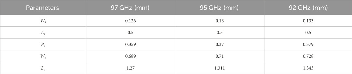
TABLE 1. Dimensions of the designed DF units at different frequencies.
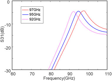
FIGURE 2. Simulated passband curves of the filter units at 92, 95, and 97 GHz.
2.2 DFs with the identical units cascaded in series
As discussed above, one DF unit cannot sufficiently filter the desired signals, having large insertion loss (|S31|) and small through loss (|S21|) at the resonant frequency. In this section, we will discuss how to suppress the insertion loss and broaden the bandwidth by cascading filter units.
First, a two-stage DF with the identical units is investigated as the simplest example, as shown in Figure 3A. Port 1 and port 3 of the second unit connect to port 2 and port 4 of the first unit, respectively. Due to the symmetry of the device, the S-parameters of the first unit satisfy the following relations (Pozar, 2012):
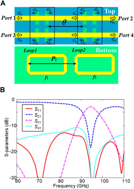
FIGURE 3. Cascaded DF with two filter units at 95 GHz. (A) Configuration of the two-stage DF and (B) the simulated S-parameters of a two-stage DF with the identical units at 95 GHz.
S21 and S41 of the first unit feed the second unit as the input. The transmission can be described by the following formula (Zhang et al., 2017):
where
Next, a three-stage DF with identical units is investigated based on the above analysis of the two-stage DF, as illustrated in Figure 4A. In addition, the high-order terms of
where θ′ is the phase delay between the second and third units. ST’ 31 is maximum at θ = nπ and θ' = mπ (m and n are integers), and the corresponding Pr and Pʹr are chosen as 1.9 mm. Figure 4B illustrates the simulated S-parameters of the three-stage DF. It can be seen that the insertion loss |S31| is reduced to 2.6 dB, and the through loss |S21| is increased to 26 dB at 95 GHz. The 3-dB bandwidth is broadened up to 10.2%. The main contribution factors are S1 21, θ, and θ'.
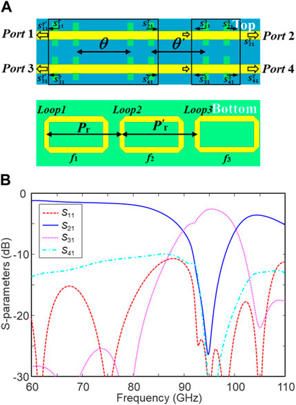
FIGURE 4. Cascaded DF with three filter units at 95 GHz. (A) Configuration of the three-stage DF and (B) the simulated S-parameters of a three-stage DF with the identical units at 95 GHz.
Adding more filter units can further increase the bandwidth slightly. However, due to the increasing through loss |S21|, this approach is limited. Figure 5A illustrates the simulated S-parameters of a four-stage DF with the identical units at 95 GHz, whose bandwidth is slightly increased to 11.3%. The bandwidth and insertion loss performances of the cascaded DFs with respect to the filter unit numbers are shown in Figure 5B and Table 2. The DFs can achieve lower insertion loss and wider bandwidth at a cost of unit numbers and device profile. However, the improved efficiency reduces significantly as the unit number increases.
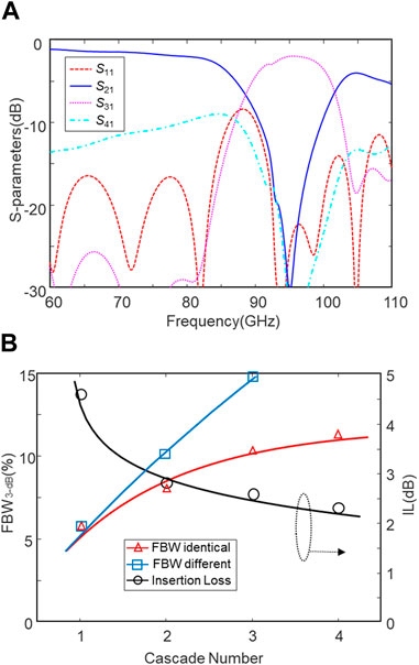
FIGURE 5. Cascaded DFs with the identical units at 95 GHz. (A) Simulated S-parameters of a cascaded DF with four identical units and (B) the bandwidth and insertion loss with respect to the unit numbers.
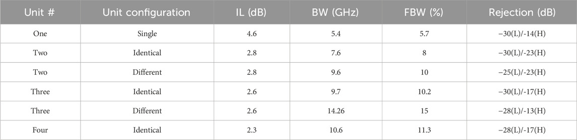
TABLE 2. Insertion loss, bandwidth, and out-of-band rejection of the designed DFs.
2.3 DFs with different units cascaded in series
In the reported DF designs, all resonant units are designed at the same frequency to get consistent phase configuration (Cameron and Yu, 2011; Lobato-Morales et al., 2011; Lobato-Morales et al., 2013; Kim, 2011; Zinka et al., 2003; Cohn and Coale, 1956; Coale, 1956; Uvasl, 1997; Cheng et al., 2007; Walker, 1978; Uvsal, 2003; Sarkar et al., 2007; Tanaka et al., 1988; Zhang et al., 2017). In contrast, classic Chebyshev-type filters may use resonant units designed at adjacent frequencies to broaden the filter bandwidth (Pozar, 2012). In this section, this approach will be investigated in the cascaded DFs to broaden the passband for the first time.
First, a two-stage DF with different units is investigated, whose configuration is illustrated in Figure 3A. Empirically, the insertion loss of filters and propagation loss of microstrip lines increase as the frequency increases. To compensate the dispersive loss and achieve broadband, the filter units are cascaded in an order from high to low frequency. The second filter unit is designed at f2 = 95 GHz, and the frequency of the first unit f1 sweeps from 99 to 95 GHz. Pr remains 1.9 mm initially, as in the last section. Figure 6A illustrates the simulated S-parameters with various f1, where the bandwidth enlarges as f1 increases. However, a transmission dip occurs between f1 and f2 as these two resonant frequencies diverge, which may damage the bandwidth. Therefore, f1 is chosen as 97 GHz to suppress the dip. Next, the phase delay θ and pitch Pr are swept for optimization according to Equations 2.3a, 2.3b, 2.3c, and 2.3d, as shown in Figure 6B. As Pr gets smaller, the bandwidth gets larger, and the transmission dip gets stronger. In this case, Pr is chosen as 1.85 mm. The simulated S-parameters of the optimized two-stage DF with different units are illustrated in Figure 6C. The 3-dB bandwidth of the passband is increased to 10%, which is similar to the three-stage DF with the identical units. The insertion loss (|S31|) is 2.6 dB at 96 GHz, and the corresponding through loss (|S21|) is around 17 dB.
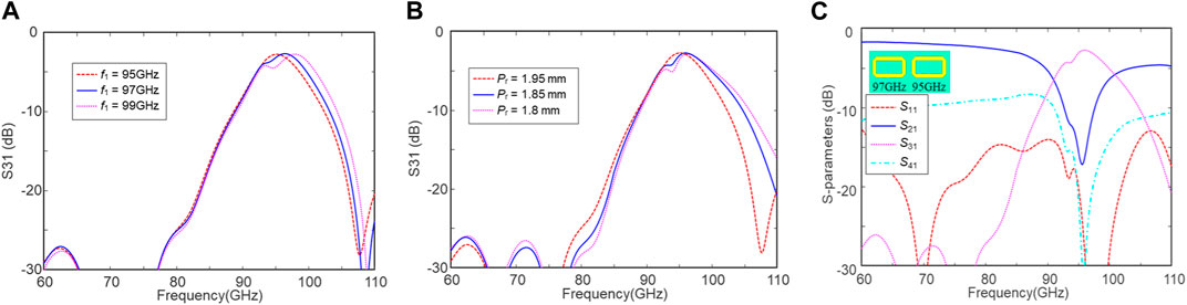
FIGURE 6. Simulated S-parameters of a two-stage DF with different units at 97 and 95 GHz. (A) Sweeping the frequency of the first unit f1, (B) sweeping the pitch Pr between the first and second units, and (C) simulated S-parameters of the optimized two-stage DF.
Then, we investigate a three-stage DF with different units based on the above two-stage DF with 97-GHz and 95-GHz units. To broaden the bandwidth and suppress the transmission dip, the third filter unit is designed at f3 = 92 GHz, whose dimensions can be found in Table 1. Initially, Pr remains 1.85 mm, and Pʹr is set as 1.9 mm. According to Eq. 2.4, both θ and θ′ affect the passband, so we need to optimize both Pr and Pʹr. Figure 7A illustrates the simulated S-parameters with various Pʹr. As Pʹr increases, the passband red shifts and enlarges slightly. However, a transmission dip will be induced at large Pʹr, which may damage the bandwidth. In this case, Pʹr is chosen as 1.7 mm to compensate the bandwidth and transmission dip. Next, parameter variation of Pr is studied again, which is shown in Figure 7B. Smaller Pr leads to the blue shift of the passband and a stronger transmission dip between f2 and f3. To avoid strong transmission dips, both Pr and Pʹr are optimized as 1.7 mm. Finally, the simulated S-parameters of the optimized three-stage DF are illustrated in Figure 7C. The insertion loss (|S31|) is 2.6 dB at 95 GHz, and the out-of-band attenuation is −20 dB at 85 and −13 dB at 110 GHz, respectively. The 3-dB bandwidth of S31 is 14.26 GHz, and the corresponding fractional bandwidth is 15% centered at 95 GHz, which is significantly improved using different filter units.
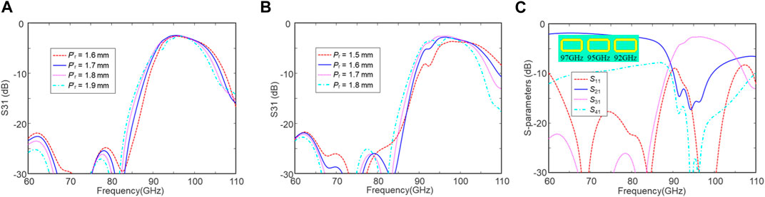
FIGURE 7. Simulated S-parameters of a three-stage DF with different units at 97, 95, and 92 GHz. (A) Sweeping pitch P′r between the second and third units, (B) sweeping pitch Pr between the first and second units, and (C) simulated S-parameters of the optimized three-stage DF.
2.4 Filter order and insertion loss analysis
As comparison, a three-stage DF with 95-, 97-, and 92-GHz units cascaded in series is investigated, whose S-parameters are illustrated in Figure 8. The unit pitch Pr and Pʹr are kept at 1.7 mm. With respect to Figure 7C, the high-frequency performance of S31 is sacrificed significantly. The bandwidth of the passband is significantly reduced to 11%, which is similar to the three-stage DF with the identical units, and the insertion loss is slightly reduced to 2.4 dB. Therefore, it should be concluded that the first unit is more dominant for the cascaded DF design and is more important for high frequencies. The second filter unit has an input signal around 3-dB smaller than the first unit; see S21 at 97 GHz in Figure 1C. The bandwidth and insertion loss parameters of the proposed DFs with various units are listed in Table 2. On using different filter units, the bandwidth of the three-stage DF is much larger than that of the four-stage DF with the identical units. In contrast, the different filter units show little loss discrepancy to the identical filter units.
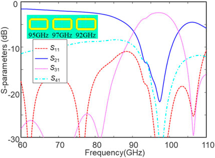
FIGURE 8. Simulated S-parameters of a three-stage DF with different DFs cascaded in the order of 95–97–92 GHz. The bandwidth is just 11%.
As can be seen in Table 2, the insertion loss can be minimized by cascading filter units, which shows decreasing efficiency at large unit numbers. The propagation loss of microstrip lines on a 100-μm LCP substrate is 0.156 dB/mm, and the averaged radiation loss is approximately 0.065 dB/mm in the loop resonator (Zhang et al., 2017). In this case, the absolute insertion loss induced by each directional coupler is just around 0.8 dB. The main contributing factor for the insertion loss of the cascaded DF is the wave propagation loss on the microstrip lines, which is induced by the loss tangent of the LCP substrate and leaky radiation.
3 Experiment
To verify the optimized design, a prototype was fabricated in AKM Electronics Industrial (PanYu) Ltd. Low-temperature LCP films with a melting temperature of 290°C were utilized for multilayer lamination. Figure 9A illustrates the fabricated device. Long meandered microstrip lines and ground–signal–ground (G–S–G) probe pads are carefully designed for launching G–S–G probes and providing enough space for mmW absorbers. The design details of the probe pads can be found in our previous paper (Zhang et al., 2016). Table 3 compares the fabricated dimensions and the designed dimensions, revealing good fabrication tolerances. The discrepancies are typically less than 10 μm.
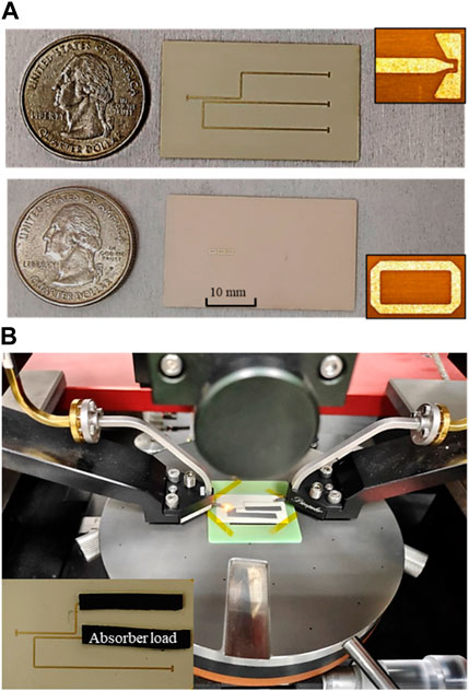
FIGURE 9. (A) Fabricated three-stage DF with 97-, 95-, and 92-GHz filter units, G–S–G probe pads, and meandered microstrip lines and (B) its measurement setup with the absorbers on the meandered microstrip lines as good load.
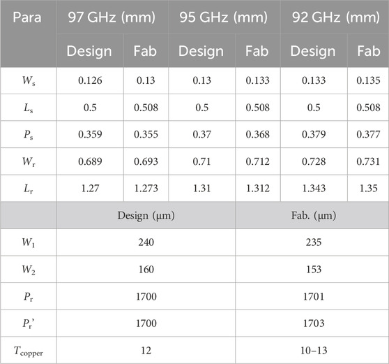
TABLE 3. Dimensions of the fabricated three-stage DF with various filter units.
The measurement system setup is illustrated in Figure 9B. G–S–G probes integrated with Keysight programmable network analyzer N5247 are launched on the probe pads for signal input and output, and RF absorbers are attached onto the other ports for loading. A 10-mm-long absorber can provide a large reflection attenuation of 15 dB, which is sufficient for the DF test (Zhang et al., 2017). Before the test, the probes were calibrated with the short-open-load-through (SOLT) method using a CS-5 calibration substrate from GGB Industries Inc. The measurement spectrum is from 70 to 110 GHz due to the W-band waveguide. The insertion losses of the probe pads and meandered MSLs were eliminated from the characterized S-parameters by using cascaded scattering matrices for a good match between the measured and simulated data. The derivation details can be found in the work of Zhang et al. (2017).
The characterized S-parameters of the fabricated three-stage DFs are illustrated in Figure 10. The reflection loss (|S11|) is larger than 11 dB from 70 to 110 GHz, revealing a perfect little-reflection performance in an ultra-wideband. The through loss (|S21|) shows three resonances at 95, 97, and 99 GHz, which are slightly higher than the design due to the fabrication tolerances and non-perfect absorber loads. The insertion loss (|S31|) is 2.86 dB at 98 GHz, which is slightly higher than the simulated data, and the out-of-band rejection is 28 and 23 dB at 80 and 115 GHz, respectively. The isolation loss (|S41|) is also larger than 10 dB at the W-band. It should be noted that the 3-dB passband is as large as 15.7 GHz, which corresponds to a fractional bandwidth of 16%. Table 4 compares the proposed device with the other reported DFs. The proposed device has the highest working frequency and the widest bandwidth. In addition, it addresses reasonable insertion loss and return loss. The device size is 1.3 mm × 6 mm, i.e., 0.4 λ × 1.9 λ at 95 GHz.
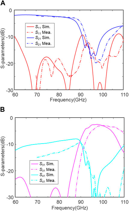
FIGURE 10. Measured and simulated S-parameters of the fabricated three-stage DF at the W-band. (A) S11 and S21 and (B) S31 and S41.
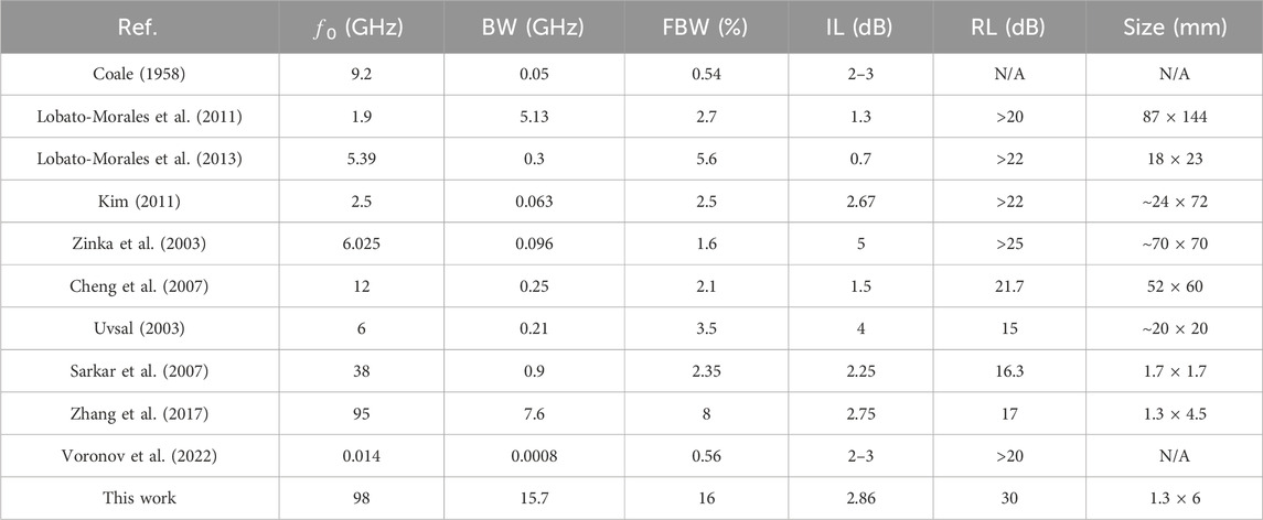
TABLE 4. Comparison of this work and the other reported directional filters.
4 Conclusion
A broadband DF with three filter units at 97, 95, and 92 GHz cascaded in series in multilayer LCP substrates is designed, fabricated, and characterized. Each DF unit consists of two microstrip lines in the top circuit layer for signal input and output, two directional couplers in the second ground layer, and one square loop resonator in the third layer. A new design method with resonant units at various frequencies is discussed for DFs. By optimizing the working frequencies of the three units and sweeping the pitches between them, the proposed DF achieves a 3-dB bandwidth of 16% at 98 GHz, an insertion loss of as low as 2.6 dB, and an out-of-band rejection of 28 and 23 dB at 80 and 115 GHz, showing reasonable agreement with the simulated data. The bandwidth is state of the art according to our knowledge. Such a device may find promising applications in broadband frequency division multiplexers and high-gain systems at mmW frequencies.
Data availability statement
The original contributions presented in the study are included in the article/Supplementary material; further inquiries can be directed to the corresponding authors.
Author contributions
MW: writing–original draft, investigation, project administration, resources, validation, and writing–review and editing. YW: writing–review and editing, data curation, validation, and writing–original draft. JQ: writing–review and editing, methodology, and supervision. ZL: writing–review and editing and conceptualization. WX: writing–review and editing, investigation, and supervision. VQ: formal analysis, methodology, and writing–review and editing. XZ: methodology, writing–review and editing, formal analysis, and funding acquisition. HL: writing–review and editing, investigation, methodology, and project administration. GT: writing–review and editing, data curation, and supervision. QW: project administration, writing–review and editing, methodology, and validation. AS: writing–review and editing, data curation, and project administration. CC: investigation, methodology, supervision, writing–original draft, and writing–review and editing. YZ: conceptualization, funding acquisition, investigation, supervision, validation, visualization, writing–original draft, and writing–review and editing.
Funding
The authors declare that financial support was received for the research, authorship, and/or publication of this article. This work was supported by the National Key Research and Development Program of China (2022YFA1405200), the National Natural Science Foundation of China (62371272), the Natural Science Foundation Major Fundamental Program of Shandong Province (ZR2023ZD08), the Key Research and Development Program of Shandong Province (2019JZZY020109), and the Key Region Program of Shandong Province (2203-370322-89-01-562763).
Acknowledgments
The authors would like to thank the Multidisciplinary Precision Oncology Project of Shandong University and the Center of Nanoelectronics of Shandong University for supporting this work.
Conflict of interest
The authors declare that the research was conducted in the absence of any commercial or financial relationships that could be construed as a potential conflict of interest.
Publisher’s note
All claims expressed in this article are solely those of the authors and do not necessarily represent those of their affiliated organizations, or those of the publisher, the editors, and the reviewers. Any product that may be evaluated in this article, or claim that may be made by its manufacturer, is not guaranteed or endorsed by the publisher.
References
Asci, C., Sadeqi, A., Wang, W., Nejad, H. R., and Sonkusale, S. (2020). Design and implementation of magnetically–tunable quad–band filter utilizing split–ring resonators at microwave frequencies. Sci. Rep. 10 (1050), 1050. doi:10.1038/s41598-020-57773-6
Baqir, M. A., Choudhury, P. K., Fatima, T., and Ibrahim, A.-B. M. A. (2019). Graphene-over-graphite-based metamaterial structure as optical filter in the visible regime. Sci. Opt. 180, 832–839. doi:10.1016/j.ijleo.2018.12.005
Cameron, R. I., and Yu, M. (2011). Design of manifold-coupled multiplexers. IEEE Microw. Mag. 8 (5), 46–59. doi:10.1109/MMM.2007.904715
Cheng, Y., Hong, W., and Wu, K. (2007). Half mode substrate integrated waveguide (HMSIW) directional filter. IEEE Microw. Wirel. Compon. Lett. 17 (7), 504–506. doi:10.1109/lmwc.2007.899309
Coale, F. S. (1956). A traveling-wave directional filter. IRE Trans. Microw. Theory Techn. 4 (4), 256–260. doi:10.1109/TMTT.1956.1125073
Coale, F. S. (1958). Applications of directional filters for multiplexing systems. IRE Trans. Microw. Theory Techn. 6 (4), 450–453. doi:10.1109/TMTT.1958.1125223
Cohn, S. B., and Coale, F. S. (1956). Directional channel-separation filters. Proc. IRE. 44 (8), 1018–1024. doi:10.1109/JRPROC.1956.275043
Kim, J. (2011). Improved design of single-section and cascaded planar directional filters. IEEE Trans. Microw. Theory Techn. 59 (9), 2206–2213. doi:10.1109/TMTT.2011.2160871
Lobato-Morales, H., Corona-Chavez, A., Itoh, T., and Olvera-Cervantes, J. L. (2011). Dual-band multi-pole directional filter for microwave multiplexing applications. IEEE Microw. Wirel. Compon. Lett. 21 (12), 643–645. doi:10.1109/LMWC.2011.2172683
Lobato-Morales, H., Sun, J. S., Corona-Chavez, A., Itoh, T., and Olvera-Cervantes, J. L. (2013). Novel microstrip diplexer for ultra-wideband (UWB) and wireless LAN (WLAN) bands. J. Electromagn. Waves Appl. 27 (11), 1338–1350. doi:10.1080/09205071.2013.808598
Martin, R. D., Shi, S., Zhang, Y., Wright, A., Yao, P., Shreve, K. P., et al. (2015). Video rate passive millimeter-wave imager utilizing optical upconversion with improved size, weight, and power. Proc. SPIE. 9462, 946209. doi:10.1117/12.2177133
Nakasha, Y., Sato, M., Tajima, T., Kawano, Y., Suzuki, T., Takahashi, T., et al. (2009). $W$-band transmitter and receiver for 10-Gb/s impulse radio with an optical-fiber interface. IEEE Trans. Microw. Theory Techn. 57 (12), 3171–3180. doi:10.1109/TMTT.2009.2033242
Sarkar, S., Pinel, S., Kidera, N., and Laskar, J. (2007). Analysis and application of 3-D LTCC directional filter design for multiband millimeter-wave integrated module. IEEE Trans. Adv. Packag. 30 (1), 124–131. doi:10.1109/TADVP.2006.890206
Soszka, M. (2022). Fading channel predication for 5G and 6G mobile communication systemsInt. J. Electron. Commun. 68 (1), 153–160. doi:10.24425/ijet.2022.139863
Tanaka, T., Tsunoda, K., and Aikawa, M. (1988). Slot-coupled directional couplers between double-sided substrate microstrip lines and their applications. IEEE Trans. Microw. Theory Techn. 26 (12), 1752–1757. doi:10.1109/22.17410
Tian, X., Chang, T., and Cui, H. (2022). Short-range millimeter-wave imaging in the presence of array element position deviation. IEEE Trans. Microw. Theory Techn. 70 (3), 1910–1919. doi:10.1109/TMTT.2022.3142165
Uysal, S. (1997). Microstrip loop directional filter. Electron. Lett. 33 (6), 475–476. doi:10.1049/el:19970313
Uysal, S. (2003). Multilayer microstrip loop directional filter. Proc. SBMO/IEEE MTT-S Int. Microw. Optoelectron. Conf. (IMOC). 1, 25–29. doi:10.1109/IMOC.2003.1244826
Voronov, A., Syms, R. R. A., and Sydoruk, O. (2022). High-performance magnetoinductive directional filters. Electronics 15 (6), 845. doi:10.3390/electronics11060845
Walker, J. L. B. (1978). Exact and approximate synthesis of TEM-mode transmission-type directional filters. IEEE Trans. Microw. Theory Techn. 26 (3), 186–192. doi:10.1109/TMTT.1978.1129342
Wang, M., Zhang, B., Li, Z., Wang, Y., Guo, Q., Liu, W., et al. (2022). Frequency division multiplexer with directional filters in multilayer LCP films at - and -Band<i/> <i/>. IEEE Microw. Wirel. Compon. Lett. 32 (11), 1287–1290. doi:10.1109/LMWC.2022.3177606
Wu, F., Wu, J., Fan, C., Guo, Z., Xue, C., Jiang, H., et al. (2020). Omnidirectional optical filtering based on two kinds of photonic band gaps with different angle-dependent properties. EPL 129 (3), 34004. doi:10.1209/0295-5075/129/34004
Wu, F., Zhang, Z., Yin, C., and Chen, G. (2021). Omnidirectional narrow-band ultraviolet filtering based on one-dimensional defective photonic crystal containing hyperbolic metamaterial. Sci. Phys. B 608, 412872. doi:10.1016/j.physb.2021.412872
Zhang, Y., Martin, R. D., Shi, S., Wright, A., Yao, P., Shreve, K., et al. (2018). 95-GHz front-end receiving multichip module on multilayer LCP substrate for passive millimeter-wave imaging. IEEE Trans. Compon. Packag., Manuf. Technol. 8 (12), 2180–2189. doi:10.1109/TCPMT.2018.2805708
Zhang, Y., Shi, S., Martin, R. D., and Prather, D. W. (2016). Substrate integrated waveguide filter on LCP substrate at 94 GHz. Microw. Opt. Technol. Lett. 58 (3), 577–580. doi:10.1002/mop.29621
Zhang, Y., Shi, S., Martin, R. D., and Prather, D. W. (2017). Broadband SIW-to-Waveguide transition in multilayer LCP substrates at W-band. IEEE Microw. Wirel. Compon. Lett. 27 (3), 224–226. doi:10.1109/LMWC.2017.2661716
Zhang, Y., Shi, S., Martin, R. D., and Prather, D. W. (2017). Slot-coupled directional filters in multilayer LCP substrates at 95 GHz. IEEE Trans. Microw. Theory Techn. 65 (2), 476–483. doi:10.1109/TMTT.2016.2615929
Zhang, Y., Wang, F., Shi, S., Martin, R. D., Yao, P., and Prather, D. W. (2017). Ultra-wideband microstrip line-to-microstrip line transition in multilayer LCP substrate at millimeter-wave frequencies. IEEE Microw. Wirel. Compon. Lett. 27 (10), 873–875. doi:10.1109/LMWC.2017.2747125
Zhou, Z., Li, W., Qian, J., Liu, W., Wang, Y., Zhang, X., et al. (2022). Flexible liquid crystal polymer technologies from microwave to Terahertz frequencies. Molecules 27 (4), 1336. doi:10.3390/molecules27041336
Keywords: broadband, directional filter, liquid crystal polymer, low reflection, multilayer circuit
Citation: Wang M, Wang Y, Qian J, Li Z, Xue W, Qi V, Zhang X, Ling H, Tang G, Wang Q, Song A, Cao C and Zhang Y (2024) Broadband directional filter in multilayer liquid crystal polymer films at W-band. Front. Photonics 5:1364883. doi: 10.3389/fphot.2024.1364883
Received: 03 January 2024; Accepted: 27 February 2024;
Published: 11 March 2024.
Edited by:
Ikmo Park, Ajou University, Republic of KoreaReviewed by:
Haitao Jiang, Tongji University, ChinaMuhammad Abuzar Baqir, COMSATS University Islamabad, Sahiwal campus, Pakistan
Copyright © 2024 Wang, Wang, Qian, Li, Xue, Qi, Zhang, Ling, Tang, Wang, Song, Cao and Zhang. This is an open-access article distributed under the terms of the Creative Commons Attribution License (CC BY). The use, distribution or reproduction in other forums is permitted, provided the original author(s) and the copyright owner(s) are credited and that the original publication in this journal is cited, in accordance with accepted academic practice. No use, distribution or reproduction is permitted which does not comply with these terms.
*Correspondence: Yifei Zhang, eWlmZWl6aGFuZ0BzZHUuZWR1LmNu; Chao Cao, Y2hhb19jYW9Ac2R1LmVkdS5jbg==
†These authors have contributed equally to this work