 Emanuele Smecca1
 Ajay Kumar Jena2
 Ioannis Deretzis1
 Salvatore Valastro1,3
 Salvatore Sanzaro1Giovanni Mannino1Corrado Bongiorno1
 Antonino La Magna1Tsutomu Miyasaka2
 Alessandra Alberti1*
- 1CNR-IMM, Zona Industriale, Catania, Italy
- 2Graduate School of Engineering, Toin University of Yokohama, Yokohama, Japan
- 3Dipartimento di Fisica e Astronomia, Università di Catania, Catania, Italy
Hybrid perovskites are one of the most popular materials nowadays due to their very exclusive properties. To mitigate costs, complexity, and environmental impact, in this work, we have prepared methylammonium lead iodide (MAPbI3) films by a two-step Low-Vacuum Proximity-Space-Effusion (LV-PSE). The LV-PSE method exploits the low vacuum and the short diffusion path from the precursor source to have high thermal energy and partial pressure of the sublimated species close to the substrate. To this aim, the substrate is located at a medium distance (∼2 cm) from the melting pots in a low-vacuum chamber at ∼4 × 10⁻² mbar. In the first step, a PbI2 film is deposited on a substrate; in the second step, the conversion into MAPbI3 occurs via an adsorption-incorporation-migration mechanism through the evaporation of methylammonium iodide (MAI) reagents. To exploit the potential of the conversion reaction, 190 nm MAPbI3 layers are deposited on TiO2 substrates. The layers were characterized in terms of crystal structure by X-ray diffraction (XRD) analyses, which showed the exclusive presence of MAPbI3 confirming the complete conversion of the PbI2 film. Scanning Electron Microscopy (SEM) analyses revealed a flat uniform pinhole-free coverage of the substrates and good conformational coverage of the TiO2 underlayer. Transmission Electron Microscopy (TEM) analyses addressed the formation of the tetragonal phase and the absence of the amorphous phase in the film. Spectroscopic ellipsometry (SE) analyses were used to explore the optical properties and the stability of the MAPbI3 layer at different temperatures and ambient conditions. As proof of concept, solar cell architectures were prepared using TiO2 as Electron Transporting Layer (ETL), Spiro-OMeTAD as Hole Transporting Layer (HTL), and Au as a contact to exploit the new up-scalable and clean deposition method. Using just ∼190 nm thick layers, the best efficiency reached with this architecture was 6.30%.
Introduction
With the continuous increase in energy consumption worldwide and the need for low carbon emission, the demand for renewable energy is nowadays one of the hottest topics in the world community. In this perspective, solar energy conversion is one the most promising technologies as attested by the increase of the installed capacity in the last decade that goes from 41.145 MW in 2010 to 707.494 MW in 2020, increasing from ∼3.3% to ∼25.75% of the total renewable energy installed, which constitutes a major contribution among all the renewable energy technologies (IRENA 2021).
In the photovoltaic research scenario, hybrid perovskites have emerged as a promising technology with rapid efficiency improvement. From the first application in 2009 (Kojima et al., 2009), in just 10 years, hybrid perovskites solar cells (PSC) were able to reach a remarkable efficiency of 25.5% (National Renewable Energy Laboratory (NREL), 2021). Some issues, such as poor stability in humid air (Smecca et al., 2016; Deretzis et al., 2018), the development of large-area deposition processes, are slowing down their commercialization. For large-area deposition, the use of spin coating (Eperon et al., 2014), with some variation like the antisolvent (Jeon et al., 2014) or the two-step deposition methods (Burschka et al., 2013) where the PbI2 is spin-coated and then the substrate is dipped into a methylammonium iodide (MAI) solution or even the two-step spin coating technique where both films are deposited by spin coating (Im et al., 2014), is proven to be the best technique in terms of laboratory-scale devices but is unlikely to be used for the industrial-scale production.
A good solution to this problem is provided by vacuum deposition techniques. Liu et al. (2013) have first demonstrated the feasibility of vacuum co-deposition of CH3NH3PbI3 (MAPbI3) films. An efficiency of 20.8%, which is the highest efficiency for vacuum-deposited perovskite so far, has been achieved by Perez Del Rey et al. (2018) using an n-i-p architecture with organic Electron Transporting Layer (ETL) and Hole Transporting Layer (HTL), with 890 nm thick MAPbI3 films that were deposited by co-evaporation of MAI and PbI2 at high vacuum. Another remarkable result was reached by Li et al. (2020), who reported a 20.3% efficiency using ∼500 nm active MAPbI3 layer treated with Potassium Acetate and MAI solution after the deposition, with a relatively complicated architecture (FTO/SnO2/TiO2/Phenyl-C61-butyric acid methyl ester (PCBM)/MAPbI3-treated/2,20,7,70-tetrakis-(N,N-di-4-methoxyphenylamino)-9, 90-spirobifluorene (Spiro-OMeTAD)/Au). In both works, the use of an organic ETL layer over the inorganic oxide layer was necessary to improve the I-V characteristic of the device. One of the known issues with evaporated MAPbI3 is their low performance when coupled with inorganic electron transporting layers (ETL) such as TiO2 (Patel et al., 2017; Kerner and Rand, 2017) with respect to the use of organic ETLs. Cojocaru et al. (2018) have demonstrated that a thin layer of PCBM over the inorganic ETL noticeably improves the device performance by reducing hysteresis and improving Voc, Jsc, and Fill factor. They have attributed the improvements to better adhesion between the organic PCBM underlayer and the MAPbI3 film with respect to the TiO2/MAPbI3 interfaces. Chemical vapor deposition (CVD) is one of many other vapor deposition methods developed to prepare MAPbI3 on TiO2 to avoid solution process techniques. Leyden et al. (2014) have used a high-vacuum chemical vapor deposition (HV-CVD) to prepare 300 nm of the active layer in a two-step process in two different chambers using PbCl2 as a precursor. Luo et al. (2015) have developed a Low-pressure Chemical Vapor Deposition (LV-CVD) technique to prepare a 500 nm MAPbI3 layer that produced an efficiency of 12.8% when used in a perovskite solar cell. In both cases, the use of a carrier gas increases the complexity of the equipment and process optimization. Most importantly, the use of complex systems increases the cost of the overall deposition technology. Other deposition techniques were developed using mixed vacuum-solution processed steps. Chen et al. (2014) have developed the Vapor-Assisted Solution Process (VASP) where a spin-coated PbI2 film was converted into MAPbI3 by exposing the PbI2 film to MAI vapor rather than MAI solution, thus obtaining 12.1% efficiency with 350 nm MAPbI3 film. Guo et al. (2016) have used a closed space sublimation technique to convert a previously solution-processed PbI2 film into MAPbI3 by the sublimation of MAI powder in close proximity to the substrate (mm). In this respect, it can be noticed that the combination of different techniques for the deposition increases complexity, costs, and time for the device’s preparation, making them not industrially appealing.
To mitigate the costs and complexity of vacuum methods, we explored a fully solvent-free technique called Low-Vacuum Proximity-Space-Effusion (LV-PSE) (Smecca et al., 2021) for the deposition of MAPbI3 film on TiO2 substrate. This technique uses a two-step approach where a first PbI2 layer is first deposited by vacuum evaporation and is subsequently converted into MAPbI3 in the same chamber without any vacuum breaking. The LV-PSE method exploits the low vacuum and the short diffusion path to generate high energy and high partial pressure of the evaporated species in the region close to the substrate. With respect to high-vacuum techniques, this combination sets advantageous kinetics on the substrate with a major impact on the material quality and reduces the process time and cost, making it a suitable process for industrial application. The films deposited were investigated in terms of crystal (XRD and TEM), morphology (SEM and TEM), and optical properties (SE). The I-V characteristics of proof-of-concept devices were tested, showing an efficiency for LV-PSE deposited film of 6.3% in the reverse scan for a cell using just ∼190 nm thick layer of MAPbI3.
Materials and Methods
Perovskite Film Preparation
The MAPbI3 films were deposited by specifically customized vacuum deposition equipment provided by Kenosistec s.r.l. Lead iodide powders (99.99% purity) and purchased from Sigma Aldrich. Methylammonium iodide was purchased from Dyenamo AB. All materials were used as received without any further purification. The growth method is fully described in our previous work (Smecca et al., 2021) and consists of a sequential deposition of PbI2 and MAI via physical sublimation from powders at a base pressure of ∼2 × 10⁻² mbar with the crucibles taken at 350°C and 135°C, respectively. The substrate temperatures during the PbI2 deposition step and MAI deposition step were ∼120°C and ∼75°C, respectively.
Device Preparation
First, FTO substrates were cleaned with a soap solution (Hellmanex™), then acetone, and finally distilled water. A TiO2 compact layer of 50 nm thickness was prepared by spin coating (3,000 rpm, 30 s) a diluted solution of titanium diisopropoxide bis(acetylacetonate) {i.e., [Ti (acac)2 (iPrO)2]} (75 wt%, Aldrich) in ethanol [100 ml Ti (acac) + 1 ml EtOH] two times with 10 min of drying at 120°C between the first and the second coating. Then, the precursor-coated FTO substrates were dried at 120°C again for 10 min before sintering them at 500°C for 1 h in a muffle furnace. After that, the substrate has reached room temperature; we performed the MAPbI3 deposition with the LV-PSE technique. The dpiro-OMeTAD film was prepared from a 12 wt% solution of 2,20,7,70-tetrakis-(N,N-di-4-methoxyphenylamino)-9,90-spirobifluorene (spiro-OMeTAD, from Merck), including lithium bis(tri-fluoromethylsyfonyl) imide salt (Li-TFSI) and tert-butylpyridine (t-BP) as the dopant and additive, respectively, in chlorobenzene, and was coated at a spinning speed of 4,000 rpm for 30 s. The spiro-OMeTAD layer was aged overnight under dry and dark conditions to promote oxidation; finally, a gold contact was thermally evaporated onto the spiro-OMeTAD.
Characterization
The X-ray diffraction pattern of the perovskite was obtained with a Bruker Model D8 Discover XRD. SEM microscopy (SU8000, HITACHI) was used to determine the film morphology and thickness of the layers in the device. TEM analyses were done in plan-view using a JEOL JEM 2010F microscope operating at 200 kV on MAPbI3 film deposited directly on a Cu carbon-coated TEM grid directly stacked on a standard glass substrate. The illumination parameters were chosen in order to reduce the dose rate to ∼1 e−/Å2 s.
Photovoltaic characterization of the devices was done by measuring current at different voltages scanned in both forward (from −0.1 to 1.2 V) and backward (from 1.2 to −0.1 V) directions, both under light (100 mW cm2, AM1.5, 1 sun intensity) provided by a solar simulator (Peccell Technologies PEC-L01) and in the dark. A Keithley source meter (Model 2400) was used for all electrical measurements. The voltage scan speed used to obtain photocurrent density–voltage (J–V) curves was kept at 200 mV s−1. The active area of the device was 0.09 cm2. A. J.A. Woollam VASE ellipsometer equipped with monochromator and autoretarder was used to measure the changes in the optical constants and absorption coefficient. Ellipsometric data have been collected at different angles below and above the Brewster angle of the glass substrate, over a wide range of wavelengths 245–1,240 nm (1–5 eV) with a step of 10 nm or less depending on the curve steepness. Measurements have been collected using a N2-filled chamber in order to prevent perovskite degradation in the air. The cell setup allowed varying the temperature in the range of 30–90°C with an Instec MK100 heater/cooler system with an accuracy of 0.1°C.
Results and Discussion
In Figure 1, we show the XRD pattern of MAPbI3 prepared by LV-PSE. It is easy to identify the peaks related to the I4/mcm MAPbI3 film and in particular, the dominant peaks centered at 2θ = 14.1° and 2θ = 28.4° related to the (001) and (110) directions. No peaks related to PbI2 phases are visible, demonstrating the complete conversion of the PbI2 into MAPbI3. In the pattern collected, it is also possible to identify a small peak at 2θ = 23.5° due to the diffraction by (211) planes, which is unequivocally attributed to the tetragonal phase of MAPbI3. Another indication that the film is in the tetragonal phase is given by the asymmetric shape of the peak at 2θ = 14.1° and the double peak at ∼2θ = 28.4° due to the two reflections of the (001) and (100) direction, which are present only in the tetragonal phase. To convert the PbI2 into MAPbI3, the MAI molecules need to enter inside the PbI2 lattice with an adsorption-incorporation-migration mechanism, as reported in our previous work (Smecca et al., 2021). The MAI molecules diffusion triggers a reaction with the PbI2 material, as the MA+ cations interact through hydrogen bonding with I atoms of the PbI2 crystal. As a result, this interaction weakens the PbI2 bonds for Pb/I atoms and favors the formation of novel Pb-I bonds between the adjacent Pb atoms and the iodide deriving from the MAI vapor. This process creates Pb voids within the PbI2 layer. This condition is metastable, favors the intercalation of further MA+/I− complexes to construct novel PbI6 octahedra, and gradually transforms the two-dimensional PbI2 layers into a three-dimensional structure.
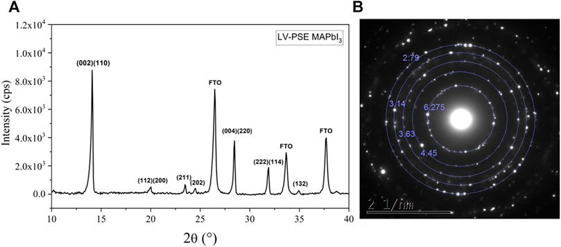
FIGURE 1. (A) XRD diffraction pattern collected on LV-PSE deposited MAPbI3 film on FTO/TiO2 substrate. (B) Electron diffraction pattern collected over a 3 µm2 area by TEM technique on LV-PSE technique on Cu carbon-coated grid directly attached on the glass substrate.
The I4/mcm crystallographic structure of the MAPbI3 film is also confirmed by the electron diffraction analyses performed by TEM, as shown in Figure 1B. In particular, the inner spots corresponding to 6.27 Å are a diagnostic feature of the phase. In the diffraction pattern, there are no features from PbI2, denoting the complete conversion of the PbI2 layer into MAPbI3 by the presented technique. The absence of any amorphous phase in the film is confirmed by the lack of large and diffuse rings in the diffraction pattern. This is a paramount result considering that no post-thermal treatment was performed on the sample after the second deposition step.
The morphology of the as-deposited films was investigated by SEM. Figures 2A,B show the top view of the MAPbI3 films and the cross-sectional images of the complete devices, respectively. As shown in Figure 2A, the MAPbI3 film morphology is very different from the FTO/TiO2 one (Supplementary Figure S2) and is composed of large grains with a size of ∼500 nm and small grains of a size between 100 and 200 nm. The film was highly compact with very well-defined grain boundaries and without pinholes. On the contrary, the FTO/TiO2 morphology is composed of grains with similar dimensions with respect to the MAPbI3 film. However, as can be seen from Supplementary Figure S2A, they have a cuspidal shape with some empty spaces between the grains, while the MAPbI3 ones are well faceted without any empty space between the grains. This might be a consequence of the total conversion of PbI2 into MAPbI3, and such a good quality of the film is also in agreement with the XRD data. In Figure 2B, the cross-sectional SEM image of the complete device confirms that the film is compact, the thickness of the film varies in the range of ∼160–220 nm, and the layer follows the profile of the FTO/TiO2 underlayer, thus creating a good coverage without any break or gap between the perovskite film and the TiO2 surface. The MAPbI3 film is pretty flat on top and has a planarizing effect, so the variation in the film thickness is caused by the roughness of the FTO/TiO2 underlayer.
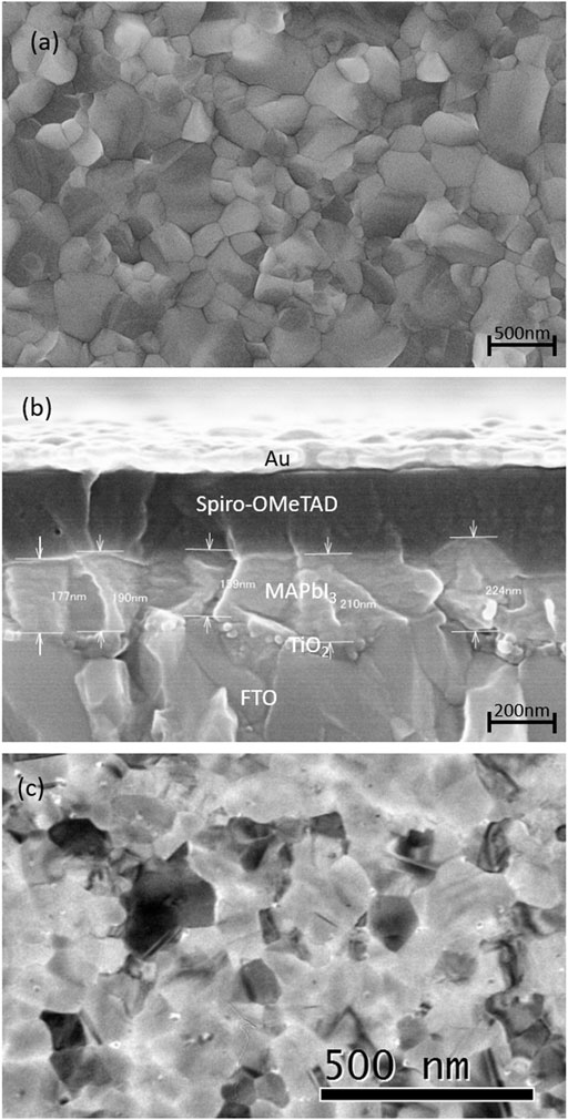
FIGURE 2. (A) SEM top view of the LV-PSE deposited MAPbI3 showing the morphology and the compactness of the film; (B) SEM cross-section of the complete device prepared with the LV-PSE MAPbI3 as the active layer. The thickness varies from 150 to 225 nm. (C) TEM images of LV-PSE deposited MAPbI3 on Cu carbon-coated grid.
The TEM image of the LV-PSE MAPbI3 (Figure 2C) shows a compact layer with some grains that are ∼200 nm large. The difference in grain size with respect to the SEM image is the consequence of the different substrates (Cu carbon-coated grid) used but attests to the quality of the LV-PSE process as it is able to deposit a good quality film on different substrates. It is also worth noting that no amorphous phase is detectable from the TEM analyses, confirming the high crystallographic quality of the films obtained from LV-PSE. The small dark spots are related to the presence of some little metallic Pb precipitates as a result of the prolonged interaction between the electron beam of TEM and the sample, as previously reported in the literature (Alberti et al., 2019b). As these precipitates are not created during a typical degradation of MAPbI3 in the air, they cannot be correlated to the device performance and efficiency.
We have performed a post-thermal treatment to investigate the possibility of increasing the crystal quality of the deposited film. We have performed the annealing in situ at the XRD equipment at 90 and 105°C in dry nitrogen ambient for 1 h and checked the lattice structure (Supplementary Figure S1). After the annealing at 90°C, no changes in the peak intensities for PbI2 (12.76°) and MAPbI3 (14.04°) were detected. After the annealing at 105°C for 1 h, a higher intensity of the peak at 12.67° related to the formation of the PbI2 phase was detected, suggesting that degradation has occurred. As the MAPbI3 film quality looked good in terms of morphology and crystallinity, we prepared devices in an n-i-p architecture using FTO/TiO2/MAPbI3/Spiro-OMeTAD/Au layout to check the photovoltaic performance. In Figure 3, the I-V scan obtained on the best device is presented. The J-V curves displayed large hysteresis between the forward and reverse scan, and the maximum efficiency was 6.30% in the reverse scan (Table 1) which is unexpectedly low if compared with the film prepared by LV-PSE used in a different architecture (Smecca et al., 2021) and the films prepared by solution process using the same architecture (Jena et al., 2020) where efficiency of ∼17% was reached. This led us to doubt the interface quality instead of the bulk of the film. Based on Figure 2B, we can argue that, unlike the case observed by Cojocaru et al. (2018), we did not find any gap between the perovskite TiO2 films, and the layers are well connected; hence, we believed that only such macro defects might not be the reason for lower performance. Shallcross et al. (2019) have suggested that the TiO2 surface defects lead to the formation of a sub-stoichiometric interface layer that has a huge impact on the composition and energy of the co-evaporated MAPbI3 film. It is also well known that the use of organic ETL reduces the hysteresis phenomena, even in the case of evaporated MAPbI3 film, as observed in our previous work (Smecca et al., 2021) and reported by others in the literature (Levine et al., 2016; Zarazua et al., 2016; Cojocaru et al., 2018; Zhong et al., 2020). Therefore, in our case, it is more likely that the defects on the TiO2 surface, which were not treated, coupled with intrinsic ionic mobility in the perovskite, creates a built-in field that leads to inefficient carrier collection resulting in low efficiency and large hysteresis (Patel et al., 2017; Kerner and Rand, 2017). Although there is still room for further improvement, the obtained results demonstrate that the combination of low-vacuum and proximity configuration is viable to grow perovskite layers applied in solar devices. The results are also encouraging due to the reduced thickness of the perovskite layer grown by LV-PSE (190 nm on average).
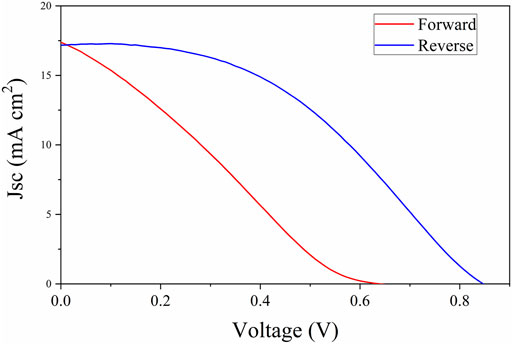
FIGURE 3. I–V characteristic of the complete device with the FTO/TiO2/MAPbI3/Spiro-OMeTAD/Au architecture.
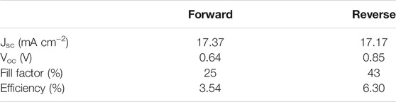
TABLE 1. I-V characteristics as Jsc, Voc, FF, and efficiency calculated from the electrical characterization of the complete device FTO/TiO2/MAPbI3/Spiro-OMeTAD/Au architecture.
To investigate the stability of the MAPbI3 layer, thermal stress tests were applied during in situ spectroscopic ellipsometric analysis. Starting from the as-deposited layer that was probed at a reference temperature of 30°C, the sample was heated up (60, 75, and 90°C) and cooled down to 30°C, as shown in the inset of Figure 4A. This was done to mimic some day/night cycles. The experiment was repeated under humid air and dry nitrogen conditions. Figures 4A,B show the absorption coefficient (a) as a function of the photon energy measured at each temperature along the thermal path. From the curves, the integral values of specific spectral ranges (2.1–3.1 eV and 3.1–4 eV) that fully describe the material behavior (Mannino et al., 2017) were extracted and reported in Figures 4C,D. According to the results, under the stress condition, the MAPbI3 layer shows the beginning of degradation with a 4% loss of absorption capability after annealing in humid air at 90°C. Conversely, in N2 ambient, no sign of degradation is visible even after the 90°C step. The improved stability of MAPbI3 in N2 ambient was extensively studied in previous work (Alberti et al., 2019) that emphasizes how nitrogen acts more than an inert species. Comparing our LV-PSE MAPbI3 films with other previously studied solution-processed film (Mannino et al., 2017; Alberti et al., 2019a), we can argue good stability of the deposited films.
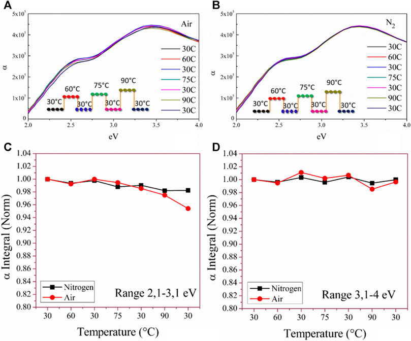
FIGURE 4. Absorption coefficient measured by spectroscopic ellipsometry on MAPbI3 layer deposited on glass at different temperatures in the air (A) and N2 ambient (B); normalized integral of the absorption coefficient in the ranges of 2.1–3 eV (C) and 3.1–4 eV (D) in air and N2 ambient.
Conclusion
We have deposited thin MAPbI3 films on FTO/TiO2 substrate using the new LV-PSE deposition method. The method consists of two steps. In the first one, a PbI2 layer is deposited at ∼4 × 10⁻² mbar low at a distance of ∼2 cm from the source. In the second step, the conversion of the PbI2 film to MAPbI3 occurs by deposition of the organic halide precursor (MAI) at the same pressure and distance. The two steps occur in the same chamber without any vacuum break, thus making the method simple, inexpensive, and industrially appealing. Films that are 190 nm thick on average were characterized in terms of crystal structure, showing the complete conversion of the PbI2 into MAPbI3 without any post-annealing process. Moreover, no sign of residual amorphous phase was found. The film was deposited on FTO/TiO2 substrate without voids or adhesion issues between the TiO2 and the MAPbI3 interfaces. As a proof of concept, a standard n-i-p device was prepared that worked with the best efficiency of 6.30% in reverse scan using just ∼190 nm active layer, showing the potential of the LV-PSE method for future low-cost industrial applications.
Data Availability Statement
The original contributions presented in the study are included in the article/Supplementary Material; further inquiries can be directed to the corresponding author.
Author Contributions
ES was responsible for conceptualization, investigation, data curation, writing the original draft, and revision. AJ was responsible for data curation, investigation, and writing (review and editing). ID contributed to the methodology. SV and SS contributed to the investigation and formal analysis. GM was responsible for the investigation and obtaining the resources. CB contributed to the investigation and data curation. AL was responsible for the methodology and the review and editing process. TM was responsible for obtaining the resources, funding acquisition, and review and editing process. AA contributed to the conceptualization, supervision, obtaining the resources, investigation, data curation, funding acquisition, review and editing process.
Funding
The project was partially supported by the bilateral project on Perovskite Solar Cells (CUP B56C18001070005), co-founded by CNR (Italy) and JSPS (Japan).
Conflict of Interest
The authors declare that the research was conducted in the absence of any commercial or financial relationships that could be construed as a potential conflict of interest.
Publisher’s Note
All claims expressed in this article are solely those of the authors and do not necessarily represent those of their affiliated organizations, or those of the publisher, the editors and the reviewers. Any product that may be evaluated in this article, or claim that may be made by its manufacturer, is not guaranteed or endorsed by the publisher.
Supplementary Material
The Supplementary Material for this article can be found online at: https://www.frontiersin.org/articles/10.3389/felec.2021.726171/full#supplementary-material
References
Alberti, A., Deretzis, I., Mannino, G., Smecca, E., Giannazzo, F., Listorti, A., et al. (2019a). Nitrogen Soaking Promotes Lattice Recovery in Polycrystalline Hybrid Perovskites. Adv. Energ. Mater. 9, 1803450. doi:10.1002/aenm.201803450
Alberti, A., Bongiorno, C., Smecca, E., Deretzis, I., La Magna, A., and Spinella, C. (2019b). Pb Clustering and PbI2 Nanofragmentation during Methylammonium lead Iodide Perovskite Degradation. Nat. Commun. 10, 2196. doi:10.1038/s41467-019-09909-0
Burschka, J., Pellet, N., Moon, S.-J., Humphry-Baker, R., Gao, P., Nazeeruddin, M. K., et al. (2013). Sequential Deposition as a Route to High-Performance Perovskite-Sensitized Solar Cells. Nature 499, 316–319. doi:10.1038/nature12340
Chen, Q., Zhou, H., Hong, Z., Luo, S., Duan, H.-S., Wang, H.-H., et al. (2014). Planar Heterojunction Perovskite Solar Cells via Vapor-Assisted Solution Process. J. Am. Chem. Soc. 136, 622–625. doi:10.1021/ja411509g
Cojocaru, L., Wienands, K., Kim, T. W., Uchida, S., Bett, A. J., Rafizadeh, S., et al. (2018). Detailed Investigation of Evaporated Perovskite Absorbers with High Crystal Quality on Different Substrates. ACS Appl. Mater. Inter. 10, 26293–26302. doi:10.1021/acsami.8b07999
Deretzis, I., Smecca, E., Mannino, G., La Magna, A., Miyasaka, T., and Alberti, A. (2018). Stability and Degradation in Hybrid Perovskites: Is the Glass Half-Empty or Half-Full? J. Phys. Chem. Lett. 9, 3000–3007. doi:10.1021/acs.jpclett.8b00120
Eperon, G. E., Burlakov, V. M., Docampo, P., Goriely, A., and Snaith, H. J. (2014). Morphological Control for High Performance, Solution-Processed Planar Heterojunction Perovskite Solar Cells. Adv. Funct. Mater. 24, 151–157. doi:10.1002/adfm.201302090
Guo, Q., Li, C., Qiao, W., Ma, S., Wang, F., Zhang, B., et al. (2016). The Growth of a CH3NH3PbI3 Thin Film Using Simplified Close Space Sublimation for Efficient and Large Dimensional Perovskite Solar Cells. Energy Environ. Sci. 9, 1486–1494. doi:10.1039/c5ee03620h
Im, J.-H., Jang, I.-H., Pellet, N., Grätzel, M., and Park, N.-G. (2014). Growth of CH3NH3PbI3 Cuboids with Controlled Size for High-Efficiency Perovskite Solar Cells. Nat. Nanotech 9, 927–932. doi:10.1038/nnano.2014.181
IRENA (2021). International Renewable Energy Agency. Available at: https://www.irena.org/. (Accessed June 10, 2021).
Jena, A. K., Ishii, A., Guo, Z., Kamarudin, M. A., Hayase, S., and Miyasaka, T. (2020). Cesium Acetate-Induced Interfacial Compositional Change and Graded Band Level in MAPbI3 Perovskite Solar Cells. ACS Appl. Mater. Inter. 12 (30), 33631–33637. doi:10.1021/acsami.0c06315
Jeon, N. J., Noh, J. H., Kim, Y. C., Yang, W. S., Ryu, S., and Seok, S. I. (2014). Solvent Engineering for High-Performance Inorganic-Organic Hybrid Perovskite Solar Cells. Nat. Mater 13, 897–903. doi:10.1038/nmat4014
Kerner, R. A., and Rand, B. P. (2017). Linking Chemistry at the TiO2/CH3NH3PbI3 Interface to Current-Voltage Hysteresis. J. Phys. Chem. Lett. 8, 2298–2303. doi:10.1021/acs.jpclett.7b00712
Kojima, A., Teshima, K., Shirai, Y., and Miyasaka, T. (2009). Organometal Halide Perovskites as Visible-Light Sensitizers for Photovoltaic Cells. J. Am. Chem. Soc. 131, 6050–6051. doi:10.1021/ja809598r
Levine, I., Nayak, P. K., Wang, J. T.-W., Sakai, N., Van Reenen, S., Brenner, T. M., et al. (2016). Interface-Dependent Ion Migration/Accumulation Controls Hysteresis in MAPbI3 Solar Cells. J. Phys. Chem. C 120, 16399–16411. doi:10.1021/acs.jpcc.6b04233
Leyden, M. R., Ono, L. K., Raga, S. R., Kato, Y., Wang, S., and Qi, Y. (2014). High Performance Perovskite Solar Cells by Hybrid Chemical Vapor Deposition. J. Mater. Chem. A. 2, 18742–18745. doi:10.1039/c4ta04385e
Li, J., Wang, H., Chin, X. Y., Dewi, H. A., Vergeer, K., Goh, J., et al. (2020). Highly Efficient Thermally Co-evaporated Perovskite Solar Cells and Mini-Modules. Joule 4, 1035–1053. doi:10.1016/j.joule.2020.03.005
Liu, M., Johnston, M. B., and Snaith, H. J. (2013). Efficient Planar Heterojunction Perovskite Solar Cells by Vapour Deposition. Nature 501, 395–398. doi:10.1038/nature12509
Luo, P., Liu, Z., Xia, W., Yuan, C., Cheng, J., and Lu, Y. (2015). Uniform, Stable, and Efficient Planar-Heterojunction Perovskite Solar Cells by Facile Low-Pressure Chemical Vapor Deposition under Fully Open-Air Conditions. ACS Appl. Mater. Inter. 7, 2708–2714. doi:10.1021/am5077588
Mannino, G., Alberti, A., Deretzis, I., Smecca, E., Sanzaro, S., Numata, Y., et al. (2017). First Evidence of CH3NH3PbI3 Optical Constants Improvement in a N2 Environment in the Range 40-80 °C. J. Phys. Chem. C 121, 7703–7710. doi:10.1021/acs.jpcc.7b00764
National Renewable Energy Laboratory (NREL) (2021). Best Research-Cell Efficiency Chart. Available at: https://www.nrel.gov/pv/cell-efficiency.html. (Accessed June 10, 2021).
Patel, J. B., Wong-Leung, J., Van Reenen, S., Sakai, N., Tse Wei Wang, J., Parrott, E. S., et al. (2017). Influence of Interface Morphology on Hysteresis in Vapor-Deposited Perovskite Solar Cells. Adv. Electron. Mater. 3, 1600470. doi:10.1002/aelm.201600470
Pérez-del-Rey, D., Boix, P. P., Sessolo, M., Hadipour, A., and Bolink, H. J. (2018). Interfacial Modification for High-Efficiency Vapor-Phase-Deposited Perovskite Solar Cells Based on a Metal Oxide Buffer Layer. J. Phys. Chem. Lett. 9, 1041–1046. doi:10.1021/acs.jpclett.7b03361
Shallcross, R. C., Olthof, S., Meerholz, K., and Armstrong, N. R. (2019). Impact of Titanium Dioxide Surface Defects on the Interfacial Composition and Energetics of Evaporated Perovskite Active Layers. ACS Appl. Mater. Inter. 11, 32500–32508. doi:10.1021/acsami.9b09935
Smecca, E., Numata, Y., Deretzis, I., Pellegrino, G., Boninelli, S., Miyasaka, T., et al. (2016). Stability of Solution-Processed MAPbI3 and FAPbI3 Layers. Phys. Chem. Chem. Phys. 18, 13413–13422. doi:10.1039/c6cp00721j
Smecca, E., Valenzano, V., Valastro, S., Deretzis, I., Mannino, G., Malandrino, G., et al. (2021). Two-step MAPbI3 Deposition by Low-Vacuum Proximity-Space-Effusion for High-Efficiency Inverted Semitransparent Perovskite Solar Cells. J. Mater. Chem. A. 9, 16456–16469. doi:10.1039/d1ta02535j
Zarazua, I., Han, G., Boix, P. P., Mhaisalkar, S., Fabregat-Santiago, F., Mora-Seró, I., et al. (2016). Surface Recombination and Collection Efficiency in Perovskite Solar Cells from Impedance Analysis. J. Phys. Chem. Lett. 7, 5105–5113. doi:10.1021/acs.jpclett.6b02193
Keywords: LV-PSE, physical deposition, MAPbI3, TiO2, low temperature
Citation: Smecca E, Jena AK, Deretzis I, Valastro S, Sanzaro S, Mannino G, Bongiorno C, La Magna A, Miyasaka T and Alberti A (2021) MAPbI3 Deposition by LV-PSE on TiO2 for Photovoltaic Application. Front. Electron. 2:726171. doi: 10.3389/felec.2021.726171
Received: 16 June 2021; Accepted: 06 September 2021;
Published: 24 September 2021.
Edited by:
Aurora Rizzo, Italian National Research Council, ItalyReviewed by:
Thomas Stergiopoulos, Aristotle University of Thessaloniki, GreeceRoberto Mosca, Italian National Research Council, Italy
Copyright © 2021 Smecca, Jena, Deretzis, Valastro, Sanzaro, Mannino, Bongiorno, La Magna, Miyasaka and Alberti. This is an open-access article distributed under the terms of the Creative Commons Attribution License (CC BY). The use, distribution or reproduction in other forums is permitted, provided the original author(s) and the copyright owner(s) are credited and that the original publication in this journal is cited, in accordance with accepted academic practice. No use, distribution or reproduction is permitted which does not comply with these terms.
*Correspondence: Alessandra Alberti, YWxlc3NhbmRyYS5hbGJlcnRpQGltbS5jbnIuaXQ=