 Inam Mirza1Alexander V. Bulgakov1Hanna Sopha2,3Sergey V. Starinskiy4,5Hana Turčičová1Ondřej Novák1Jiří Mužík1Martin Smrž1Vladimir A. Volodin5,6Tomáš Mocek1
 Jan M. Macak2,3
 Nadezhda M. Bulgakova1*
- 1HiLASE Centre, Institute of Physics of the Czech Academy of Sciences, Dolní Břežany, Czechia
- 2Center of Materials and Nanotechnologies, Faculty of Chemical Technology, University of Pardubice, Pardubice, Czechia
- 3Central European Institute of Technology, Brno University of Technology, Brno, Czechia
- 4S.S. Kutateladze Institute of Thermophysics SB RAS, Novosibirsk, Russia
- 5Physics Department, Novosibirsk State University, Novosibirsk, Russia
- 6Rzhanov Institute of Semiconductor Physics SB RAS, Novosibirsk, Russia
As-prepared nanostructured semiconductor materials are usually found in an amorphous form, which needs to be converted into a crystalline one for improving electronic properties and achieving enhanced application functionalities. The most utilized method is thermal annealing in a furnace, which however is time- and energy-consuming and not applicable for low-temperature melting substrates. An alternative is laser annealing, which can be carried out in a relatively short time and, additionally, offers the possibility of annealing localized areas. However, laser-annealed nanostructures are often distorted by melting, while preserving the as-prepared morphology is essential for practical applications. In this work, we analyze conditions of non-thermal ultrafast laser annealing of two kinds of nanostructures: anodic TiO2 nanotube layers and Ge/Si multilayer stacks. For both cases, regimes of crystallization have been found, which yield in preserving the initial nanomaterial morphologies without any melting signs. On these examples, ultrafast non-thermal mechanisms of structural material transformation are discussed, which can provide new opportunities for conversion of amorphous semiconductor nanomaterials into a desired crystalline form that is of high demand for existing and emerging technologies.
1 Introduction
Nowadays semiconductor nanomaterials (SNM) such as thin films, nanowires, nanotubular structures and their layers have become building blocks in many industrial applications that also stimulates extensive research of novel SNMs, their properties and the ways to enhance functionalities of such materials (Wang et al., 2014; Benelmekki and Erbe, 2019; Mullen and Morris, 2021; Xu et al., 2021). The application areas for the SNMs are very wide and range from micro-/nanoelectronics (Mullen and Morris, 2021), photonics (David et al., 2021), solar energy harvesting (Zhang et al., 2022; Toolan et al., 2023), sensing (Feng et al., 2023), catalysis (Feliczak-Guzik, 2023; Güell et al., 2023), and biomedical applications including drug delivery and diagnostics of therapy of diseases such as cardiovascular problems and malignant tumors (Walkey et al., 2009; Oleshchenko et al., 2020; Yuan et al., 2022; Flimelova et al., 2023). Many of such materials in the as-prepared form are amorphous. Although amorphous SNMs are also widely used in various fields (Ng et al., 2019; Motola et al., 2020; Wang et al., 2021), their crystalline forms often exhibit physical and chemical properties much more suitable for many specific applications (Yu et al., 2017; Kryshtal et al., 2022). Thus, there are needs in the techniques which enable reliable and reproducible crystallization of semiconductor nanomaterials, often locally and selectively, to fabricate high-quality products. There are many means to convert amorphous SNMs into a crystalline phase such as thermal annealing, chemical methods including metal-assisted crystallization (Zamchiy et al., 2021; Kryshtal et al., 2022), laser and electron beam irradiation (Jenčič et al., 1995; Egan et al., 2019), plasma (Benčina et al., 2019) or microwave (Aquino et al., 2016) annealing. All these methods have specifics in applications to different types of nanomaterials and often are not suitable for particular materials.
Among the listed methods, laser annealing has great potential (Vainos, 2012; Aktas and Peacock, 2021), given a wide variety of laser sources with different parameters in terms of power, laser wavelength, pulse duration, and peak intensity. Important features of laser annealing are that it can allow a localized conversion of amorphous to a crystalline form without affecting the underlying substrates (Sopha et al., 2020) and/or highly selective crystallization of components in multimaterial nanostructures (Volodin et al., 2023) at properly chosen irradiation parameters. In both these examples, ultrashort-pulse lasers were employed that may look contra-intuitive and incompatible with thermal annealing mechanisms. Indeed, the majority of annealing techniques are based on a prolonged exposure of the material to an energy source for inducing structural transformation. Here we investigate and discuss the ultrashort-laser-pulse crystallization of amorphous TiO2 nanotubes to the anatase phase without any melting signs and the absence of intermixture of silicon and germanium upon ultrashort-pulse laser annealing of amorphous Ge/Si multilayer stacks. These two structured materials in a crystalline form have a very large potential for many applications. Highly ordered, anodic TiO2 nanotube layers attract considerable attention in the fields of solar energy harvesting, photocatalysis, and sensing (Sopha et al., 2020) while Ge/Si multilayer stacks are of high demand in photovoltaics and micro/nano electronics and are suitable for flexible electronic devices (Ding et al., 2021; Volodin et al., 2023). To understand the mechanisms of laser-induced transformations achieved in this work, we involve concepts of non-equilibrium ultrafast processes such as explosive crystallization induced by laser generated stress waves and ultrafast laser melting. The requirements for the laser parameters to induce crystallization without damaging material morphology are analyzed.
2 Laser annealing of amorphous TiO2 nanotube layers into anatase
Nanostructured TiO2 materials are widely used in various applications, such as nanocrystalline solar cell technologies, photocatalysis, purification of water from hazardous industrial byproducts, in nanomedicine as components for imaging and therapeutics, and as antibacterial agents (Waghmode et al., 2019). This is due to their excellent photocatalytic properties, enhanced absorption in the UV spectral range, high thermal and chemical stability, and biocompatibility. Among crystalline polymorphs of TiO2 (rutile, anatase, and brookite), anatase has the best photocatalytic activity (Hoffmann et al., 1995; Rajeshwar, 1995; Luttrell et al., 2014; Zhang et al., 2014). In the past, different chemical and physical techniques have been applied to synthesize and crystallize TiO2 nanomaterial (nanopowder, deposited nanostructured films, nanotubular layers) to explore their photocatalytic properties. The TiO2 nanotube (TNT) layers are one of the most promising structures for catalytic applications (Macak et al., 2007; Lamberti et al., 2015; Sopha et al., 2018) due to their large surface area and a relatively simple technique for their fabrication through the controlled and optimized anodization process allowing preparation of the layers up to several hundreds of micrometers in thickness (Macák et al., 2005; Sopha et al., 2018). Additionally, such TNT layers possess excellent sensing properties (Varghese et al., 2003). They demonstrate the best catalytic and sensing activities, when their initial amorphous form is transformed into the anatase phase (Macak et al., 2007). As mentioned above, different methods are known to modify as-prepared amorphous TNT layers to a crystalline phase (see an overview by Sopha et al., 2020). Here we focus on laser-induced annealing, which can enable highly localized and selective annealing without affecting the underlying substrate (Sopha et al., 2020). However, laser annealing is not a straightforward process, and the laser parameters require to be carefully optimized for obtaining a desired phase with the best functional characteristics (Wawrzyniak et al., 2020a; Wawrzyniak et al., 2020b; Sopha et al., 2020; Siuzdak et al., 2023). In our study, several lasers with different irradiation parameters have been used in order to learn the modification mechanisms. Among them, only one laser type enabled to modify the amorphous TNT layers into the anatase phase while preserving the initial nanotube morphology. We analyze the parameters of the applied lasers and discuss the underlying physics of phase transformation.
2.1 TNT layer preparation
The TNT layers of thicknesses of ∼1 μm and ∼20 µm with the nanotube diameter of ∼80 nm and ∼110 nm respectively were prepared by electrochemical anodization of Ti foils as described in the previous papers (Das et al., 2016; Zazpe et al., 2016). In brief, Ti foils (0.127-mm thick, Sigma-Aldrich, 99.7% purity) were degreased by sonication in isopropanol and acetone and dried in air. Afterwards, the Ti foils were anodized at room temperature in an electrochemical cell using a 2-electrode configuration with the Ti foil serving as anode and a Pt foil as a cathode. A high-voltage potentiostat (PGU-200, Elektroniklabor GmbH) was employed as a voltage source. ∼1 µm thick TNT layers were produced in a glycerol-based electrolyte containing 50 vol% H2O and 270 mM NH4F (Sigma-Aldrich, reagent grade) at 20 V for 100 min (Das et al., 2016). ∼20 µm thick TNT layers were produced in an ethylene glycol-based electrolyte containing 1.5 vol% H2O and 170 mM NH4F at 60 V for 4 h (Zazpe et al., 2016). The anodized area of each foil was 1 cm2. After anodization, the TNT layers were rinsed, sonicated in isopropanol, and dried in air.
The morphology of the TNT layers was characterized by a field-emission Scanning Electron Microscope (FE-SEM JEOL JSM 7500F) and by a High-Resolution Transmission Electron Microscope (FEI Titan Themis 60–300) operated at 300 keV and equipped with a Cs (spherical aberration) image corrector. Raman spectra were recorded by LabRAM HR (Horiba Jobin Yvon) and acquired in a continuous scanning mode under a laser excitation wavelength of 532 nm. The composition of the TNT layers was monitored by X-ray Photoelectron Spectroscopy (XPS) (ESCA2SR, Scienta-Omicron) using a monochromatic Al Ka (1,486.7 eV) X-ray source. A typical image of an as-prepared ∼20 µm thick TNT layer used in the laser annealing experiments, a magnified view of the nanotubes from the top of the layer, and its cross-sectional view are shown in Figure 1.
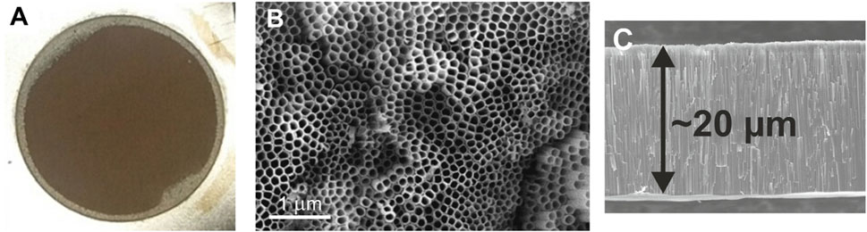
FIGURE 1. (A) An optical image of the as deposited sample 1 cm in diameter with the TiO2 NT layer of ∼20 μm thickness. (B) A scanning electron micrograph of the as-deposited TNT layer with the nanotube diameter of ∼110 nm. (C) A cross-sectional image of an as-deposited ∼20-µm-thick TNT layer.
2.2 Lasers for annealing
The band gap of the main crystalline phases of TiO2 is somewhat larger than 3 eV (Scanlon et al., 2013). Hence, for efficient absorption of laser light with a nanosecond pulse duration, a UV spectral range is appropriate (Wawrzyniak et al., 2020a; Wawrzyniak et al., 2020b; Siuzdak et al., 2023). However, the absorption depth for UV light is rather short, of the order of few dozens of nanometers. To evaluate the absorption depth, we have applied the Maxwell-Garnett effective medium framework (Heavens, 1960). The effective medium theory allows evaluating the optical properties of composite and porous materials via taking into account the dielectric function of each component. The Maxwell-Garnet expression for the TiO2 nanotubes under air surrounding can be written as
where
The results of calculations of the absorption depth and the reflection coefficient based on the above formulas are shown in Figure 2 for a 260 nm wavelength and similar results are obtained for wavelengths of 193 nm (ArF laser) and 355 nm (Siuzdak et al., 2023). For ∼40% volume fraction of TiO2 in TNT layers, absorption is mostly localized in a ∼100-nm top layer. Hence, in the UV spectral range, light absorption takes place on the tops of TNT layers, leading to local heating and melting, while the heat extraction along nanotubes is relatively slow. Indeed, from the heat flux equation, one can easily extract an evaluating expression
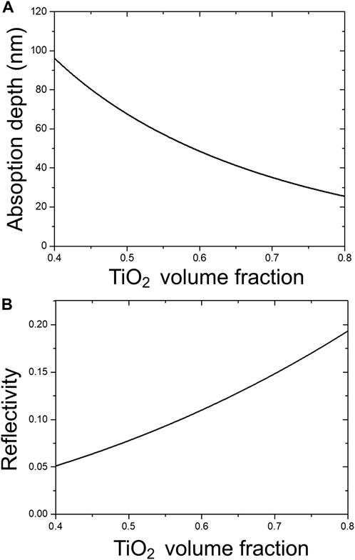
FIGURE 2. The TNT layer absorption depth (A) and the reflectivity of the array layers (B) evaluated using the Maxwell-Garnett effective medium theory as a function of TiO2 volume fraction.
To explore the possibilities of laser annealing of the TNT layers with minimal damage to their morphology, we have used different lasers, which are outlined in Table 1 and their applications are analyzed in the next sections.
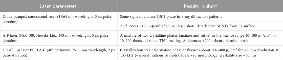
TABLE 1. Specifications of the applied lasers and a short summary of TNT annealing results.
2.2.1 IR diode ns laser
As the absorption in the UV spectral range takes place on the very top of the TNT layers, a part of the experiments was performed with IR pulses using a hand-made diode-pumped nanosecond laser (1,064 nm wavelength; 3 ns pulse duration; 150 kHz repetition rate). The spot size on the surface was ∼200 µm and the fluence was varied in the range of 50–200 mJ/cm2. The samples were scanned at the velocity of 0.7 m/sec. It was evaluated that app. 40 shots were coupling each point upon scanning.
After irradiation, the color of the layers became slightly darker as compared to the original color shown in Figure 1A but still yellowish. The samples remain essentially amorphous (Figure 3). However, some signs of an anatase peak of (101) direction between 2θ of 25° and 30° can be seen. This may indicate a partial, yet very minor crystallization. With increasing laser fluence, the TNT layer becomes darker while delamination from the Ti underlying substrate is found. Thus, as the TiO2 is transparent for IR irradiation, the titanium substrate absorbs the laser light efficiently [absorption depth ∼21 nm (Palik, 1998)]. As a result, the TNT layers are heated from the bottom and can be detached from the substrate due to thermal stress (Meshcheryakov and Bulgakova, 2006). Hence, the IR laser annealing of TiO2 into its crystalline forms is not appropriate.
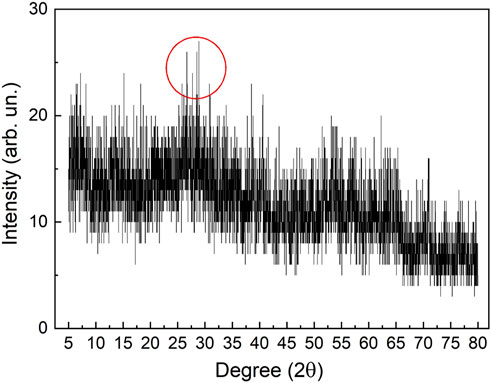
FIGURE 3. X-ray diffraction pattern of a TNT layer annealed by the nanosecond laser (1,064 nm wavelength; 3 ns pulse duration). The TiO2 remains substantially amorphous. Some signs of the anatase peak at 2θ between 25° and 30° (outlined by the red circle) may indicate a partial, yet very minor crystallization.
2.2.2 ArF nanosecond laser
In the next set of experiments, the TNT layers were irradiated by an ArF excimer laser beam (193 nm wavelength, 5 ns pulse duration). Two TNT layers were irradiated, with 20 μm and 1 µm thicknesses. For both layers, several spots at different irradiation conditions have been produced. The results are shown in Figure 4 for the 20-µm thick layer (results for the 1-µm layer are similar and not shown here). The spots outlined by green circles refer to the ArF laser irradiation while the spots in red circles were produced by the PERLA-C laser (see discussion below). The irradiation conditions for the spots in Figure 4 are summarized in Table 2.
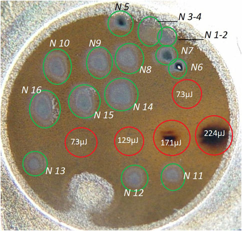
FIGURE 4. The TNT layer irradiated by spots with different irradiation conditions specified in Table 2. The spots outlined by green circles correspond to ArF laser irradiation. The spots outlined by red circles were produced by irradiation with the PERLA-C laser.
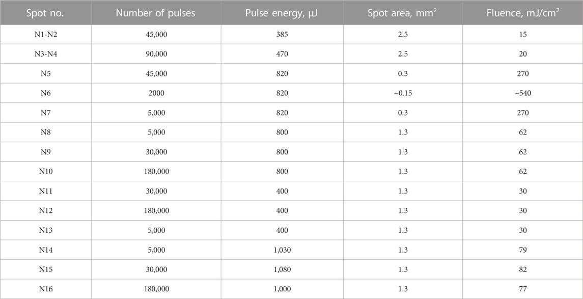
TABLE 2. The irradiation conditions for each spot in Figure 4 produced by ArF laser.
The Raman spectra show that all laser-modified areas represent various combinations of rutile and anatase phases depending on the laser fluence and pulse number. In Figure 5A, typical spectra are shown for spots N14-N16. The reference spectra for rutile and anatase are given in Figure 5B. The higher the laser fluence, the higher is the quality of the spectrum (with low noise). However, as expected, the tops of nanotubes are considerably distorted by melting (inset in Figure 5A for the spot N14), similar to that demonstrated for 266-nm wavelength irradiation (Wawrzyniak et al., 2020a). Furthermore, the TNT layer experiences considerable ablation at enhanced laser fluences (N5–N7).
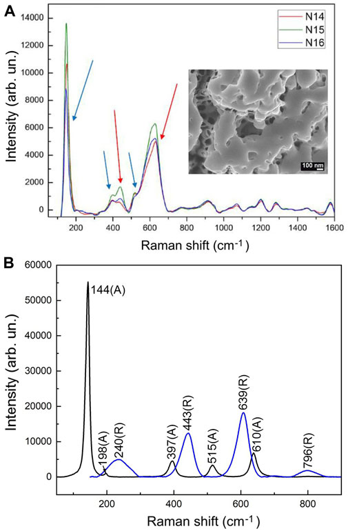
FIGURE 5. (A) Raman spectra obtained for the spots N14–N16 in Figure 4 irradiation with ArF laser. Higher laser intensity produces a higher quality spectrum with lower noise. Blue and red arrows point to the peaks of anatase and rutile respectively. In the inset, an SEM image of a fragment of the N14 spot is shown, demonstrating that the top layer of the TNT layer experienced melting. (B) Reference spectra of rutile and anatase phases. The labels (A) and (R) refer to anatase and rutile respectively.
Based on the results with nanosecond lasers, attempts were made to anneal the TNT arrays with ultrashort laser pulses at a UV wavelength, where the physics of material transformation changes significantly toward the creation of high stresses (stress confinement regimes) (Karim et al., 2016). It could be expected that, under high stresses, a metastable amorphous semiconductor can be converted into a more stable crystalline phase (Volodin et al., 2023).
2.2.3 Fourth harmonic of the HiLASE PERLA-C laser
The picosecond diode-pumped thin-disk laser source PERLA-C has been developed at the HiLASE centre (fundamental laser wavelength of 1,030 nm, 2 ps pulse duration) (Novák et al., 2016; Smrz et al., 2019; Turcicova et al., 2019). For annealing, the fourth harmonics of the laser (257.5 nm) was used to ensure single photon absorption of laser light by the TNT layers. The irradiation was performed at a 89 kHz repetition rate with 5 W maximum average power and ∼56 µJ maximum pulse energy. The laser pulse energy was controlled by a combination of a half-wave plate and a thin film polarizer. The high available pulse energy of the HiLASE laser source enabled to use the direct laser output beam without focusing optics to irradiate the samples.
The measured fluence distribution on the sample surface can be approximated by an elliptical Gaussian beam with 1/e2 diameters of 2.9 mm and 2.5 mm along the x and y directions respectively. In the present experiments, the peak laser fluence was varied in the range from 0.25 to 1.5 mJ/cm2. Scanning of the TNT layers to anneal them over the whole area was performed in a bidirectional fashion (right-left-right). Figures 6A–D present SEM images of a TNT layer at different magnifications, which was scanned at a speed of 0.25 mm/s along x direction with a 0.5 mm step along y direction at an optimal laser fluence of 1 mJ/cm2 while the TNT layer was converted from the amorphous form to anatase without signs of melting. No rutile signatures were observed in the Raman spectra (Figure 7). The time to anneal the whole sample with a surface area of 1 cm2 is ∼14 min. The number of laser shots per site along the scanline can be evaluated as 106. A video of laser annealing is presented in Supplementary Material.
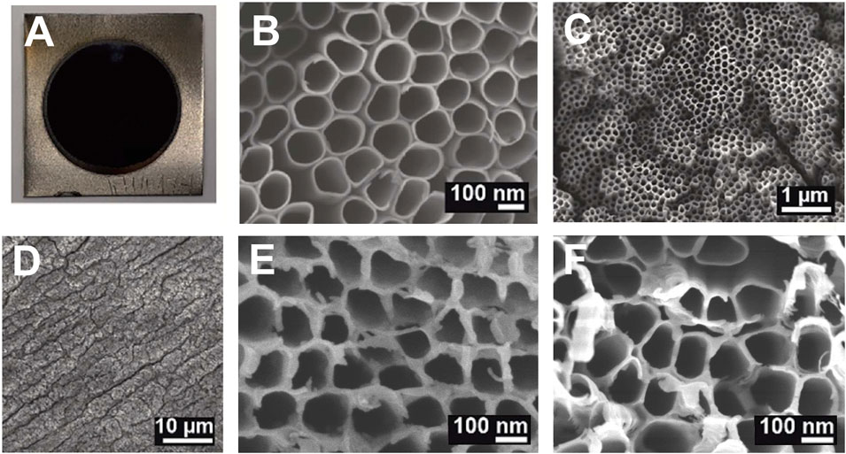
FIGURE 6. The TNT layers annealed with the HiLASE PERLA-C laser. (A) An optical image of the laser-annealed TNT layer at the optimal conditions (peak fuence of ∼1 mJ/cm2, ∼106 pulses per sight). (B)–(D) Magnified views (SEM images) of the sample shown in (A). No signs of melting are visible. (E) 0.83 mJ/cm2, 107 laser shots per site; (F) 0.81 mJ/cm2, 2×10⁷ shots. At higher irradiation doses, the TNT tops experience melting (E) and ablation (F). However, the nanotubes remain open with rather minor distortion (compare with image in the inset of Figure 5).
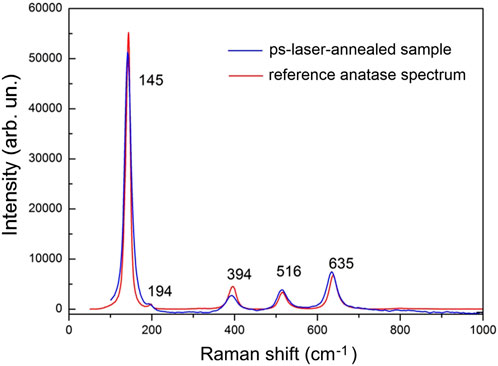
FIGURE 7. Raman spectra typical for the ultrashort laser annealed samples as presented in Figure 6.
The optimal irradiation conditions were found by irradiation of fixed spots on the sample (without scanning) with different laser fluences and different numbers of laser shots per spot (irradiation time). Some of such spots outlined by red circles are shown in Figure 4. The color of such spots is dark brown, almost black, which is very different from the ArF laser annealed spots. This dark color can be a sign of a high concentration of Ti3+ species.
At low laser fluences or low number of shots per site, the amorphous phase was largely preserved. By exceeding the irradiation dose per spot above the revealed optimal conditions (about 106 laser shots at ∼1 mJ/cm2), melting and ablation were found on the top of the TNT layers, although with efficient converting the amorphous phase into anatase. SEM images (E) and (F) in Figure 6 correspond to higher doses than the optimal one at the same laser fluence (107 and 2×10⁷ shots respectively). It is evident that the TNTs in both spots were ablated on the top. However, while the TNTs in (E) exhibit slightly molten and disintegrated nanotube walls, the nanotube walls in (F) do not seem to be molten although the irradiation dose obtained is almost twice higher. Instead, some deposits can be found on top of the TNTs in (F). We anticipate that, in the case of (F) due to heat accumulation on the top of nanotubes upon irradiation, the heat affected area is massively ablated with uncovering unmolten nanotubes. Indeed, some solidified droplets are seen in (F) which could probably redeposit upon ablation in open air. At a lower irradiation dose (E), the edgings of the nanotubes experienced melting. However, as compared to nanosecond UV laser annealing, the ultrashort-laser-annealed nanotube layers remain open on the top with the large surface area (compare with the SEM image in Figure 5) and for some applications such as catalysis can still be useful, provided that the TNTs represent pure anatase structures. In the next section, we discuss mechanisms that can be responsible for the amorphous-to-anatase phase transition.
2.3 Pressure-induced solid phase crystallization of TNT layers induced by ps UV laser
We anticipate that, at optimal conditions of ultrashort laser annealing, we observe an effect of the pressure-induced solid-phase crystallization, often called explosive crystallization. The pressure-induced crystallization represents a transition from the low density amorphous to a higher density (pressurized) amorphous phase, followed by crystallization (Pandey et al., 2011). Ultrashort laser heating of a top layer of a sample may yield a strong unloading stress/shock wave propagating toward the sample depth (Zhigilei et al., 2009; Karim et al., 2016), which can trigger such phase transformation. Let us evaluate the possibility of a shock/compression wave under our irradiation condition in the stress-confinement regime.
The absorbed laser energy at the top of the nanotube can be evaluated as
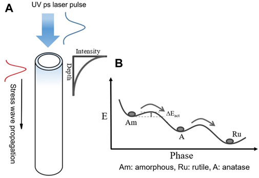
FIGURE 8. (A) Schematics of a stress/shock wave initiation upon ultrashort laser annealing of the TiO2 nanotubes. (B) A sketch for phase transformation from the amorphous state to anatase and rutile.
The activation energy ΔEact for amorphous-to-anatase transformation is 69 kJ/mol, lower than that for anatase-to-rutile transformation (129 kJ/mol), that is in favor of anatase formation at relatively mild stresses (Figure 8B). We also note that, according to Ostwald’s rule (Ostwald, 1897), phase transformation proceeds first not to the most stable phase (rutile in the case of TiO2) but to a less stable polymorph which is closest in energy to the original state (anatase for TiO2 although it is a metastable phase). On the release path of the shock wave, the sequence of observed phase transitions depends on whether the pressure is reduced slowly or rapidly or, in other words, if the new crystalline phase is frozen or can further transform into a more stable phase.
Summarizing, the laser-induced crystallization of the amorphous TNT layers into anatase with the HiLASE PERLA-C laser is a fast and clean process, avoiding oxidation of underlying titanium substrate and enabling to produce a patterned crystallization in localized areas. Such a solid-phase crystallization can be performed by other ultrashort laser systems, provided that the energy of their harmonics in the UV spectral range is sufficient for triggering crystallization. As soon as the absorbed laser energy exceeds the threshold for TiO2 melting, either in a single pulse or upon heat accumulation at multipulse irradiation, the TNTs are melted and can be distorted. However, we found that, at ultrashort laser irradiation, the distortion is considerably lower than for nanosecond laser pulses. In the next sections we will discuss the mechanism of another solid phase crystallization effect upon laser annealing of stacks of amorphous Ge/Si nanolayers.
3 On the possibility and mechanisms of solid-phase crystallization of amorphous Ge nanofilms in a-Ge/a-Si multilayer stacks
Multilayered semiconductors have attracted considerable attention due to their exceptional absorption properties in a wide spectral range from UV to mid-infrared that make them suitable for applications in solar elements, high-performance microelectronic devices, photodetectors, sensors, and portable electronics (Paul, 2004; Wang et al., 2005; Krivyakinet al., 2017; Lee et al., 2019; Pan et al., 2021; Yang et al., 2021). As-deposited multilayered semiconductor films are usually amorphous and, for improving their quality for various applications, crystallization is needed with avoiding intermixing between layers (Kolchin et al., 2020). Recently, we have achieved selective crystallization of amorphous Ge nanolayers in a-Ge/a-Si multilayer stacks (Volodin et al., 2023). The best results were achieved by using femtosecond laser pulses at 1.5-µm wavelength when nanocrystallites were formed in Ge layers while Si remained intact and no signs of intermixing of Ge and Si at interfaces between the layers were observed. We put forward a hypothesis on the possibility of ultrafast solid-solid phase transition and here we assess this conclusion in comparison with the TNT layer crystallization.
3.1 Toward mid-IR selective laser annealing
The samples for laser annealing represented stacks of hydrogenated amorphous germanium (a-Ge) and amorphous silicon (a-Si) alternating nanolayers with thicknesses 15 nm and 40 nm respectively deposited on a Si(100) substrate by Plasma-Enhanced Chemical Vapor Deposition (PECVD) with a-Si as the top layer (Figure 9). The substrate temperature during deposition was 225°C. The precursor was germane (GeH4) or silane (SiH4) diluted with argon, leading to hydrogen being present in the amorphous germanium and silicon alternating nanolayers. Growth conditions are described in more detail in (Volodin et al., 2023).
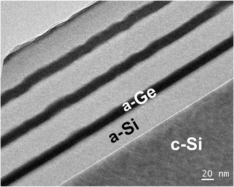
FIGURE 9. Transmission electron microscope image of as-deposited a-Si/a-Ge multilayer stack. Ge layers are dark while Si layers are light grey.
Two laser systems were used to anneal the multilayered samples, a picosecond laser (HiLASE PERLA-B, λ = 1,030 nm, pulse duration 1.4 ps, pulse energy up to 10 mJ) and a femtosecond laser (Astrella, Coherent) in combination with an optical parametric amplifier (TOPAS, Light Conversion). The latter enables tuning the laser wavelength in the range from 1,160 nm to 15 µm. In this work, we will focus on the results obtained at λ = 1,500 nm with a pulse duration of 70 fs and pulse energy up to 0.4 mJ, which provided the best results of annealing, presumably without melting. All the results which will be discussed below were obtained at single-pulse irradiation. More experimental details can be found in (Volodin et al., 2023).
Figure 10 presents Raman spectra of the sample sites annealed by femtosecond pulses at different peak laser fluences. The Raman spectrum of the original sample is also presented, showing that both Si and Ge are purely amorphous (a-Si and a-Ge). The sample modification threshold fluence was measured to be ∼50 mJ/cm2. Starting from this fluence, a peak of crystalline Ge begins to appear in the Raman signal. At a fluence of 64 mJ/cm2, the crystalline Ge peak is distinct while Si does not show any modification and there are no signs of Si-Ge intermixing (red dashed line in Figure 10). The percentage of crystallization (fraction of Ge nanocrystals in the a-Ge matrix) is evaluated as ∼30%. The evaluation is based on the following expression (Hao et al., 2020)
where
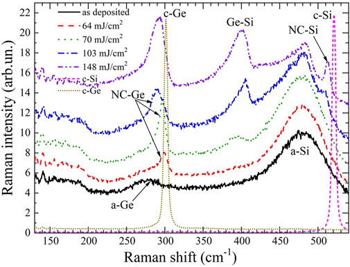
FIGURE 10. Raman spectra of the pulse-laser annealed Si/Ge multilayer stack shown in Figure 9. For reference, the peaks of crystalline silicon and germanium (c-Si and c-Ge respectively) are also added. Annealing was performed at a wavelength of 1.5 µm and pulse duration of ∼70 fs that assumes considerable contribution of non-linear absorption in Ge layers. At low laser fluences slightly above the modification threshold, nano-crystallization of Ge is observed without visible effects of melting (red dashed line). With increasing laser fluence (spectra from bottom to top), intermixing of Ge and Si at film interfaces starts pointing to melting effects that are followed by the appearance of the crystalline silicon peak and strong intermixing of layers (see text for more detail).
Here the parameter
With increasing laser fluence, signs of melting or at least an increased mobility of atoms are observed at the interfaces between the films, resulting in Ge-Si intermixing, that are out of the scope of this paper. We shortly outline such regimes as follows. In Regime II, the Si layers as a whole stay still intact but a Ge-Si intermixing peak appears in the Raman spectra as shown for the fluence of 70 mJ/cm2 in Figure 10 by green dotted line. In this regime, the mass fraction of crystalline Ge reaches about 75%. In Regime III, the Ge layers are 100% crystallized and the peak of crystalline Si becomes visible in the Raman spectra (103 mJ/cm2 in Figure 10, blue dash-dotted line). In Regime IV, the Si layers exhibit substantial crystallization and a strong intermixing between Ge and Si layers occurs (148 mJ/cm2 in Figure 10, light-blue dot-dot-dashed line) that culminates in the formation of GeSi alloy across the sample. However, this regime is not suitable for applications because of a strong material ablation during annealing (Volodin et al., 2023). Here we will focus on Regime I where we assume mechanisms of non-thermal solid-solid annealing to be involved resulting in the formation of layers of nanocrystalline Ge surrounded by amorphous Si nanolayers. We note that other film thicknesses down to few nm of Ge demonstrate similar results (to be published).
3.2 Non-thermal solid-solid phase transitions
A well-known and widely used technique of solid-solid crystallization is metal-induced crystallization (Kryshtal et al., 2022), which proceeds through the formation of a eutectic couple leading to a decrease of the temperature of the phase transformation to levels below 100°C depending on a metal used. However, this technique can result in metal contamination of crystallized semiconductors that affects their properties. Thermal annealing under a controllable temperature is a long process which often assumes melting and solidification that is not suitable for nanostructured semiconductor materials. In this work, we show that ultrashort laser annealing using IR laser sources can be a fast efficient technique for crystallizing amorphous semiconductors into a desired phase as was shown above for amorphous TNT layers.
In our previous work (Volodin et al., 2023), we attributed the crystallization of Ge layers without intermixing with Si to the mechanism of explosive crystallization. If an external heat source such as a laser or a particle beam acts to an amorphous (metastable) semiconductor, it can trigger locally an appearance of crystalline seeds. Upon their formation, the crystallization heat is released and propagates to the adjacent amorphous regions, leading to a chain process: crystallization leads to heat release which activates crystallization in adjacent regions followed by heat release, etc. This provides a “crystallization wave” propagating in the material, a process known as explosive “crystallization” (Sharma et al., 1984; Césari et al., 1985; Volodin et al., 2011). It is often believed that this process, although extremely fast (with the speed of crystallization front up to 20 m/s), proceeds via local melting in the crystallization front that is still under debate (Nikolova et al., 2014; Deringer et al., 2021). Another trigger of explosive crystallization is related to stress. Upon annealing, a film of amorphous semiconductor experiences tensile stresses due to a mismatch of the thermal expansion coefficients with the substrate or with adjacent films in multilayer stacks as in our case (Park et al., 2009).
Comparing the crystallization regimes of TNT layers and Ge in a-Ge/a-Si multilayer stacks (Regime I), we conclude that in both cases we deal with explosive solid-solid crystallization triggered by laser-induced stress. In both cases, the estimations show that materials are heated well below the melting point, ΔT of ∼125 K for TNTs (see above) and ∼250–400 K for Ge (Volodin et al., 2023). The estimated stresses for the two cases are not dramatically different, ∼560 MPa for TNTs and a maximum 970 MPa for Ge, thus, both are at a sub-GPA level. However, in the case of Ge films confined by two adjacent cold layers of amorphous Si, the release of the stress is suppressed. If in each individual TiO2 nanotube, a mild unloading stress wave propagates toward the Ti substrate while the thermal expansion of the top layer leads to some release of stress, Ge in nanolayers tends to expand laterally, experiencing a strong mismatch at the interfaces with the Si layers (note that the coefficient of linear thermal expansion of germanium is more than 10 times larger than that of silicon, Volodin et al., 2023). The strong confinement regime together with the interface mismatch and a higher stress level provide conditions for a-Ge crystallizations already at single-pulse exposure while the crystallization of TiO2 nanotube proceeds in an accumulative manner, pulse by pulse, seed by seed for crystal growth. These aspects of the stress-induced crystallization still require further studies and understanding as the described laser annealing technique may be a powerful tool for highly selective laser annealing of semiconductor materials into desired phases on desired areas which can be localized on a few micrometers scale.
Finally, it is necessary to touch another fundamental effect, which can manifest itself during the annealing of Ge films by femtosecond laser pulses, the mechanism of ultrafast non-thermal phase transition (in other words, non-thermal melting). When a significant fraction (∼10–15%) of the valence electrons are excited to the conduction band of a semiconductor, the interatomic bonds experience softening and a sharp reduction of the average bonding-antibonding splitting. It is followed by lattice destabilization and disordering that looks like melting although at a cold lattice yet. Such so called non-thermal melting is observed already on a sub-ps time scale (Van Vechten et al., 1976; Stampfli and Bennemann, 1990; Sokolowski-Tinten et al., 1995; Rousse et al., 2001; Sundaram and Mazur, 2002; Tkachenko et al., 2021). The evaluation of the electron number density indicates that, already in Regime I, the density of the ionized atoms in the amorphous Ge nanolayers approaches the criterion of non-thermal phase transition (Volodin et al., 2023). Hence, one can anticipate that the metastable amorphous lattice of a semiconductor material, being destabilized by strong electronic excitation and experiencing significant stress, can transform into a more energetically stable and denser crystalline form. This fundamental aspect calls for further studies.
4 Conclusion
We have performed ultrafast laser annealing of two types of semiconductor materials, TiO2 nanotube layers produced by anodization in an electrolyte and stacks of Ge/Si nanolayers deposited by the PE-CVD technique. Both types of as-prepared nanostructured materials are amorphous, and for practical applications they need to be converted into a crystalline phase for improving their electronic properties and achieving enhanced application functionalities while preserving the initial morphology. We have demonstrated that ultrashort laser pulse irradiation can be a good alternative to traditional annealing methods, enabling highly selective localized crystallization that can be carried out in a relatively short time. Optimal regimes of laser-induced annealing have been revealed when the laser-irradiated samples are converted to crystalline forms without any signs of melting.
In both cases, we have attributed the melting-free crystallization to the mechanism of stress-induced solid phase transformation which can be achieved only under the action of ultrashort laser pulses providing conditions of stress confinement. Estimations show that the crystallization proceed at temperatures much lower than the melting point and, contrary to traditional thermal annealing, the transformation is a fast process. The differences in the stress-induced crystallization in TiO2 nanotubes and Ge/Si multilayer stacks are discussed considering the confinement conditions and stress waves with underlining the importance of lattice mismatch at the interfaces of multilayer systems. The attention is drawn to the possibility of ultrafast non-thermal phase transition which can facilitate the transformation of a metastable amorphous phase into a stable crystalline one.
The technique of gentle annealing of amorphous materials by ultrashort-pulse laser irradiation described here is foreseen to be universal for a wide range of nanostructured semiconductors via controllable application of fundamental knowledge of nonequilibrium ultrafast processes.
Data availability statement
The original contributions presented in the study are included in the article/Supplementary Material, further inquiries can be directed to the corresponding author.
Author contributions
IM: Writing–review and editing, Data curation, Investigation, Methodology, Visualization. AVB: Data curation, Investigation, Methodology, Writing–review and editing. HS: Data curation, Investigation, Writing–review and editing, Validation. SVS: Data curation, Investigation, Writing–review and editing. HT: Investigation, Writing–review and editing, Validation. ON: Investigation, Validation, Writing–review and editing. JiM: Investigation, Validation, Writing–review and editing. MS: Investigation, Validation, Writing–review and editing. VAV: Investigation, Validation, Writing–review and editing, Data curation. TM: Writing–review and editing, Conceptualization, Funding acquisition, Supervision. JMM: Conceptualization, Supervision, Writing–review and editing. NMB: Conceptualization, Supervision, Writing–review and editing, Formal Analysis, Funding acquisition, Resources, Writing–original draft.
Funding
The author(s) declare financial support was received for the research, authorship, and/or publication of this article. This work was supported by the European Regional Development Fund and the state budget of the Czech Republic (project BIATRI, No. CZ.02.1.01/0.0/0.0/15_003/0000445; project HiLASE CoE, No. CZ.02.1.01/0.0/0.0/15_006/0000674). HS and JMM gratefully acknowledge the Ministry of Education, Youth and Sports of the Czech Republic for supporting CEMNAT Large Research Infrastructure (No. LM2023037). VAV acknowledges support from the Ministry of Science and Higher Education of the Russian Federation under the grant number 075-15-2020-797 (13.1902.21.0024).
Acknowledgments
VAV is thankful to the Center for Collective Use “VTAN” NSU for providing equipment for Raman spectroscopy and HRTEM.
Conflict of interest
The authors declare that the research was conducted in the absence of any commercial or financial relationships that could be construed as a potential conflict of interest.
The author(s) declared that they were an editorial board member of Frontiers, at the time of submission. This had no impact on the peer review process and the final decision.
Publisher’s note
All claims expressed in this article are solely those of the authors and do not necessarily represent those of their affiliated organizations, or those of the publisher, the editors and the reviewers. Any product that may be evaluated in this article, or claim that may be made by its manufacturer, is not guaranteed or endorsed by the publisher.
Supplementary material
The Supplementary Material for this article can be found online at: https://www.frontiersin.org/articles/10.3389/fnano.2023.1271832/full#supplementary-material
References
Aktas, O., and Peacock, A. C. (2021). Laser thermal processing of group IV semiconductors for integrated photonic systems. Adv. Phot. Res. 2 (7), 2000159. doi:10.1002/adpr.202000159
Aquino, J. M., Silva, J. P., Rocha-Filho, R. C., Biaggio, S. R., and Bocchi, N. (2016). Comparison between microwave and muffle annealing of self-organized TiO2 nanotubes into crystalline anatase. Mater. Lett. 167, 209–212. doi:10.1016/j.matlet.2015.12.069
Benčina, M., Junkar, I., Zaplotnik, R., Valant, M., Iglič, A., and Mozetič, M. (2019). Plasma-induced crystallization of TiO2 nanotubes. Materials 12, 626. doi:10.3390/ma12040626
Benelmekki, M., and Erbe, A. (2019). Nanostructured thin films–background, preparation and relation to the technological revolution of the 21st century. Front. Nanosci. 14, 1–34. doi:10.1016/B978-0-08-102572-7.00001-5
Césari, C., Nihoul, G., Marfaing, J., Marine, W., and Mutaftschiev, B. (1985). Amorphous crystalline interfaces after laser induced explosive crystallization in amorphous germanium. Surf. Sci. 162, 724–730. doi:10.1016/0039-6028(85)90972-0
Das, S., Sopha, H., Krbal, M., Zazpe, R., Podzemna, V., Prikryl, J., et al. (2016). Electrochemical infilling of CuInSe2 within TiO2 nanotube layers and subsequent photoelectrochemical studies. ChemElectroChem 4, 495–499. doi:10.1002/celc.201600763
David, M., Dabrowska, A., Sistani, M., Doganlar, I. C., Hinkelmann, E., Detz, H., et al. (2021). Octave-spanning low-loss mid-IR waveguides based on semiconductor-loaded plasmonics. Opt. Express 29 (26), 43567–43579. doi:10.1364/OE.443966
Deringer, V. L., Bernstein, N., Csányi, G., Ben Mahmoud, C., Ceriotti, M., Wilson, M., et al. (2021). Origins of structural and electronic transitions in disordered silicon. Nature 589, 59–64. doi:10.1038/s41586-020-03072-z
Ding, J. F., Tong, H. C., Long, J., Zhang, R., Zhang, B. L., Wang, C., et al. (2021). Microcrystal-induced crystallization effect for high-quality germanium/silicon heteroepitaxial nanofilms. ACS Appl. Electron. Mater. 3, 3391–3399. doi:10.1021/acsaelm.1c00373
Egan, G., Rahn, T. T., Rise, A. J., Cheng, H.-Y., Raoux, S., Campbell, G. H., et al. (2019). In situ dynamic transmission electron microscopy characterization of liquid-mediated crystallization of amorphous Ge. J. Appl. Phys. 126, 105110. doi:10.1063/1.5117845
Feliczak-Guzik, A. (2023). Nanomaterials as photocatalysts – synthesis and their potential applications. Materials 16, 193. doi:10.3390/ma16010193
Feng, L. Y., Song, S. J., Li, H. A., He, R. J., Chen, S. W., Wang, J. L., et al. (2023). Nano-biosensors based on noble metal and semiconductor materials: emerging trends and future prospects. Metals 13 (4), 792. doi:10.3390/met13040792
Flimelová, M., Ryabchikov, Y. V., Behrends, J., and Bulgakova, N. M. (2023). Environmentally friendly improvement of plasmonic nanostructure functionality towards magnetic resonance applications. Nanomaterials 13, 764. doi:10.3390/nano13040764
Güell, F., Galdámez-Martínez, A., Martínez-Alanis, P. R., Catto, A. C., da Silva, L. F., Mastelaro, V. R., et al. (2023). ZnO-based nanomaterials approach for photocatalytic and sensing applications: recent progress and trends. Mater. Adv. Adv. Artic. 4, 3685–3707. doi:10.1039/D3MA00227F
Hao, Z., Kochubei, S. A., Popov, A. A., and Volodin, V. A. (2020). On Raman scattering cross section ratio of amorphous to nanocrystalline germanium. Solid State Commun. 313, 113897. doi:10.1016/j.ssc.2020.113897
Heavens, O. S. (1960). Optical properties of thin films. Rep. Prog. Phys. 23, 1–65. doi:10.1088/0034-4885/23/1/301
Hoffmann, M. R., Martin, S. T., Choi, W., and Bahnemann, D. W. (1995). Environmental applications of semiconductor photocatalysis. Chem. Rev. 95, 69–96. doi:10.1021/cr00033a004
Jenčič, I., Bench, M. W., Robertson, I. M., and Kirk, M. A. (1995). Electron-beam-induced crystallization of isolated amorphous regions in Si, Ge, GaP, and GaAs. J. Appl. Phys. 78, 974–982. doi:10.1063/1.360764
Karim, E. T., Shugaev, M. V., Wu, C., Lin, Z., Matsumoto, H., Conneran, M., et al. (2016). Experimental characterization and atomistic modeling of interfacial void formation and detachment in short pulse laser processing of metal surfaces covered by solid transparent overlayers. Appl. Phys. A 122, 407. doi:10.1007/s00339-016-9944-7
Kingery, W. D. (1955). Factors affecting thermal stress resistance of ceramic materials. J. Am. Ceram. Soc. 38, 3–15. doi:10.1111/j.1151-2916.1955.tb14545.x
Kolchin, A. V., Shuleiko, D. V., Pavlikov, A. V., Zabotnov, S. V., Golovan, L. A., Presnov, D. E., et al. (2020). Femtosecond laser annealing of multilayer thin-film structures based on amorphous germanium and silicon. Tech. Phys. Lett. 46, 560–563. doi:10.1134/S1063785020060048
Krivyakin, G. K., Volodin, V. A., Shklyaev, A. A., Mortet, V., More-Chevalier, J., Ashcheulov, P., et al. (2017). Formation and study of p–i–n structures based on two-phase hydrogenated silicon with a germanium layer in the i-type region. Semiconductors 51, 1370–1376. doi:10.1134/S1063782617100128
Kryshtal, A., Bogatyrenko, K., and Ferreira, P. (2022). Metal-induced crystallization of amorphous semiconductor films: nucleation phenomena in Ag-Ge films. Appl. Surf. Sci. 606, 154873. doi:10.1016/j.apsusc.2022.154873
Lamberti, A., Chiodoni, A., Shahzad, N., Bianco, S., Quaglio, M., and Pirri, C. F. (2015). Ultrafast room-temperature crystallization of TiO2 nanotubes exploiting water-vapor treatment. Sci. Rep. 5, 7808. doi:10.1038/srep07808
Lee, C., Yoo, Y. S., Ki, B., Jang, M.-H., Lim, S.-H., Song, H. G. S., et al. (2019). Interplay of strain and intermixing effects on direct-bandgap optical transition in strained Ge-on-Si under thermal annealing. Sci. Rep. 9, 11709. doi:10.1038/s41598-019-48032-4
Luttrell, T., Halpegamage, S., Tao, J., Kramer, A., Sutter, E., and Batzill, M. (2014). Why is anatase a better photocatalyst than rutile? model studies on epitaxial TiO2 films. Sci. Rep. 4, 4043. doi:10.1038/srep04043
Macák, J. M., Tsuchiya, H., and Schmuki, P. (2005). High-aspect-ratio TiO2 nanotubes by anodization of titanium. Angew. Chem. Int. Ed. 44, 2100–2102. doi:10.1002/anie.200462459
Macak, J. M., Zlamal, M., Krysa, J., and Schmuki, P. (2007). Self-organized TiO2 nanotube layers as highly efficient photocatalysts. Small 3, 300–304. doi:10.1002/smll.200600426
Meshcheryakov, Y. P., and Bulgakova, N. M. (2006). Thermoelastic modeling of microbump and nanojet formation on nanosize gold films under femtosecond laser irradiation. Appl. Phys. A 82, 363–368. doi:10.1007/s00339-005-3319-9
Motola, M., Capek, J., Zazpe, R., Bacova, J., Hromadko, L., Bruckova, L., et al. (2020). Thin TiO2 coatings by ALD enhance the cell growth on TiO2 Nanotubular and flat substrates. ACS Appl. Bio Mater. 3, 6447–6456. doi:10.1021/acsabm.0c00871
Mullen, E., and Morris, M. A. (2021). Green nanofabrication opportunities in the semiconductor industry: a life cycle perspective. Nanomaterials 11 (5), 1085. doi:10.3390/nano11051085
Ng, S., Sopha, H., Zazpe, R., Spotz, Z., Bijalwan, V., Dvorak, F., et al. (2019). TiO2 ALD coating of amorphous TiO2 nanotube layers: inhibition of the structural and morphological changes due to water annealing. Front. Chem. 7, 38. doi:10.3389/fchem.2019.00038
Nikolova, L., Stern, M. J., MacLeod, J. M., Reed, B. W., Ibrahim, H., Campbell, J. H., et al. (2014). In situ investigation of explosive crystallization in a-Ge: experimental determination of the interface response function using dynamic transmission electron microscopy. J. Appl. Phys. 116, 093512. doi:10.1063/1.4894397
Novák, O., Turčičová, H., Smrž, M., Miura, T., Endo, A., and Mocek, T. (2016). Picosecond green and deep ultraviolet pulses generated by a high-power 100 kHz thin-disk laser. Opt. Lett. 41, 5210–5213. doi:10.1364/OL.41.005210
Oleshchenko, V. A., Kharin, A. Y., Alykova, A. F., Karpukhina, O. V., Karpov, N. V., Popov, A. A., et al. (2020). Localized infrared radiation-induced hyperthermia sensitized by laser-ablated silicon nanoparticles for phototherapy applications. Appl. Surf. Sci. 516, 145661. doi:10.1016/j.apsusc.2020.145661
Ostwald, W. (1897). Studien über die Bildung und Umwandlung fester Körper. 1. Abhandlung: Übersättigung und Überkaltung. Z. fur Phys. Chem. 22, 289–330. doi:10.1515/zpch-1897-2233
Palik, E. D. (1998). Handbook of optical constants of solids. San Diego, United States: Academic Press.
Pan, Y. Q., Liu, H., and Zheng, Z. Q. (2021). Design and fabrication of optical filters for infrared imaging temperature measurement. Optik 247, 167994. doi:10.1016/j.ijleo.2021.167994
Pandey, K. K., Garg, N., Shanavas, K. V., Sharma, S. M., and Sikka, S. K. (2011). Pressure induced crystallization in amorphous silicon. J. Appl. Phys. 109, 113511. doi:10.1063/1.3592963
Park, J., Kwon, S., Jun, S.-I., Ivanov, I. N., Cao, J., Musfeldt, J. L., et al. (2009). Stress induced crystallization of hydrogenated amorphous silicon. Thin Solid Films 517, 3222–3226. doi:10.1016/j.tsf.2008.10.114
Paul, D. J. (2004). Si/SiGe heterostructures: from material and physics to devices and circuits. Semicond. Sci. Technol. 19, R75–R108. doi:10.1088/0268-1242/19/10/R02
Rajeshwar, K. (1995). Photoelectrochemistry and the environment. J. Appl. Electrochem. 25, 1067–1082. doi:10.1007/BF00242533
Rogachev, A. S., Vadchenko, S. G., Aronin, A. S., Rouvimov, S., Nepapushev, A. A., Kovalev, I. D., et al. (2017). Self-propagating waves of crystallization in metallic glasses. Appl. Phys. Lett. 111, 093105. doi:10.1063/1.4985261
Rousse, A., Rischel, C., Fourmaux, S., Uschmann, I., Sebban, S., Grillon, G., et al. (2001). Non-thermal melting in semiconductors measured at femtosecond resolution. Nature 410, 65–68. doi:10.1038/35065045
Scanlon, D., Dunnill, C., Buckeridge, J., Shevlin, S. A., Logsdail, A. J., Woodley, S. M., et al. (2013). Band alignment of rutile and anatase TiO2. Nat. Mater 12, 798–801. doi:10.1038/nmat3697
Sharma, R. K., Bansal, S. K., Nath, R., Mehra, R. M., Bahadur, K., Mall, R. P., et al. (1984). Electron beam induced explosive crystallization of unsupported amorphous germanium thin films. J. Appl. Phys. 55, 387–394. doi:10.1063/1.333085
Siuzdak, K., Wawrzyniak, J., Haryński, Ł., Bielan, Z., and Grochowska, K. (2023). The impact of side-selective laser tailoring of titania nanotubes on changes in photoelectrocatalytic activity. Micromachines 14, 274. doi:10.3390/mi14020274
Smrz, M., Chyla, M., Muzik, J., Nagisetti, S. S., and Novak, O. (2019). Compact, picosecond, kW-class thin-disk laser PERLA for hi-tech industrial applications. MM Sci. J. 2019, 3620–3625. doi:10.17973/MMSJ.2019_12_2019111
Sokolowski-Tinten, K., Bialkowski, J., and von der Linde, D. (1995). Ultrafast laser-induced order-disorder transitions in semiconductors. Phys. Rev. B 51, 14186–14198. doi:10.1103/PhysRevB.51.14186
Sopha, H., Baudys, M., Krbal, M., Zazpe, R., Prikryl, J., Krysa, J., et al. (2018). Scaling up anodic TiO2 nanotube layers for gas phase photocatalysis. Electrochem. Commun. 97, 91–95. doi:10.1016/j.elecom.2018.10.025
Sopha, H., Mirza, I., Turčičova, H., Pavlinak, D., Michalicka, J., Krbal, M., et al. (2020). Laser-induced crystallization of anodic TiO2 nanotube layers. RSC Adv. 10, 22137–22145. doi:10.1039/D0RA02929G
Stampfli, P., and Bennemann, K. H. (1990). Theory for the instability of the diamond structure of Si, Ge, and C induced by a dense electron-hole plasma. Phys. Rev. B 42, 7163–7173. doi:10.1103/PhysRevB.42.7163
Sundaram, S. K., and Mazur, E. (2002). Inducing and probing non-thermal transitions in semiconductors using femtosecond laser pulses. Nat. Mater. 1, 217–224. doi:10.1038/nmat767
Tkachenko, V., Abdullah, M. M., Jurek, Z., Medvedev, N., Lipp, V., Makita, M., et al. (2021). Limitations of structural insight into ultrafast melting of solid materials with X-ray diffraction imaging. Appl. Sci. 11, 5157. doi:10.3390/app11115157
Toolan, D. T. W., Weir, M. P., Wang, S. Q., Dowland, S. A., Zhang, Z. L., Xiao, J. M., et al. (2023). Insights into the kinetics and self-assembly order of small-molecule organic semiconductor/quantum dot blends during blade coating. Nanoscale Horiz. 8, 1090–1097. doi:10.1039/d3nh00079f
Turcicova, H., Novak, O., Roskot, L., Smrz, M., Muzik, J., Chyla, M., et al. (2019). New observations on DUV radiation at 257 nm and 206 nm produced by a picosecond diode pumped thin-disk laser. Opt. Express 27, 24286–24299. doi:10.1364/OE.27.024286
Vainos, N. A. (2012). “Laser Growth and processing of photonic structures: an overview of fundamentals, interaction phenomena and and operations,” in Laser growth and processing of photonic devices (Cambridge, UK: Woodhead Publishing Limited).
Van Vechten, J. A., Tsu, R., and Saris, F. W. (1976). Nonthermal pulsed laser annealing of Si; plasma annealing. Phys. Let. A 74, 422–426. doi:10.1016/0375-9601(79)90242-1
Varghese, O. K., Gong, D., Paulose, M., Ong, K. G., Dickey, E. C., and Grimes, C. A. (2003). Extreme changes in the electrical resistance of titania nanotubes with hydrogen exposure. Adv. Mater. 15, 624–627. doi:10.1002/adma.200304586
Volodin, V. A., Cheng, Y., Bulgakov, A. V., Levy, Y., Beranek, J., Nagisetty, S. S., et al. (2023). Single-shot selective femtosecond and picosecond infrared laser crystallization of an amorphous Ge/Si multilayer stack. Opt. Laser Technol. 161, 109161. doi:10.1016/j.optlastec.2023.109161
Volodin, V. A., Kachko, A. S., Cherkov, A. G., Latyshev, A. V., Koch, J., and Chichkov, B. N. (2011). Femtosecond pulse crystallization of thin amorphous hydrogenated films on glass substrates using near ultraviolet laser radiation. JETP Lett. 93, 603–606. doi:10.1134/S0021364011100134
Volodin, V. A., Marin, D. V., Sachkov, V. A., Gorokhov, E. B., Rinnert, H., and Vergnat, M. (2014). Applying an improved phonon confinement model to the analysis of Raman spectra of germanium nanocrystals. J. Exp. Theor. Phys. 118, 65–71. doi:10.1134/S1063776114010208
Waghmode, M. S., Gunjal, A. B., Mulla, J. A., Patil, N. N., and Nawani, N. N. (2019). Studies on the titanium dioxide nanoparticles: biosynthesis, applications and remediation. SN Appl. Sci. 1, 310. doi:10.1007/s42452-019-0337-3
Walkey, C., Sykes, E. A., and Chan, W. C. W. (2009). Application of semiconductor and metal nanostructures in biology and medicine. Hematol. Am. Soc. Hematol. Educ. Program 2009 (1), 701–707. doi:10.1182/asheducation-2009.1.701
Wang, B., Biesold, G. M., Zhang, M., and Lin, Z. Q. (2021). Amorphous inorganic semiconductors for the development of solar cell, photoelectrocatalytic and photocatalytic applications. Chem. Soc. Rev. 20 (12), 6914–6949. doi:10.1039/d0cs01134g
Wang, R. Z., Ding, X. M., Wang, B., Xue, K., Xu, J. B., Yan, H., et al. (2005). Structural enhancement mechanism of field emission from multilayer semiconductor films. Phys. Rev. B 72, 125310. doi:10.1103/PhysRevB.72.125310
Wang, X. D., Li, Z. D., Shi, J., and Yanhao Yu, Y. H. (2014). One-dimensional titanium dioxide nanomaterials: nanowires, nanorods, and nanobelts. Chem. Rev. 114, 9346–9384. doi:10.1021/cr400633s
Wawrzyniak, J., Karczewski, J., Kupracz, P., Grochowska, K., Coy, E., Mazikowski, A., et al. (2020b). Formation of the hollow nanopillar arrays through the laser-induced transformation of TiO2 nanotubes. Sci. Rep. 10, 20235. doi:10.1038/s41598-020-77309-2
Wawrzyniak, J., Karczewski, J., Kupracz, P., Grochowska, K., Załęski, K., Pshyk, O., et al. (2020a). Laser-assisted modification of titanium dioxide nanotubes in a tilted mode as surface modification and patterning strategy. Appl. Surf. Sci. 508, 145143. doi:10.1016/j.apsusc.2019.145143
Xu, H. Y., Akbari, M. K., and Zhuiykov, S. (2021). 2D semiconductor nanomaterials and heterostructures: controlled synthesis and functional applications. Nanoscale Res. Lett. 16 (1), 94. doi:10.1186/s11671-021-03551-w
Yang, C. Y., Zheng, T. T., Luo, H., Li, K., Zhang, Y. G., Zhu, M. P., et al. (2021). Visible-infrared (0.4–20 <b>μ</b> m) ultra-broadband absorber based on cascade film stacks. Appl. Phys. Lett. 118, 143501. doi:10.1063/5.0042818
Yu, L. Y., Niazi, M. R., Ndjawa, G. O. N., Li, R. P., Kirmani, A. R., Munir, R., et al. (2017). Programmable and coherent crystallization of semiconductors. Sci. Adv. 3 (3), e1602462. doi:10.1126/sciadv.1602462
Yuan, K., Jurado-Sánchez, B., and Escarpa, A. (2022). Nanomaterials meet surface-enhanced Raman scattering towards enhanced clinical diagnosis: a review. J. Nanobiotechnology 20, 537. doi:10.1186/s12951-022-01711-3
Zamchiy, A. O., Baranov, E. A., Starinskiy, S. V., Lunev, N. A., and Merkulova, I. E. (2021). Fabrication of polycrystalline silicon thin films by gold-induced crystallization of amorphous silicon suboxide. Vacuum 192, 110462. doi:10.1016/j.vacuum.2021.110462
Zazpe, R., Knaut, M., Sopha, H., Hromadko, L., Albert, M., Prikryl, J., et al. (2016). Atomic layer deposition for coating of high aspect ratio TiO2 nanotube layers. Langmuir 32, 10551–10558. doi:10.1021/acs.langmuir.6b03119
Zhang, J. F., Zhou, P., Liu, J. J., and Yu, J. G. (2014). New understanding of the difference of photocatalytic activity among anatase, rutile and brookite TiO2. Phys. Chem. Chem. Phys. 16 (38), 20382–20386. doi:10.1039/c4cp02201g
Zhang, Y., Conibeer, G., Liu, S., Zhang, J. Y., and Guillemoles, J. F. (2022). Review of the mechanisms for the phonon bottleneck effect in III-V semiconductors and their application for efficient hot carrier solar cells. Prog. Photovolt. 30 (6), 581–596. doi:10.1002/pip.3557
Keywords: amorphous titania nanotubes, ultrashort laser pulses, laser-induced crystallization, non-thermal processes, stress waves, multilayer nanofilms, selective annealing
Citation: Mirza I, Bulgakov AV, Sopha H, Starinskiy SV, Turčičová H, Novák O, Mužík J, Smrž M, Volodin VA, Mocek T, Macak JM and Bulgakova NM (2023) Non-thermal regimes of laser annealing of semiconductor nanostructures: crystallization without melting. Front. Nanotechnol. 5:1271832. doi: 10.3389/fnano.2023.1271832
Received: 02 August 2023; Accepted: 10 October 2023;
Published: 19 October 2023.
Edited by:
Yongfeng Lu, University of Nebraska-Lincoln, United StatesReviewed by:
Richard Hobbs, Trinity College Dublin, IrelandAteet Dutt, National Autonomous University of Mexico, Mexico
Copyright © 2023 Mirza, Bulgakov, Sopha, Starinskiy, Turčičová, Novák, Mužík, Smrž, Volodin, Mocek, Macak and Bulgakova. This is an open-access article distributed under the terms of the Creative Commons Attribution License (CC BY). The use, distribution or reproduction in other forums is permitted, provided the original author(s) and the copyright owner(s) are credited and that the original publication in this journal is cited, in accordance with accepted academic practice. No use, distribution or reproduction is permitted which does not comply with these terms.
*Correspondence: Nadezhda M. Bulgakova, YnVsZ2Frb3ZhQGZ6dS5jeg==