 Tashfeen Zehra
 Ali Syari’atiOleksii Ivashenko
 Luca BignardiWillem F. Van DorpJeff T. M. De Hosson
 Petra Rudolf*
- Zernike Institute for Advanced Materials, University of Groningen, Groningen, Netherlands
We present an enhanced methodology for the synthesis of graphene, from photo-polymerized self-assembled monolayers (SAMs) of 1,1ʹ-biphenyl-4-thiol on both electropolished and oxidized copper substrates. The SAMs were subjected to a two-step process involving light-induced polymerization followed by annealing in a vacuum furnace to yield the two-dimensional solid. Comprehensive characterization using contact angle measurements, X-ray photoelectron spectroscopy, and Raman spectroscopy, as well as scanning electron and transmission electron microscopy, provided conclusive evidence of growth of single-layer graphene. Notably, our findings revealed superior quality graphene on oxidized copper substrates compared to their electropolished counterparts, highlighting the impact of substrate choice on the quality of the resultant material.
1 Introduction
Graphene has surprised the scientific community because never before a single material was found to exhibit such a plethora of extraordinary properties (Novoselov et al., 2013; Akinwande et al., 2017), making it an unparalleled candidate for a diverse range of applications, including in electronics, sensors, and coatings (Novoselov et al., 2004; Novoselov et al., 2005; Zhang et al., 2005; Berger et al., 2004; Wang et al., 2008). As a consequence, numerous synthesis techniques have emerged in recent years, encompassing methods such as chemical exfoliation of graphite, reduction of graphite oxide, thermal graphitization of silicon carbide, and chemical vapor deposition (CVD) growth on metallic substrates (Dikin et al., 2007; Gilje et al., 2007; Emtsev et al., 2009; Li et al., 2009; Bae et al., 2010; Gengler et al., 2010; Batzill, 2012). One method that has received relatively modest attention is the growth of graphene from self-assembled monolayers (SAMs) (Turchanin et al., 2011; Rhinow et al., 2012; Angelova et al., 2013; Matei et al., 2013), even though it is relatively simple and easily upscalable. Growing graphene from self-assembled monolayers has the advantage that an SAM comprises a well-defined amount of carbon, and with the right choice of molecules, the thickness is controllable from single-layer to few-layer (FL) graphene. Previous work by Turchanin et al. (2011); Rhinow et al. (2012); Angelova et al. (2013); Matei et al. (2013) demonstrated the successful generation of graphene from a 1,1ʹ-biphenyl-4-thiol (BPT) SAM, first polymerized through electron irradiation in ultrahigh vacuum (UHV∼10–10 mbar) and then heated to approximately 1,273 K to transform the cross-linked molecules into a continuous honeycomb sheet. Of particular significance is the polymerization step, as 1,1ʹ-biphenyl-4-thiol desorbs at 400 K (Matei et al., 2013), but graphene production requires higher temperatures. By increasing the molecular weight through cross-linking, the precursor is found to remain on the surface for further processing. Experiments on Au (Turchanin et al., 2011) revealed that the resulting graphene was nano-crystalline, but those on Cu revealed that domains spanning several micrometers were formed (Matei et al., 2013).
Motivated by these promising results, we explored a more straightforward method that eliminates, in principle, the need for ultrahigh vacuum, rendering it a cost-effective alternative. In our approach, SAM molecules are polymerized using light, and a high-vacuum oven is employed for subsequent transformation into graphene. We prove that light-induced polymerization is equally successful as electron beam-induced polymerization and demonstrate micrometer-sized domains on oxidized Cu. Although our experiments were performed in ultrahigh vacuum for polymerization, this approach does not necessitate such stringent vacuum conditions (contrary to electron beam irradiation) for graphene production from adsorbed molecules and may open the door to the production of BN-doped graphene (Belser et al., 2023) with larger domain sizes and on insulating surfaces.
2 Experimental details
The two types of substrates used in these experiments were polycrystalline copper foils (thickness 25 μm, 99.99% purity, Goodfellow) either left with their native oxide or cleaned by electropolishing before assembling the 1,1ʹ-biphenyl-4-thiol (BPT) monolayer. For electropolishing, the copper foils, connected to the positive terminal of the power supply (E0300-0.1-L, Delta Elektronika), were immersed in the electrolyte (copper foil as the anode), an aqueous solution (2:1:1) of phosphoric acid (85 wt% in H2O, Sigma-Aldrich) and acetic acid (99%, Sigma-Aldrich). After 5 min of 2.5 V applied to the system, the surface oxide dissolved in the electrolyte. A hydrogen reduction reaction took place at the cathode. After electropolishing, the surface was smooth and showed no more traces of oxide, as confirmed by X-ray photoelectron spectroscopy (XPS). The electropolished foils were thoroughly rinsed with Milli-Q water, ethanol, and chloroform before immersion in the BPT solution. Copper foils covered by the native oxide were thoroughly rinsed with ethanol and chloroform before immersion in the BPT solution. We refer to these substrates as electropolished and oxidized copper in the following sections.
Monolayers of 1,1ʹ-biphenyl-4-thiol (97%, Sigma-Aldrich) were prepared by self-assembly from a 0.5 mM solution of chloroform (≥99.0% purity, Lab-Scan) by immersing the substrates for 24 h in the dark, at room temperature. After surface functionalization, the substrates were rinsed with chloroform, thoroughly dried with an argon gas stream (5.0 purity, Linde), and used for contact angle measurements or introduced immediately into the UHV system (base pressure ∼9 × 10⁻¹⁰ mbar). There, the SAMs were first characterized by XPS and then irradiated using a commercial He-I discharge lamp (HIS-13, Omicron Focus, photon energy 21.22 eV), operating at a pressure of ∼10–8 mbar, to induce polymerization. After polymerization, the samples were transferred to a vacuum furnace (EHA 12/150B, Carbolite Gero), operating at a base pressure of ∼10–5 mbar, where they were annealed at 1,100 K to induce graphene growth.
Contact angle (CA) measurements were made with a homemade microscope–goniometer setup, first on the bare substrates and then again after assembling the SAMs. A 2-µL drop of Milli-Q water was used as the measuring liquid (sessile drop method) (Mittal, 2003). A total of five to seven spots on each sample were measured, and the contact angle was averaged. Analysis was done by applying a baseline and an elliptical curve fitting of the water–air contact profile. The uncertainty in the measurements is ± 2o. XPS spectra were collected by employing a monochromatic Al Kα X-ray source (hv = 1486.6 eV) and a hemispherical electron analyzer (Scienta R4000) at a base pressure of ∼9 × 10⁻¹⁰ mbar. The X-rays illuminated the whole width of the sample; the overall experimental resolution was 0.4 eV. XPS spectra analysis was done using the least squares curve fitting program WinSpec developed at the LISE, University of Namur, Belgium, and included a Shirley baseline subtraction and a peak deconvolution using a linear combination of Gaussian and Lorentzian functions, taking into account the experimental resolution. The spectra were fitted with a minimum number of peaks consistent with the structure of the molecules on the surface. Binding energies of isolated peaks are given at ±0.05 eV; when more than one component was needed to reproduce the raw data, the error in the component position was ±0.1 eV. The uncertainties in the intensity determinations were approximately 1%. All measurements were taken on freshly prepared samples; three samples were measured in each case to check for reproducibility. Raman spectra in the range of 500–3,000 cm−1 were collected with an Olympus BX51 microscope fiber-coupled to an Andor Technology DU416A-LDC-DD camera coupled to a Shamrock 163 spectrograph, and 500 L/mm blazed grating was carried out at 750 nm. A HeNe laser (Thorlabs, random polarization) with a wavelength of 632.8 nm was used; the laser power was 9 mW and the focus spot measured 2 μm. Each spectrum was the average of 40 scans (0.5 s per scan) collected at 4 cm−1 resolution. Spectra were collected at five different spots of each sample to check for homogeneity. Transmission electron microscopy (TEM) images were acquired with a JEOL 2010F TEM, equipped with a field emission gun and operated at 200 keV. TEM images in the bright field mode and diffraction patterns were collected with a Gatan CCD camera. Scanning electron microscopy (SEM) analysis was performed using a JEOL JSM-7000F microscope equipped with a field emission source operated at 5 kV. Other SEM images (suspended graphene on TEM grids) were collected using a Philips XL30S microscope equipped with a field emission source operated at 5 kV.
3 Results and discussion
Contact angle measurements provided initial information on the quality of the self-assembled monolayers of BPT on electropolished and oxidized copper. The wetting properties of the sample’s surface change when the surface is functionalized. In a well-ordered SAM, the exposed part of the BPT is hydrophobic; therefore, a higher CA is expected for functionalized surfaces. The contact angle of the bare electropolished Cu substrate (Figure 1A) is (40 ± 2)o, while, as seen in Figure 1C, that of the BPT-functionalized surface is (96 ± 2)o, i.e., higher, as anticipated.
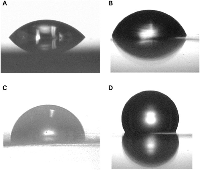
Figure 1. Water contact angle measured on electropolished copper foil (A), (C) and oxidized (B), (D) Cu substrates before and after self-assembly of a BPT monolayer.
The oxidized substrates showed a similar result, as seen from the comparison of Figures 1B, D): the BPT-functionalized oxidized Cu exhibits a CA of (114 ± 2)o, which is higher than that observed for the substrate prior to functionalization (76 ± 2)o. The difference in the contact angle between the BPT SAMs on electropolished and oxidized Cu depends on the intermolecular forces between molecules. In fact, Ron et al. (1998) and Laibinis and Whitesides (1992) reported that lower CA values are indicative of less densely packed SAMs. Consequently, our results suggest a more closely packed arrangement of the SAMs on the oxidized Cu surface.
Our observations for the bare oxidized substrate align with those of Gottardi et al. (2015), who oxidized Cu (111) in air and identified the formed oxide phase as Cu2O. Indeed, the contact angle determined for the bare oxidized surface is consistent with that (70 ± 2)° reported by Cabrita et al. (2010) for Cu2O, while these authors also found that the CAs for oxides like CuO and CuO/Cu(OH) are smaller. Hence, based on the value of the contact angle, we deduce that the oxide phase present in copper in our studies is primarily Cu2O.
To corroborate the structural integrity of the BPT molecules in the SAMs, X-ray photoelectron spectroscopy (XPS) was carried out. Figures 2A, B display the Cu2p3/2 core level region for a pristine BPT SAM on electropolished and oxidized surfaces, respectively. Two components are discernible in these spectra: the main component at 932.7 eV and a shoulder attributable to Cu bound to S at 933.5 eV. Concerning the former, we note that since both Cu and Cu2O exhibit a main component at this same binding energy (Ron et al., 1998), a precise differentiation between these oxidation states proves challenging. However, for oxidized copper (Figure 2B), the main component displays a slightly larger full width at half maximum (FWHM)—0.67 eV for oxidized and 0.6 eV for electropolished Cu—and a wider scan of the Cu2p core level region (Supplementary Figure S1) also shows a small satellite peak at around 945 eV in binding energy. Both the higher FWHM and the presence of the small satellite peak are characteristic of Cu2O, consistent with the contact angle measurements. The fact that a component due to Cu-S bonds can be discerned, points to the formation of thiolates.
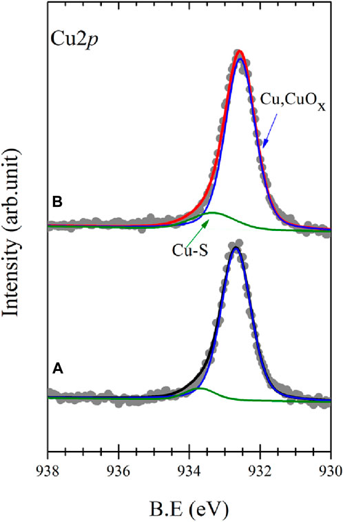
Figure 2. XPS spectra of the Cu2p3/2 core level region of a self-assembled monolayer of BPT on electropolished (A) and oxidized copper (B); raw data (●) and fit (—).
Figures 3, 4 display the C1s (left panels) and S2p (right panels) spectra for BPT self-assembled monolayers on electropolished and oxidized copper as prepared, after photopolymerization and after annealing.
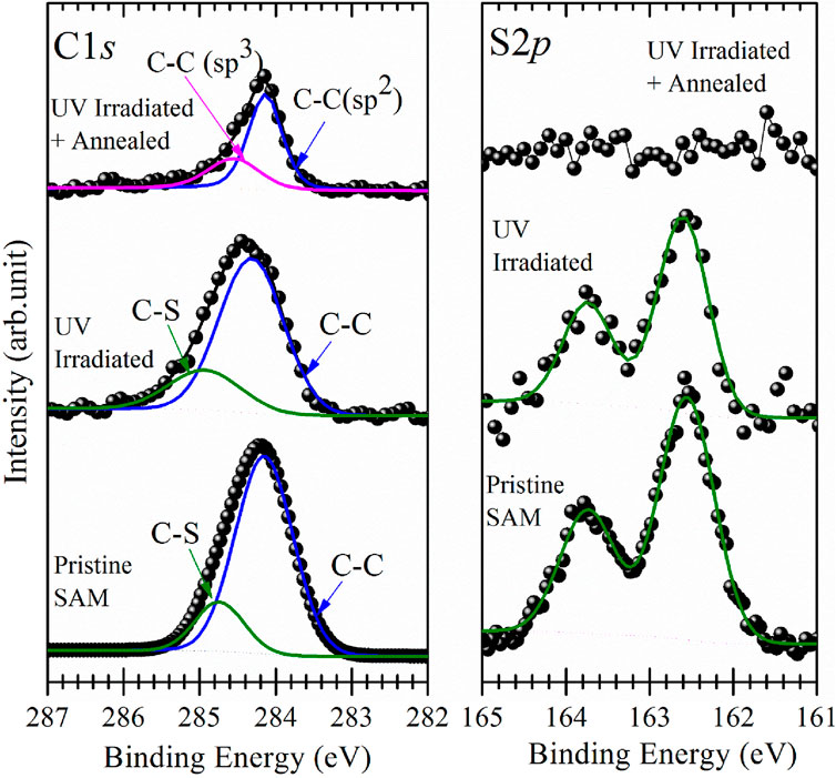
Figure 3. XPS spectra of the C1s (left panel) and S2p (right panel) core level regions of self-assembled monolayers of BPT on electropolished copper foil as prepared (bottom), after irradiation with UV light for 6 h, and after annealing to 1,100 K; raw data (●) and fit (—).
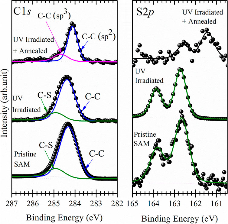
Figure 4. XPS spectra of the C1s (left panel) and S2p (right panel) core level regions of self-assembled monolayers of BPT on oxidized copper foil as prepared (bottom), after irradiation with UV light for 6 h, and after annealing to 1,100 K; raw data (●) and fit (—).
For the as-prepared BPT SAM on electropolished copper, the C1s photoemission line (Figure 3, left panel, bottom spectrum) exhibits a main component at a binding energy of 284.2 eV, attributed to the aromatic carbon of the biphenyl rings, and a smaller component due to the C-S bonds at 284.8 eV (Matei et al., 2013). Remarkably, the C1s spectrum for the as-prepared BPT SAM on oxidized copper (Figure 4, left panel, bottom spectrum) is nearly identical, with the main component at a BE of 284.3 eV and the smaller component due to C-S bonds at 284.9 eV. The S2p intensity peaks are at 162.5 eV (Figure 3, right panel) for the BPT SAM on electropolished copper and at 162.6 eV (Figure 4, right panel) for the BPT-SAM on oxidized copper, indicating the formation of thiolates (Laibinis et al., 1991) in both cases. Notably, no evidence for oxidized sulfur or metal sulfides was found at higher binding energies, confirming the structural integrity of the BPT molecules on both surfaces.
If the SAM is well-packed, the photoelectrons from the S atoms will be attenuated when passing through the biphenyl layer. To evaluate the attenuation of these photoelectrons, we calculated the intensity ratio IC1s/IS2p for both BPT SAMS and found IC1s/IS2p = 9:1 for the one on electropolished Cu and IC1s/IS2p = 8:1 for that on oxidized Cu. The lower ratio observed for the latter suggests that S2p photoelectrons experience less attenuation by the SAM, indicating a configuration where the molecules are more inclined toward the substrate surface because the adsorption sites are farther apart, and the biphenyl layer is, therefore, thinner. Such a scenario has been observed for oxidized Cu(111), where the oxide is arranged in a distorted Cu(100)-(√2x√2)R45° superstructure (Gottardi et al., 2015). Although the surfaces are polycrystalline in the present case (vide infra), it is reasonable to infer that the distinct IC1s/IS2p ratios arise from a different packing of BPT on the two surfaces. The XPS results, therefore, support the successful deposition of well-organized SAMs on both substrates, as corroborated by the contact angle measurements.
Following self-assembly and XPS characterization, the SAMs were polymerized with UV light. The polymerization step is needed to prevent desorption of individual BPTs from the surface during annealing (Matei et al., 2013), the essential step for the transformation of the SAM into graphene. To find out the optimal irradiation time, the samples were exposed to UV light (He I = 21.22 eV) for durations ranging from 1 to 12 h.
Pristine BPT SAMs and UV-irradiated (polymerized) samples show no major differences in the C1s and S2p spectra presented in Figures 3, 4. Since UV light causes emission of secondary electrons, it is reasonable to assume that the same effects as observed for electron beam irradiation occur (Turchanin et al., 2009; Yildirim et al., 2017), namely, dehydrogenation and cross-linking of the phenyl rings in such a way that they maintain their aromatic structure. For both substrates, the main C1s component shifted to a slightly higher BE (0.2 eV for the SAM on electropolished and 0.1 eV for the SAM on oxidized Cu foil). The decrease in the S2p spectral intensity, and hence in the amount of sulfur, was negligible after polymerization, and like for the C1s photoemission line, we saw a small shift (0.1 eV) of the S2p line to a higher BE after UV irradiation.
After photopolymerization, each SAM was subjected to annealing at 1,100 K. Thereafter, the carbon remaining on the surface was assessed using XPS as a function of UV irradiation time, as depicted in Figure 5 for the SAM on electropolished Cu. Notably, the sample that remained unexposed to light experienced nearly complete carbon loss during annealing. For samples irradiated for 2 or 4 h, an 80% decrease in the C1s intensity indicated incomplete polymerization of the SAM after 4 h of irradiation. Longer irradiation times (5–12 h) resulted in approximately 35% of the initial carbon remaining on the surface after annealing. This percentage closely aligns with the 30% reported by Matei et al. (2013) after electron-induced polymerization followed by annealing. Given that irradiation times exceeding 6 h did not yield a difference in the resulting carbon coverage, 6 h of irradiation was deemed sufficient.
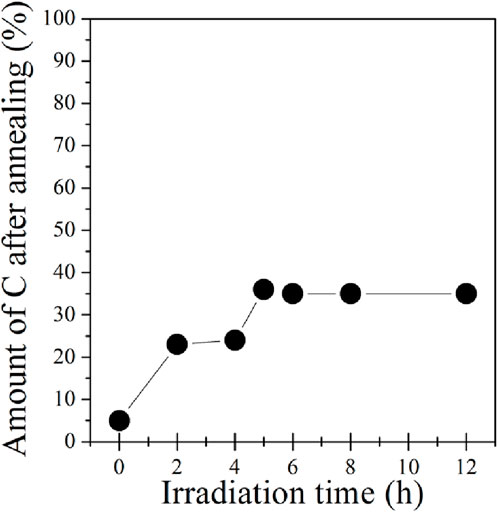
Figure 5. Relative amount of carbon remaining after annealing to 1,100 K of BPT SAMs on an electropolished copper foil that had been previously polymerized by UV irradiation, plotted as a function of UV irradiation time. 100% corresponds to the amount of carbon detected for the freshly assembled BPT before light exposure and annealing.
The top curves in Figures 3, 4 present the C1s and S2p XPS spectra collected after annealing of the polymerized SAMs. While the amount of carbon on the surface did not change with polymerization, for the annealed samples, a loss of C was evident. To estimate the changes in carbon intensities, we used the ratio of the C and Cu XPS signals IC1s/ICu2p. For the sample on oxidized Cu, a value of 0.98 was found. For reference purposes, we also prepared graphene on electropolished Cu by chemical vapor deposition (CVD), following the procedure described in Gottardi et al. (2015), which yields a single layer of graphene, and found an intensity ratio IC1s/ICu2p of 0.97 for this sample. Since the Cu intensity is attenuated by the oxide on oxidized Cu, we can conclude that there is slightly more than a single layer of carbon on the oxidized Cu surface after annealing the polymerized BPT SAM. In contrast, for BPT molecules on electropolished copper foils, after polymerization and annealing, the IC1s/ICu2p ratio is found to be 0.56, significantly lower than for CVD-grown graphene on the same surface. A possible reason for such a reduced amount of carbon is desorption of non-polymerized molecules (Turchanin et al., 2013). We cannot be certain whether it is the UV photons or the secondary electrons or both that cause polymerization in our case; however, since the secondary electron yield of Cu is higher than that for copper oxides (Aguilera et al., 2013), if only secondary electrons were involved, there should be more non-polymerized BPT on oxidized copper than on electropolished Cu.
For the C1s lineshape, we first observe that the full width at half maximum (FWHM) of the main component of the annealed photopolymerized SAM on electropolished Cu (Figure 3, left panel, top curve) as well as on oxidized Cu (Figure 4 left panel top curve) has decreased to half the value it had in after polymerization and amounts now to 0.5 eV. Since the lineshape and binding energy of both samples very closely resemble those of CVD-grown graphene (Bignardi, 2013), we attribute the main component to sp2-hybridized carbon and the smaller component to sp3-hybridized carbon.
As seen in Figure 4 (right panel, top curve), sulfur is detected in the XPS spectrum after annealing the photopolymerized BPT SAM on oxidized copper, while no traces of sulfur were found for the one on electropolished copper foils (Figure 3, right panel, top curve). Compared to the spectrum before annealing, the sulfur signal shows a 65% decrease in the intensity, and the peak maximum shifts to a BE of 161.5 eV, typical of copper sulfides. This confirms the breaking of C-S bonds during annealing (Matei et al., 2013), as already concluded from the shape of the C1s photoemission line of the photopolymerized BPT SAM on oxidized copper. It is reasonable to assume that because of the higher amount of carbon present on the oxidized surface after annealing, sulfur atoms are blocked by the carbon layer on top and cannot desorb even at high temperatures, while on electropolished copper, they can easily desorb because the carbon layer is incomplete.
From CA and XPS measurements of the polymerized and annealed BPT SAMs, the presence of graphitized carbon was established. To ascertain whether the carbon layer is indeed graphene, Raman spectroscopy was performed. Graphene typically exhibits distinct Raman features, namely, the D band, the G band, and the Gʹ band (Ferrari et al., 2006; Malard et al., 2009). The D band is a measure of the number of defects and, therefore, provides an insight into the quality of the material, while the position and shape of the Gʹ band as well as the ratio between the intensities of the G and the G’ bands give information about the number of graphene layers (Ferrari et al., 2006; Malard et al., 2009; Lucchese et al., 2010). A ratio IG'/IG ∼ 2–3 is found for monolayer graphene, 2 > IG'/IG > 1 for bilayer graphene, and IG'/IG < 1 for multilayer graphene. Figure 6 presents the Raman spectra acquired on the polymerized BPT SAMs on electropolished (black curve) and oxidized copper foil (red curve) after annealing. The relative intensity and position of the peaks were consistent throughout each sample. One can clearly see the fingerprints of graphene: the G band at 1,607 cm−1, the D band at 1,335 cm−1, and the Gʹ band at 2,672 cm−1. For graphene grown on oxidized copper, the ratio IG'/IG is ∼ 2, pointing to a single layer of graphene. The lower intensity of the D band indicates that graphene grown on oxidized copper foil has fewer defects and, therefore, is of better quality than that grown on electropolished copper. The average distance between two point defects in the graphene layer was estimated using the intensity ratio of the G and D peaks (Lucchese et al., 2010). For the graphene on the oxidized substrate, the ratio ID/IG ∼ 0.3 implies an average distance between point defects of ca. 20 nm, while for electropolished substrates, ID/IG ∼ 1.1 gives an average distance of ca. 10 nm. These results align with the findings of Gottardi et al. 2015, who demonstrated that CVD-grown graphene on oxidized Cu(111) is of higher quality than that grown on electropolished substrates. Furthermore, analysis of the Gʹ band of graphene on oxidized copper foil (red curve) shows that it can be fitted with a single Lorentzian with a full width at half maximum of 46 cm−1, confirming single-layer graphene growth (Ferrari et al., 2006; Bignardi et al., 2013) already deduced from the XPS results.
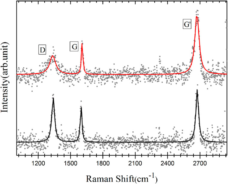
Figure 6. Raman spectra acquired after annealing photo-polymerized 1, 1ʹ, biphenyl-4-thiol SAMs on electropolished (black curve) and oxidized copper foil (red curve); raw data (●) and fit (—).
To explore the morphological properties of graphene grown on both substrates, we performed scanning electron microscopy. Figure 7A displays the SEM image of graphene grown on electropolished copper foil. As already inferred from the XPS data, graphene does not form a continuous layer. Instead, the island density varies depending on the grain orientations of the foil. These results are consistent with graphene grown by chemical vapor deposition (CVD) on polycrystalline copper foil (Wood et al., 2011), where the most favorable orientation for graphene growth is Cu(111), followed by growth on high-index facets, while Cu(100) has been identified as the least favorable orientation with a slow graphene growth rate. In Figure 7A, three large distinct crystalline orientations are observed. The grain at the bottom left of the image exhibits continuous film growth with only few very small holes in the film, while other grains clearly show island formation. To understand these morphological differences, we determined the structure of the copper surface using electron backscattering diffraction (EBSD), as shown in Figure 8A. We found that the electropolished Cu foil consists of multiple orientations, with grain sizes ranging between 50 and 100 µm. Approximately 28% of the grains were oriented (001), 11% (101) and 2.5% (111), while the rest of the area consisted of high-index facets. The grains exhibiting island growth (Figure 7A) were closer to Cu(100) in orientation than the grains exhibiting continuous growth, which was close to Cu(111). This proves that the reduced diffusion on Cu(100) (Wood et al., 2011) is reflected also in the quality of the graphene produced by our method. Figure 7B shows the SEM image of graphene grown by annealing the polymerized BPT SAM on oxidized copper. Here, the layer is continuous and covers the entire surface; no holes can be seen. This explains the lower defect density deduced from the Raman spectra.
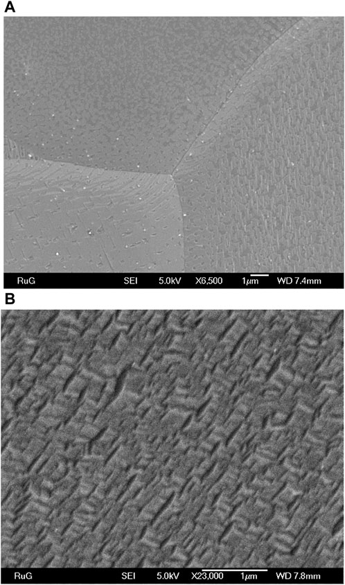
Figure 7. Scanning electron microscopy of (A) graphene on electropolished Cu foil and (B) graphene on Cu2O/Cu foil produced by annealing a photo-polymerized BPT SAM.
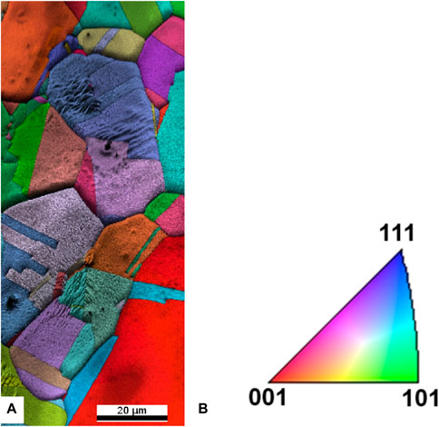
Figure 8. Electron backscattering diffraction map obtained on graphene on electropolished Cu foil (A) and the relation between false color coding and crystallographic orientation (B).
Further details concerning the structural properties of the grown graphene can be gained from transmission electron microscopy. For this purpose, the graphene layer needs to be transferred to TEM grids, as described in Bignardi et al. (2013). We were unable to transfer graphene grown on electropolished copper as it was not a continuous film, and graphene islands spread in the etchant solution. The graphene grown on oxidized copper was successfully transferred. Figure 9A shows the TEM micrograph of the suspended graphene; more than 90% of the 2-µm holes are covered. During transfer to the TEM grid, the sheets can fold or break, as seen in Figure 9A, where one hole is not fully covered and the rupture in the sheet is indicated with a blue arrow. During the transfer procedure, some defects like wrinkles and folding of sheets can occur (Bignardi et al., 2013); Figures 9A, B provides a detailed view of suspended graphene, revealing a wrinkle in the graphene sheet. The electron diffraction pattern collected from this sample is presented in Figure 9C. After background subtraction (Figure 9D), a single set of hexagonal spots is visible, indicating that the graphene layer is single crystalline in the measured region. However, this observation is not representative of the entire graphene layer; in fact, only 10% of the free-standing graphene in the 2-µm-diameter circular holes was found to be a single domain, and 90% exhibited a multidomain structure, explaining the observed defect peak D intensity in the Raman data.
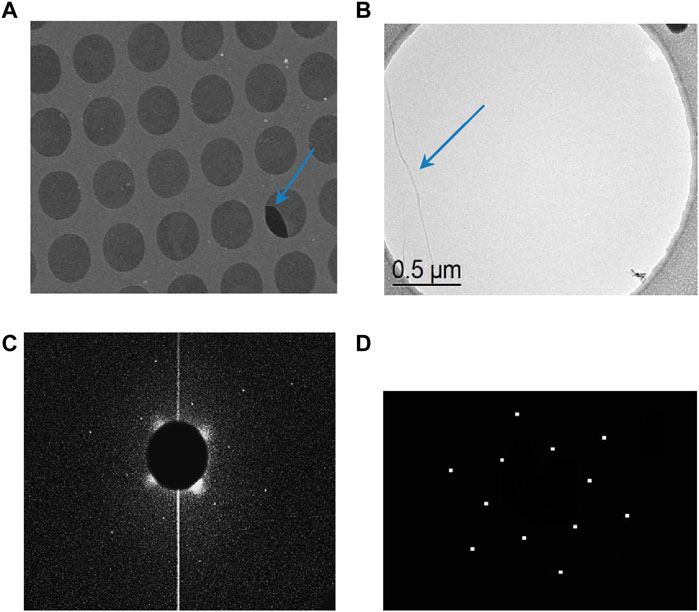
Figure 9. TEM of graphene grown by annealing a polymerized BPT SAM on oxidized Cu and transferred to TEM grids. (A) Overview of approximately 250 μm2 area of the TEM grid; (B) detailed image of a single layer of suspended graphene; (C) electron diffraction pattern obtained on the area shown in panel (B); (D) same electron diffraction pattern as (C) after background subtraction.
4 Conclusion
In conclusion, we developed an improved method for graphene synthesis on copper foils through the annealing of self-assembled monolayers of 1,1ʹ-biphenyl-4-thiol, previously polymerized using UV light rather than an electron beam. On the electropolished Cu foil, we found that the quality of the obtained graphene strongly depends on the crystallographic orientation of the grains, and a continuous layer was obtained only on Cu(111), while other orientations showed growth of small islands. Interestingly, oxidized Cu foils yielded superior graphene quality with the formation of a continuous layer and approximately 10% of the grains exceeding 2 μm in size. However, it is noteworthy that achieving such high-quality graphene required temperatures comparable to those used in CVD growth. This synthesis route opens the way for graphene preparation via self-assembly of precursor molecules on insulating substrates, provided they exhibit similar catalytic properties leading to graphitization, as observed with the Cu2O surface studied in this work. The next challenge will be to verify whether this method is also suitable for producing doped graphene and, if yes, whether a certain arrangement of the doping atoms in the precursor molecule can be preserved in the resulting graphene.
Data availability statement
The original contributions presented in the study are included in the article/Supplementary Material; further inquiries can be directed to the corresponding author.
Author contributions
TZ: data curation, formal analysis, funding acquisition, investigation, validation, visualization, writing–original draft, and writing–review and editing. AS: data curation, formal analysis, investigation, writing–original draft, and writing–review and editing. OI: data curation, formal analysis, investigation, writing–original draft, and writing–review and editing. LB: data curation, investigation, writing–original draft, and writing–review and editing. WV: data curation, formal analysis, investigation, writing–original draft, and writing–review and editing. JH: resources, supervision, validation, writing–original draft, and writing–review and editing. PR: conceptualization, methodology, project administration, resources, supervision, validation, writing–original draft, and writing–review and editing.
Funding
The author(s) declare that financial support was received for the research, authorship, and/or publication of this article. TZ acknowledges the Schlumberger Foundation’s Faculty for the Future program for supporting her PhD study. This work was performed within the “Top Research School” program of the Zernike Institute for Advanced Materials under the Bonus Incentive Scheme (BIS) of the Netherlands’ Ministry of Education, Science, and Culture.
Acknowledgments
The authors thank Wesley R. Browne for support with the Raman measurements and Petra Reinke for insightful discussions. Preliminary studies by the bachelor students Roban van Herk, André Mintjes, and Estela Moretón Alfonsin are gratefully acknowledged.
Conflict of interest
The authors declare that the research was conducted in the absence of any commercial or financial relationships that could be construed as a potential conflict of interest.
Publisher’s note
All claims expressed in this article are solely those of the authors and do not necessarily represent those of their affiliated organizations, or those of the publisher, the editors, and the reviewers. Any product that may be evaluated in this article, or claim that may be made by its manufacturer, is not guaranteed or endorsed by the publisher.
Supplementary material
The Supplementary Material for this article can be found online at: https://www.frontiersin.org/articles/10.3389/fnano.2024.1366542/full#supplementary-material
References
Aguilera, L., Montero, I., Dávila, M. E., Ruiz, A., Galán, L., Nistor, V., et al. (2013). CuO nanowires for inhibiting secondary electron emission. J. Phys. D. Appl. Phys. 46, 165104. doi:10.1088/0022-3727/46/16/165104
Akinwande, D., Brennan, C. J., Bunch, J. S., Egberts, P., Felts, J. R., Gao, H., et al. (2017). A review on mechanics and mechanical properties of 2D materials—graphene and beyond. Extreme Mech. Lett. 13, 42–77. doi:10.1016/j.eml.2017.01.008
Angelova, P., Vieker, H., Weber, N.-E., Matei, D., Reimer, O., Meier, I., et al. (2013). A universal scheme to convert aromatic molecular monolayers into functional carbon nanomembranes. ACS Nano 7 (8), 6489–6497. doi:10.1021/nn402652f
Bae, S., Kim, H., Lee, Y., Xu, X., Park, J.-S., Zheng, Y., et al. (2010). Roll-to-roll production of 30-inch graphene films for transparent electrodes. Nat. Nanotechnol. 5 (8), 574–578. doi:10.1038/nnano.2010.132
Batzill, M. (2012). The surface science of graphene: metal interfaces, CVD synthesis, nanoribbons, chemical modifications, and defects. Surf. Sci. Rep. 67, 83–115. doi:10.1016/j.surfrep.2011.12.001
Belser, A., Greulich, K., Klein, M., Gruninger, P., Sättele, M. S., Fingerle, M., et al. (2023). Planar BN-doped nanographenes on reactive metal surfaces: a promising pathway for the preparation of BN-doped graphene layers. ACS Appl. Electron. Mat. 5, 5193–5201. doi:10.1021/acsaelm.3c00924
Berger, C., Song, Z., Li, T., Li, X., Ogbazghi, A. Y., Feng, R., et al. (2004). Ultrathin epitaxial graphite: 2D electron gas properties and a route toward graphene-based nanoelectronics. J. Phys. Chem. B 108, 19912–19916. doi:10.1021/jp040650f
Bignardi, L. (2013). “Electronic and structural properties of graphene/metal interphases,”. PhD thesis (Groningen, Netherlands: University of Groningen). ISNBNs 9789036762588.
Bignardi, L., van Dorp, W. F., Gottardi, S., Ivashenko, O., Dudin, P., Barinov, A., et al. (2013). Microscopic characterisation of suspended graphene grown by chemical vapour deposition. Nanoscale 5 (13), 9057–9061. doi:10.1039/C3NR02386A
Cabrita, J. F., Viana, A. S., and Abrantes, L. M. (2010). Copper protection by phosphonic acid self-assembled monolayers. Corros. Prot. Mat. 29 (4), 114–119.
Dikin, D. A., Stankovich, S., Zimney, E. J., Piner, R. D., Dommett, G. H. B., Evmenenko, G., et al. (2007). Preparation and characterization of graphene oxide paper. Nature 448, 457–460. doi:10.1038/nature06016
Emtsev, K. V., Bostwick, A., Horn, K., Jobst, J., Kellogg, G. L., Ley, L., et al. (2009). Towards wafer-size graphene layers by atmospheric pressure graphitization of silicon carbide. Nat. Mat. 8 (3), 203–207. doi:10.1038/nmat2382
Ferrari, A. C., Meyer, J. C., Scardaci, V., Casiraghi, C., Lazzeri, M., Mauri, F., et al. (2006). Raman spectrum of graphene and graphene layers. Phys. Rev. Lett. 97, 187401. doi:10.1103/PhysRevLett.97.187401
Gengler, R. Y. N., Spyrou, K., and Rudolf, P. (2010). A roadmap to high quality chemically prepared graphene. J. Phys. D. Appl. Phys. 43 (37), 374015. doi:10.1088/0022-3727/43/37/374015
Gilje, S., Han, S., Wang, M., Wang, K. L., and Kaner, R. B. (2007). A chemical route to graphene for device applications. Nano Lett. 7 (11), 3394–3398. doi:10.1021/nl0717715
Gottardi, S., Müller, K., Bignardi, L., Moreno-López, J. C., Pham, T. A., Ivashenko, O., et al. (2015). Comparing graphene growth on Cu(111) versus oxidized Cu(111). Nano Lett. 15 (2), 917–922. doi:10.1021/nl5036463
Laibinis, P. E., and Whitesides, G. M. (1992). Self-assembled monolayers of n-alkanethiolates on copper are barrier films that protect the metal against oxidation by air. J. Am. Chem. Soc. 114, 9022–9028. doi:10.1021/ja00049a038
Laibinis, P. E., Whitesides, G. M., Allara, D. L., Tao, Y.-T., Parikh, A. N., and Nuzzo, R. G. (1991). Comparison of the structures and wetting properties of self-assembled monolayers of n-alkanethiols on the coinage metal surfaces, copper, silver, and gold. J. Am. Chem. Soc. 113 (19), 7152–7167. doi:10.1021/ja00019a011
Li, X., Cai, W., An, J., Kim, S., Nah, J., Yang, D., et al. (2009). Large-area synthesis of high-quality and uniform graphene films on copper foils. Science 324, 1312–1314. doi:10.1126/science.1171245
Lucchese, M. M., Stavale, F., Martins Ferreira, E. H., Vilani, C., Moutinho, M. V. O., Capaz, R. B., et al. (2010). Quantifying ion-induced defects and Raman relaxation length in graphene. Carbon 48, 1592–1597. doi:10.1016/j.carbon.2009.12.057
Malard, L. M., Pimenta, M. A., Dresselhaus, G., and Dresselhaus, M. S. (2009). Raman spectroscopy in graphene. Phys. Rep. 473 (5-6), 51–87. doi:10.1016/j.physrep.2009.02.003
Matei, D. G., Weber, N.-E., Kurasch, S., Wundrack, S., Woszczyna, M., Grothe, M., et al. (2013). Functional single-layer graphene sheets from aromatic monolayers. Adv. Mat. 25 (30), 4146–4151. doi:10.1002/adma.201300651
Novoselov, K. S., Falʹko, V. I., Colombo, L., Gellert, P. R., Schwab, M. G., and Kim, K. (2013). A roadmap for graphene. Nature 490, 192–200. doi:10.1038/nature11458
Novoselov, K. S., Geim, A. K., Morozov, S. V., Jiang, D., Katsnelson, M. I., Grigorieva, I. V., et al. (2005). Two-dimensional gas of massless Dirac fermions in graphene. Nature 438, 197–200. doi:10.1038/nature04233
Novoselov, K. S., Geim, A. K., Morozov, S. V., Jiang, D., Zhang, Y., Dubonos, S. V., et al. (2004). Electric field effect in atomically thin carbon films. Science 306, 666–669. doi:10.1126/science.1102896
Rhinow, D., Weber, N. E., and Turchanin, A. (2012). Atmospheric pressure, temperature-induced conversion of organic monolayers into nanocrystalline graphene. J. Phys. Chem. C 116 (22), 12295–12303. doi:10.1021/jp301877p
Ron, H., Cohen, H., Matlis, S., Rappaport, M., and Rubinstein, I. (1998). Self-assembled monolayers on oxidized metals. 4. superior n -alkanethiol monolayers on copper. J. Phys. Chem. B 102 (49), 9861–9869. doi:10.1021/jp9827072
Turchanin, A., Käfer, D., El-Desawy, M., Wöll, C., Witte, G., and Gölzhäuser, A. (2009). Molecular mechanisms of electron-induced cross-linking in aromatic SAMs. Langmuir 25 (13), 7342–7352. doi:10.1021/la803538z
Turchanin, A., Weber, D., Büenfeld, M., Kisielowski, C., Fistul, M. V., Efetov, K. B., et al. (2011). Conversion of self-assembled monolayers into nanocrystalline graphene: structure and electric transport. ACS Nano 5 (5), 3896–3904. doi:10.1021/nn200297n
Wang, X., Zhi, L., and Müllen, K. (2008). Transparent, conductive graphene electrodes for dye-sensitized solar cells. Nano Lett. 8 (1), 323–327. doi:10.1021/nl072838r
Wood, J. D., Schmucker, S. W., Lyons, A. S., Pop, E., and Lyding, J. W. (2011). Effects of polycrystalline Cu substrate on graphene growth by chemical vapor deposition. Nano Lett. 11 (11), 4547–4554. doi:10.1021/nl201566c
Yildirim, C., Füser, M., Terfort, A., and Michael Zharnikov, M. (2017). Modification of aromatic self-assembled monolayers by electron irradiation: basic processes and related applications. J. Phys. Chem. C 121 (1), 567–576. doi:10.1021/acs.jpcc.6b11269
Keywords: graphene growth, bi-phenylthiol, self-assembled monolayers, photopolymerization, X-ray photoelectron spectroscopy, Raman spectroscopy, transmission electron microscopy, contact angle measurements
Citation: Zehra T, Syari’ati A, Ivashenko O, Bignardi L, Van Dorp WF, De Hosson JTM and Rudolf P (2024) Graphene growth from photo-polymerized bi-phenylthiol self-assembled monolayers. Front. Nanotechnol. 6:1366542. doi: 10.3389/fnano.2024.1366542
Received: 06 January 2024; Accepted: 11 March 2024;
Published: 04 April 2024.
Edited by:
Neha Kaushik, University of Suwon, Republic of KoreaReviewed by:
Rita Rizzoli, CNR—Institute for Microelectronics and Microsystems (IMM), ItalyCarla Bittencourt, University of Mons, Belgium
Copyright © 2024 Zehra, Syari’ati, Ivashenko, Bignardi, Van Dorp, De Hosson and Rudolf. This is an open-access article distributed under the terms of the Creative Commons Attribution License (CC BY). The use, distribution or reproduction in other forums is permitted, provided the original author(s) and the copyright owner(s) are credited and that the original publication in this journal is cited, in accordance with accepted academic practice. No use, distribution or reproduction is permitted which does not comply with these terms.
*Correspondence: Petra Rudolf, cC5ydWRvbGZAcnVnLm5s