 Rajib Ratan Ghosh
 Danqing Liu2
- 1Department of Electrical Engineering, Eindhoven University of Technology, Eindhoven, Netherlands
- 2Department of Chemical Engineering and Chemistry, Eindhoven University of Technology, Eindhoven, Netherlands
Artificial neural networks (ANNs) have become ubiquitous in high-performance information processing. However, conventional electronic hardware, based on the sequential Von Neumann architecture, struggles to efficiently support ANN computations due to their inherently massive parallelism. Additionally, electrical parasitics further limit energy efficiency and processing speed, pushing traditional architectures toward their fundamental constraints. To overcome these limitations, researchers are exploring integrated photonics, leveraging the inherent parallelism of optical devices for more efficient computation. Despite these efforts, most existing optical computing schemes encounter scalability challenges, given that the number of optical elements typically grows quadratically with the computational matrix size. In this work, a compact programmable multimode interference (MMI) coupler on an indium phosphide membrane platform is proposed for realizing a photonic feedforward neural network. MMIs present a unique opportunity to accelerate matrix multiplication processes by exploiting the interference properties of light modes, promising advancements in both speed and energy efficiency. The programmable MMI coupler, comprising four input and three output (4 × 3 MMI) InP waveguides, makes use of hybrid integration of liquid crystals as cladding material, which offers reconfigurability to the MMI structure. Three electrically tunable sections are made to perform parallel multiplication operations. A novel modeling technique is introduced to facilitate effective training and inference operations. Finite-Difference Time-Domain (FDTD) simulations are employed for calculating the optical mode propagation process within the programmable MMI structure. Based on the FDTD results, a compact optical neural network is implemented and assessed on the Iris flower dataset, demonstrating a testing accuracy of 86.67%. This novel MMI device concept offers a promising pathway toward energy-efficient, scalable optical computing systems, contributing to the advancement of next-generation artificial intelligence hardware.
1 Introduction
In the dynamic landscape of artificial neural network (ANN) applications, the demand for efficient and high-speed computational frameworks is growing rapidly (Sze et al., 2017). While traditional electronic computing continues to advance, it faces fundamental bottlenecks—such as high power consumption and limited speed—particularly when scaling to large matrix operations required by ANN algorithms (Jouppi et al., 2017). Optical neural networks (ONNs) have emerged as a promising alternative by leveraging light’s unique properties to overcome these challenges (Liao et al., 2023; Shastri et al., 2021). Unlike electronic neural networks, ONNs exploit light’s inherent parallelism, enabling simultaneous execution of multiple operations, thereby significantly improving computational throughput and energy efficiency. However, contemporary photonic hardware still faces scalability and integration challenges, as optical computing approaches often suffer from quadratic growth in optical elements with increasing matrix size (Bai et al., 2023). Integrated photonics plays a crucial role in overcoming these limitations by enabling compact, high-density optical circuits that facilitate interconnectivity and large-scale integration. ONNs harness various properties of light—such as phase, amplitude, wavelength, modes, and polarization—to achieve a high degree of parallelism in computation (Feldmann et al., 2021). Additionally, photonic systems benefit from large bandwidth, low propagation losses, and efficient light-matter interactions, leading to energy-efficient operations (<pJ per multiply operation) and ultrafast processing speeds (>1012 operations per second) (Bai et al., 2023; Feldmann et al., 2021; Guo et al., 2021; Shen et al., 2017; Nahmias et al., 2018; Xu et al., 2021; Dabos et al., 2022; Giamougiannis et al., 2021). These advantages position ONNs as a compelling alternative to electronic counterparts, paving the way for next-generation artificial intelligence (AI) accelerators that meet the growing computational demands of modern AI applications. Active research is underway in the domain of photonic matrix multiplication devices, with many relying on free space optics incorporating dynamic mirror devices (DMDs) (Zhou et al., 2022), spatial light modulators (SLMs) (Zhou et al., 2021), or principles of Fourier optics (Von Bieren, 1971). However, scaling these systems to meet impeding computational demands proves challenging due to their substantial size (Zhou et al., 2022). Several innovative concepts propose the use of networks featuring optical interferometers (Shen et al., 2017; Zhang et al., 2021), ring resonators (Tait et al., 2017; Miscuglio and Sorger, 2020), amplifiers (Shi et al., 2019; Ferreira de Lima et al., 2017), or phase change materials (Feldmann et al., 2021; Cheng et al., 2017), which are conducive to miniaturization and integration onto a photonic chip. The field of integrated neuromorphic photonics is dynamic, and there is a strong need for pioneering concepts that can provide future energy-efficient and high-speed computational hardware. In this work, we propose leveraging multi-mode interference (MMI) between waveguide modes to perform matrix multiplication within a programmable MMI coupler. MMI couplers are typically constructed from wide optical waveguides that provide transverse light confinement, supporting multiple propagating modes beyond the fundamental mode (Soldano and Pennings, 1995). Based on the self-imaging or Talbot effect, MMIs have been extensively used in photonic integrated circuits (PICs) for couplers, splitters, combiners, and other passive optical functions (Bachmann et al., 1995; Samoi et al., 2020; Peruzzo et al., 2011). However, their potential for neuromorphic computation remains largely unexplored, with only a few studies investigating their suitability. Most existing works utilize MMIs for reconfigurable photonic routing between input and output waveguides or as passive interference elements in conjunction with optical phase shifters for weighting matrix operations (Soures et al., 2018; Wu et al., 2023; Meng et al., 2023; Shixin et al., 2025). Here, we have demonstrated matrix-vector multiplication using a single electrically reconfigurable MMI coupler. Any input field to the MMI is projected onto the system modes, which then evolve according to their respective propagation constants within the multi-mode region. At any position along the MMI, the total field is a superposition of all system modes. The presence of numerous system modes in MMIs makes them well-suited for parallel computation, as these modes interact and interfere with each other. This interaction produces intricate interference patterns, enabling precise manipulation and control of the output optical field distribution. The optical mode in each input waveguide represents an individual input signal, while the full set of input waveguide modes forms an input vector. The propagation of these modes through the MMI corresponds to the computational operation. In conventional MMIs, the coupling from the input field to the system modes and the propagation constants are determined by the geometry and are usually fixed after fabrication. The MMI needs to be pre-designed to fulfill a certain function (splitter, switch, etc.). If there is a means to selectively alter the refractive index at some specific positions along the propagation and transverse directions of the MMI device, we are able to reconfigure the MMI device. In contrast to inverse design methods (Tahersima et al., 2019), we want to be able to perform this after fabrication in a reconfigurable manner. We propose a reconfigurable MMI coupler wherein some sections of the MMI device need to be segmented into ‘pads’ with accurate local refractive index control. The homogeneous multi-mode area can be reconfigured to be inhomogeneous, and hence the mode propagation expression is altered. In particular, the mode coupling coefficients, together with the propagation term can act as a weight that is applied to the transverse modes, performing matrix multiplication. In this work, we focus on the implementation of the reconfigurability of the MMI coupler by introducing electrically tunable liquid crystals (LC) integrated as a top cladding to the MMI device. Liquid crystals are molecularly ordered materials with well-controlled molecular positioning into all three dimensions (Liu and Broer, 2014; Fukuhara et al., 2014; Xing et al., 2015). Those different types of alignments can be established by surface orientation techniques and chiral additives. LCs exhibit unique, highly adjustable, and addressable optical, electrical, and mechanical properties. Their dielectric anisotropy makes them electro-responsive and enables precise control over light transmission. These electro-optic properties have been widely explored, most notably in liquid crystal display LCD technology. Figure 1 illustrates the conceptual design and operational principle of a programmable multimode interference (MMI) coupler integrated with electrically controlled liquid crystal (LC) molecules. The MMI coupler receives an input optical signal, represented as [X], which is projected onto a set of system modes that propagate through the multimode region with distinct propagation constants. The total optical field within the MMI is a superposition of these modes, allowing for complex interference patterns to emerge. A key feature of this system is the integration of an LC cell, which enables dynamic phase modulation. The refractive index of the LC molecules changes in response to an applied voltage, leading to controlled phase shifts that alter the optical field distribution (Lee et al., 2023). The figure highlights this process by depicting the initial alignment of LC molecules in their default state and their reorientation under an applied electric field, which modifies the optical transmission properties of the MMI region. As the optical modes propagate, their interference patterns are influenced by these voltage-induced phase shifts, enabling precise control over the output optical signals, denoted as [Y]. This interaction effectively performs matrix-vector multiplication, where the weight matrix Wij(V) is governed by the LC-induced phase modulation. This programmable optical platform offers an efficient approach for reconfigurable photonic computing, making it well-suited for applications in neuromorphic computing, programmable photonics, and high-speed signal processing. We propose a novel device and integration concept for LC on InP membrane photonics for neuromorphic computing. It is well known that the refractive index of LCs can be modulated by altering their molecular alignment, characterized by the director, under an applied electric field (Lee et al., 2023). In this study, we introduce a novel approach involving a compact, reconfigurable, and programmable 4 × 3 Multimode Interference (MMI) cell implemented on an InP membrane platform (Jiao et al., 2020a), designed to execute optical neural network operations in a fully parallel manner. The integration of liquid crystal atop the waveguide, serving as an electro-optic cladding material, facilitates significant tuning in the output waveguides. By leveraging wavelength division multiplexing (WDM) technology and multimode interference coupling, the MMI cell—equipped with multiple control pads—processes multiple wavelength- and amplitude-encoded input signals, enabling simultaneous linear matrix multiplication operations in a fully parallel manner. To the best of our knowledge, the integration of LC tuning within a MMI coupler on an Indium Phosphide membrane platform for neuromorphic applications is a novel concept that has not been reported in any previous literature. This study represents the first-time modeling of an optical neural network with such a device and includes benchmarking on the Iris flower dataset.
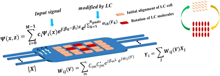
Figure 1. Conceptual illustration and operational principle of the programmable MMI coupler, where electrically controlled LC molecules modify light propagation. The optical field evolution is defined by several parameters: M denotes the number of supported optical modes, ci represents the amplitude coefficients, and Ψi is the transverse mode profiles. The propagation constants are given by β0, βi and z represents the propagation distance. The number of tuning pads is Npads, with αik(Vk) denoting the phase shift induced by the applied voltage Vk. The synaptic weight matrix formulation involves the mode coupling coefficients Cim and Cjm, where βm is the propagation constant of mode m, L is the length of the MMI region, and ϕij(V) represents the voltage-controlled phase shift. Descriptions of all variables are provided in Supplementary Table S2 in Supplementary Note 3.
2 Device architecture and design
The proposed device is a programmable multimode interference (MMI) coupler specifically designed for the Iris flower classification task. A 4 × 3 MMI coupler configuration is selected to align with the dataset structure, accommodating the four input features and three classification categories of the Iris flower dataset. The programmable MMI coupler consists of three primary components: the input tapered waveguides, a wider MMI core with hybrid integration of liquid crystal (LC) within the cladding sections for dynamic reconfigurability, and the output tapered waveguides. The input waveguides are tapered from 0.4 µm to 2 μm, facilitating efficient coupling of the fundamental optical mode into higher-order modes within the MMI core. The core itself is a wide waveguide with a width of 11.5 µm and a length of 285 μm, acting as the primary region for optical interference. The output tapered waveguides enable effective coupling of the optical modes, with a taper width that varies from 3 μm to 0.4 µm. The overall thickness of the MMI structure is 0.3 µm, ensuring a compact design suitable for photonic integration. A schematic view and cross-sectional view of the LC-filled MMI core are shown in Figures 2a, b, with detailed dimensions of the passive MMI section provided in Figure 2c. The device operates in the transverse magnetic (TM) mode, which enhances the interaction between the optical field and the LC cladding, providing stronger tuning capability compared to the transverse electric (TE) mode. The propagation lengths of the optical modes within the MMI core are designed to ensure sufficient space for interaction with metal pads and interference of optical modes. These metal pads function as electrodes that apply an electric field to the LC cladding, modulating the refractive index and enabling dynamic control over the output optical power distribution. While a higher number of metal pads would increase the granularity of control, it would also result in greater simulation complexity, longer simulation times, and a higher computational load. Therefore, the proposed design incorporates three metal pads, offering a balanced trade-off between controllability and practicality. However, increasing the number of control pads could enhance the device’s performance, but it would also introduce greater complexity in the electrical contacting scheme. The proposed fabrication process allows for such scalability; however, for the proof-of-concept simulation, the number of pads was reduced to three to minimize computational complexity and simulation time. This design ensures that the proposed MMI coupler remains compact, efficient, and suitable for photonic feedforward neural network implementations, particularly in the context of classification tasks such as the Iris dataset.
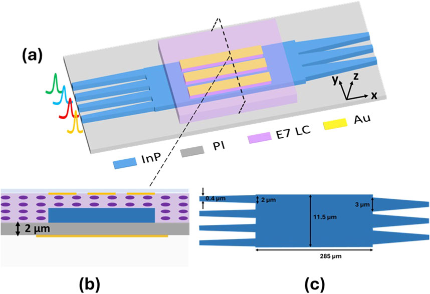
Figure 2. (a) Schematic of the proposed programmable multimode interference (MMI) coupler. (b) Cross-sectional view of the MMI coupler, showing liquid crystal filled between the waveguide and a glass plate. (c) Detailed dimensions of the passive MMI coupler structure.
Figure 3a illustrates the normalized transmission spectra for the three output waveguides when the source is positioned at the first input waveguide, highlighting the broadband nature of the MMI coupler. To evaluate the transmission response, four sources with distinct wavelengths (1,548 nm, 1,550 nm, 1,552 nm, and 1,554 nm) were considered, as shown in Figure 3b. The results indicate that the optical modes propagating through the MMI coupler experience very low insertion losses (<0.5 dB), due to the efficient coupling between the input and output waveguides via the MMI core. This suggests a favorable initial state for the MMI. Figures 3c–f show the optical field distribution for all four source positions. Transmission calculations are presented for the first and second positions, as the symmetry of the remaining positions is evident in Figure 3b and the corresponding field profiles. Note that the optical modes at the tapered output waveguide are not fundamental modes. In this study, total optical power is calculated regardless of the optical modes at the output tapered waveguides.
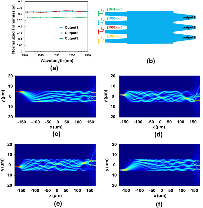
Figure 3. (a) The transmission spectra of the MMI coupler for three different output waveguides when the source is positioned at the first waveguide. (b) Separate wavelength sources are placed at input waveguides of the 4 × 3 MMI coupler. (c–f) The optical field distribution of the 4 × 3 MMI coupler for the 4 input waveguides with separate wavelength sources.
3 Liquid crystal tuning
The tunability of the proposed multimode interference (MMI) coupler is achieved by modifying the material properties around specific regions where dominant optical fields are concentrated. Optical field patterns within an MMI are typically most pronounced near the midpoint along the propagation direction (Leuthold and Joyner, 2001). In our 4 × 3 MMI coupler, this effect is particularly evident for all four input source positions at the midpoint. To enable compact and efficient phase modulation, we propose an integration scheme that combines tunable liquid crystal (LC) with the indium phosphide (InP) membrane waveguide. Figure 4a provides a cross-sectional view of this scheme, showing three gold (Au) pads used as electrodes. When external voltages are applied to these pads, an electric field is established in the LC region between the glass plate and the InP waveguide, separated by a spacer (see the inset of Figure 4a). The electrostatic field distribution in the liquid crystal (LC) region is calculated using Nextnano simulation software. This electric field reorients the director of the LC molecules, allowing dynamic modulation of the refractive index. An alignment layer sets the initial orientation of the LC director within the xy-plane. When an electric field is applied in the vertical direction, the director rotates into the z-direction from its initial position, as illustrated in Figure 4c. The initial director position is selected along the y-axis because this orientation offers a more significant change in the effective refractive index than the x-axis, a finding supported by Finite-Difference Time-Domain (FDTD) simulations. The transverse magnetic (TM) mode, chosen for this design, features a strong normal (Z) component that extends deep into the cladding, as depicted in Figure 4d. This deep penetration enhances interaction with the nematic E7 LC, which is chosen for its well-known optical anisotropy and efficient electro-optic response. Without an electric field, the director aligns in the y-direction, providing the LC with both ordinary and extraordinary dielectric constants. The effective dielectric constant of the LC layer is a function of the angle between the electric field and the LC director, offering continuous tuning of the dielectric property. When no field is applied, the Z component of the TM mode encounters a low dielectric constant (the ordinary dielectric constant) in the cladding, resulting in a lower effective refractive index (neff) for the mode. Applying an electric field reorients the director, increasing the dielectric constant. When the director is fully aligned in the vertical direction, the Z component experiences the high extraordinary dielectric constant of the LC, leading to a higher neff for the TM mode. This behavior contrasts with the transverse electric (TE) mode, which remains more confined to the waveguide and is less influenced by the LC cladding. To achieve targeted tuning across different sections of the MMI, Au contact pads are strategically placed to allow independent biasing of each section. By applying voltage to specific pads, the LC director reorientation can be precisely controlled, enabling localized phase modulation within the MMI core (as shown in Figure 4b). The voltages needed to achieve significant phase modulations depend on the distance between the electrodes. A shorter distance between the two integrated electrodes enhances the electric field strength at a given voltage, thereby improving the tuning efficiency of the LC phase shifter, as illustrated by the electrostatic field profiles in Figure 4. Specifically, for E7 nematic LC, an electric field of more than 0.6 V/μm is necessary to attain efficient phase modulation (Basu and Shalov, 2017; Alloat et al., 2012). Based on electrostatic field simulations and the electrode spacing, a voltage of approximately 6 V is required to fully reorient the LC director into the vertical direction. The metal pads are designed with a length of 30 µm and a width of 3 μm, ensuring sufficient phase modulation to dynamically adjust the optical transmission between the output waveguides. The tunable MMI coupler demonstrates a measurable change in optical transmission based on the refractive index variations. Figure 4e displays the normalized transmission characteristics of all three output waveguides with refractive index changes in LC pad1 section only, while the refractive index kept constant value at the other two pads. In this analysis, the transmission calculations are specifically presented for source positions at the first and second input waveguides, because of the symmetry of the other two positions. The field profiles of the optical mode propagation at two different refractive indices of pad1 can be observed in Figures 4f,g, revealing a significant change in the field pattern leading to alterations in transmission characteristics.
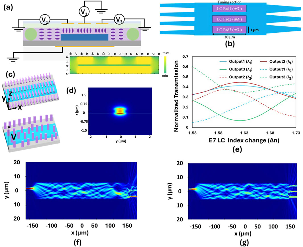
Figure 4. (a) Schematic cross-sectional view of the E7 LC-filled cell with voltage sources connected to the Au pads. The inset shows the corresponding electrostatic field profile. (b) The proposed programmable 4 × 3 MMI coupler showing the three pads in the tuning section. (c) Illustration of the LC director reorientation under an applied voltage. (d) Transverse magnetic mode profiles of the input waveguide. (e) Calculated normalized transmission variations for the three output waveguides as the refractive index of LC pad1 changes. Solid and dotted lines correspond to the source positions at the first and second input waveguides, respectively. (f,g) Optical field distribution in the 4 × 3 MMI coupler for two different refractive indices of the LC in the pad1 section.
4 Optical neural network modelling and simulation
Artificial neural networks (ANNs) process input data through interconnected layers of neurons or nodes. During training with a specific dataset, the network learns to execute designated tasks effectively by optimizing its parameters. Once trained, the ANN generalizes its learning to new datasets, achieving high-accuracy results. The model can then be used for inference, making predictions on unseen data based on the acquired knowledge. Figure 5a visually depicts the overall architecture of an ANN, highlighting the flow of input data through layers of neurons, including intermediary (hidden) layers, with the final classification outcome appearing at the output layer. Each neuron generates an output by applying a non-linear activation function to the weighted sum of its inputs, as shown in Figure 5a. In this study, we present a novel end-to-end integrated photonic neural network designed for rapid, sub-nanosecond classification tasks using computation by propagation. The architecture of the implemented integrated photonic neural network and the system configuration with the proposed programmable MMI coupler are illustrated in Figures 5b,c, respectively.
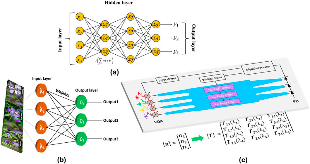
Figure 5. (a) A schematic illustration of a deep neural network, featuring the input layer, followed by multiple hidden layers, and an output layer that provides classification outputs. (b) The optical neural network architecture involves forming the input parameters of Iris flowers into a 120 × 4 dataset. This dataset is then directed to the first layer, where the input and output neurons is interconnected through a weighting system. (c) Schematic of a system architecture using programmable 4 × 3 MMI coupler, where the transmission matrix [T] is reconfigurable by modifying the refractive index of the tuning pads [n].
The dataset is encoded into the amplitude of distinct optical sources using a variable optical attenuator (VOA). These optical signals are then fed into the input waveguides of the programmable MMI, where they are processed as light propagates through the neurons (pads) within the MMI structure. By adjusting the local refractive index within the MMI, we can program the transmission matrix of the MMI for custom operation. To evaluate the proposed programmable MMI’s performance in classification tasks, we developed a neural network simulator in a co-simulation environment using both Lumerical and Python. This simulator supports neural network training for a defined number of epochs and performs inference operations. Two approaches were used for data processing at each epoch within the simulator:
1. Dynamic Refractive Index Update: In this method, the refractive index values of the LC regions are dynamically updated in Lumerical’s varFDTD solver for each epoch. This approach provides precise optical transmission data controlled by a PyTorch-based neural network model (co-simulation).
2. Discrete Refractive Index Levels: This method involves pre-defining discrete refractive index levels for each tuning pad. During training and inference, optical transmission is interpolated from a pre-simulated transmission dataset, created using a parameter sweep in Lumerical varFDTD. While the first method requires simulating the MMI structure at every epoch—resulting in longer training times—the second method, once the dataset is prepared, eliminates the need for repeated simulations. Although the interpolation method introduces minor errors, it offers faster training and inference times, making it the preferred approach for validating the device concept.
The simulator’s workflow for training and optimization is depicted in Figure 6. Initially, the refractive index values of each pad are set by applying voltages to the pads. Next, the optical transmission data is interpolated from the pre-generated dataset. The input dataset of the Iris image is encoded into the amplitude of optical sources at each input waveguide. The optical transmission at each output waveguide is then computed based on the input data and the refractive index values of the MMI coupler LC pads. From the resulting optical transmission, the loss and accuracy are evaluated. This process is iteratively performed over a specified number of epochs to train the neural network. To minimize loss at each epoch, the refractive index of the pads is optimized through gradient-based methods. The gradient is computed using finite differences by comparing the original loss with the loss obtained by incrementally adjusting the refractive index at each LC pad sequentially. Overall, the second approach enables efficient and rapid training of the neural network while maintaining a balance between accuracy and computational speed, demonstrating the potential of the proposed programmable MMI coupler in photonic neural network applications.
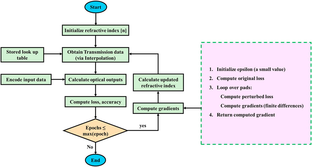
Figure 6. Flow diagram illustrating the training and optimization process of the proposed optical neural network, highlighting key steps such as refractive index initialization, optical transmission interpolation, loss calculation, and gradient-based optimization.
5 Results and analysis
To evaluate the performance of the proposed optical neural network (ONN) using a programmable MMI as a non-linear neuron, we conducted classification tasks using the Iris flower dataset. This dataset contains 150 samples, each with four input attributes and three output classes: “Virginia,” “Versicolor,” and “Setosa.” We divided the dataset into a training set and a test set with a 4:1 ratio. The classification process begins by encoding input values into optical signals and feeding them into the corresponding input waveguides of the MMI. During training, the optical transmission are optimized by changing the refractive indices of the LC tuning pads using an algorithm. Figures 7a,b show the evolution of the loss value and test accuracy over epochs. The confusion matrix for the test set is presented in Figure 7c, and Figure 7d shows the evolution of the transmission matrix parameters over training epochs, highlighting the dynamic optimization of optical synaptic weights in the MMI coupler. The gradual adjustments in transmission coefficients reflect the learning process, where the device adapts to achieve the desired computational functionality. The inset shows the variation of the refractive index during training, demonstrating the voltage-controlled tuning of LC elements to optimize light propagation and synaptic weighting. The proposed ONN achieves an accuracy of 86.67%, demonstrating its classification capability with just three pads and a single-layer system. The training process’s success depends on the initialization of pad indices and the learning rate, which influences optimization stability and speed. Figure 8a illustrates how different learning rates (0.01, 0.001, and 0.0001) affect loss and accuracy. Higher learning rates allow faster convergence, with fewer epochs needed to achieve maximum accuracy. We validated the interpolation method by comparing the simulator’s results with the co-simulation using FDTD data. Figure 8b demonstrates a strong correlation between the two approaches for a learning rate of 0.01, and with both methods achieving a consistent maximum accuracy of 86.67%. In comparison, a software-based neural network with the same architecture, implemented in PyTorch, achieved a higher accuracy of 93.3%. The maximum deviation in loss between the two methods was less than 0.8% (see inset of Figure 8b), and the average error was approximately 0.29%. This demonstrates that the interpolation method introduces only minimal error while significantly reducing the computational time required for training. The current ONN model has limitations due to its simple architecture, including a single layer and only three neurons (pads). Increasing the number of neurons, layers, or the discretization level of each pad could enhance accuracy. However, this would exponentially increase number of simulations, simulation time and training duration. This limitation can be mitigated when MMI devices are fabricated, allowing experimental data to streamline the training process. A unique characteristic of our ONN is how weights are updated collectively, with the 12-element weight matrix (transmission matrix) configured using only three refractive index parameters. Changes in any one pad affect all weight matrix elements, introducing complexity but also potentially reducing the parameter space by coupling weights. Although the weight matrix currently supports only non-negative values, this could be addressed using a balanced photodetector scheme or a second MMI to introduce negative weights. Additionally, coherent operations could enable complex matrix multiplications. These implementation options are further elaborated in the Supplementary Material (see Supplementary Note 1). The proposed ONN also benefits from its low power consumption. The LC-based optical phase shifter used in the MMI operates at nanowatt (∼nW) power levels (Xing et al., 2015; Alloat et al., 2012), which is significantly lower than conventional thermal phase shifters that typically consume power in the milliwatt (mW) range. For our MMI coupler with three pads, the power needed for a single multiply-accumulate (MAC) operation is estimated to be in the hundreds of nW. The overall energy consumption for the inference operation is in the femtojoule-per-operation range, highlighting the efficiency of the proposed design. Latency in the ONN is minimal, primarily governed by the propagation time of optical modes through the compact MMI structure, input loading time, and the response time of the photodetector. Consequently, the total latency is in the tens of picoseconds, making the ONN suitable for high-speed operations.
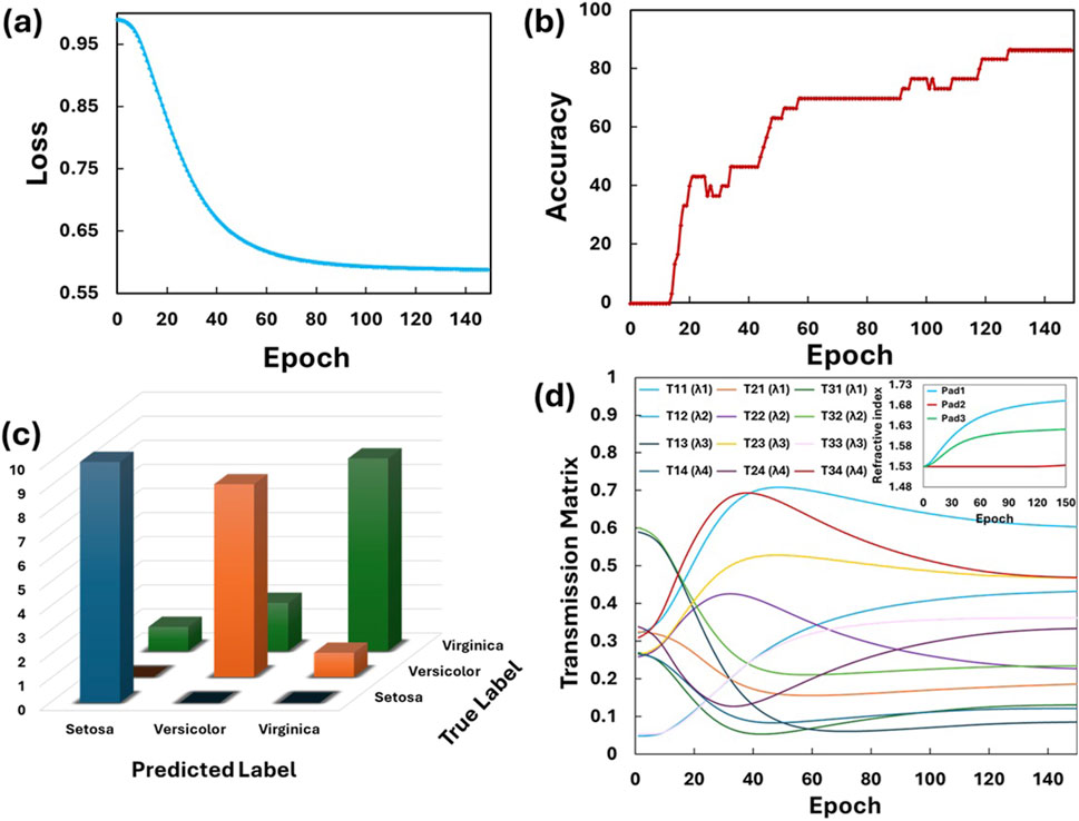
Figure 7. (a) The loss curve on the training set, (b) test accuracy curves and (c) the confusion matrix of the Iris image classification task using the proposed neural network. (d) Evolution of the transmission matrix parameters over training epochs, illustrating the dynamic adjustment of optical responses during optimization. The inset shows the variation of the refractive index throughout the training process, highlighting the adaptive tuning of the LC elements to achieve optimal performance.
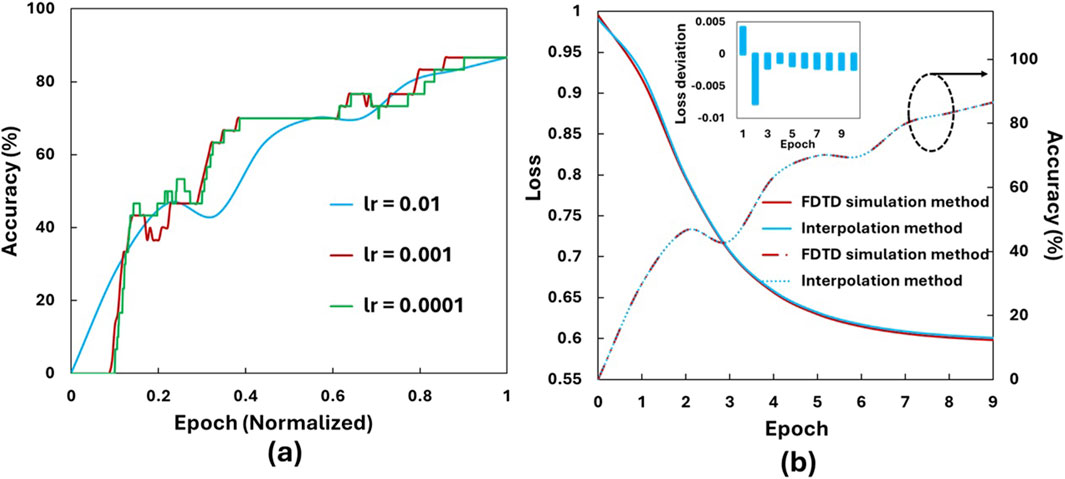
Figure 8. (a) The impact of different learning rate (lr) values on the accuracy curve. (b) Comparison of loss and test accuracy using both FDTD simulation and interpolation methods at a learning rate (lr) of 0.01. Inset: Error bars show the loss deviation between the FDTD simulation and interpolation methods at each epoch.
Table 1 provides a performance comparison of the proposed reconfigurable MMI coupler with previously reported reconfigurable and MMI-like structures. The comparison considers key parameters, including the device type, substrate material, reconfigurability, electro-optic (EO) mechanism, device footprint, and power consumption. The proposed 4 × 3 MMI coupler employs an indium phosphide (InP) membrane on a silicon (Si) substrate with an active electro-optic mechanism using E7 liquid crystal. It features a compact footprint of 285 μm × 11.5 μm and demonstrates extremely low power consumption in the nanowatt (nW) range. In comparison, previous devices exhibit varying performance characteristics. For instance, the unpatterned 4 × 4 MMI coupler on an InGaAsP substrate utilizes an active reconfiguration approach with a patterned pumping light mechanism, consuming an average pumping power of 1.5 mW (Wu et al., 2023). Another approach, utilizing two 4 × 4 MMI cells and microheater phase shifters on a SiN substrate, demonstrates a smaller footprint (275 μm × 15 μm) but higher energy consumption (4.84 pJ/MAC) (Meng et al., 2023). A particularly compact design, the 4 × 4 MMI coupler with a passive inverse design on a silicon substrate, achieves a footprint of only 4 μm × 4 μm but lacks reconfigurability. Similarly, several other passive designs, including the 10 × 10 and 14 × 10 MMI structures, do not offer reconfigurability, limiting their adaptability in dynamic applications. The proposed device’s key advantages lie in its reconfigurable nature, small footprint, and minimal power consumption. The use of a LC-based electro-optic mechanism enables dynamic control with low energy requirements, positioning this device as a promising candidate for scalable and power-efficient optical neural networks and other photonic computing applications.
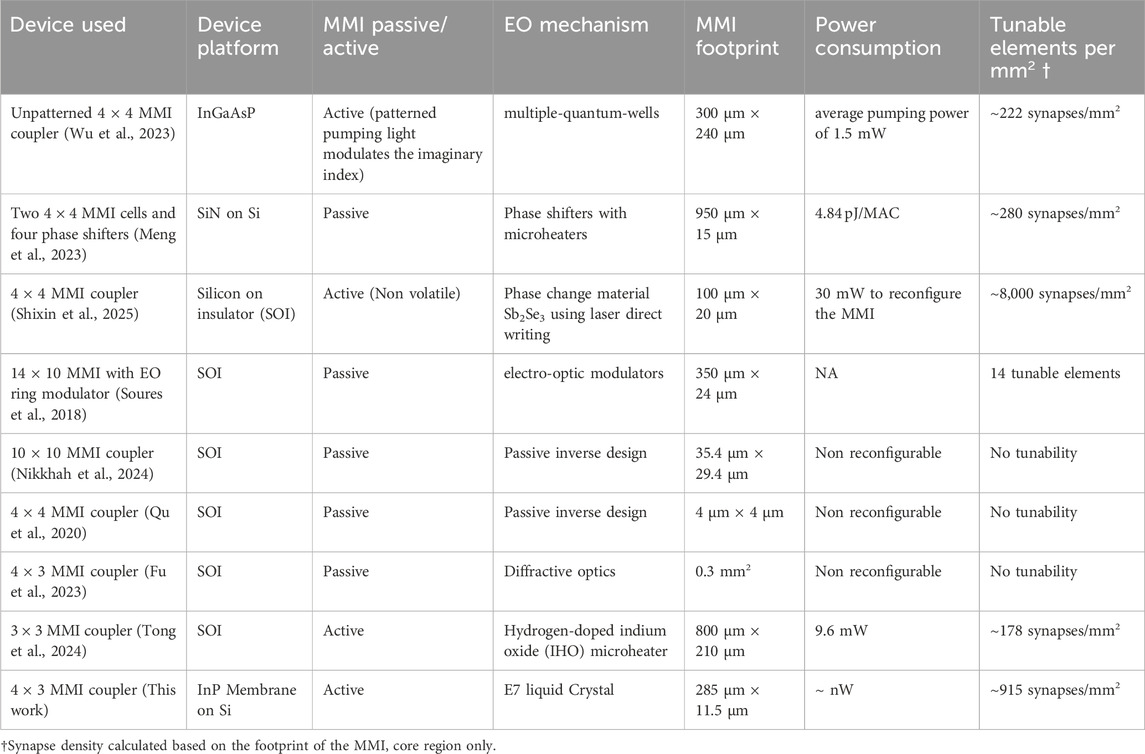
Table 1. Performance comparison of the proposed reconfigurable MMI coupler with previously reported reconfigurable MMI and MMI-like structures.
The current accuracy of 86.67% on the Iris dataset reflects a trade-off between simplicity of the hardware (i.e., a single-layer network with three tuning pads) and learning capacity. Increasing the number of control pads per MMI unit or cascading multiple MMI units to form deeper, multi-layer networks could significantly enhance classification performance. The scalability and potential extensions of the network are further discussed in Section 7.
To contextualize the novelty of our LC-MMI-based reconfigurable photonic neural network, we compare our approach with several state-of-the-art programmable photonic platforms used for neural inference. Supplementary Table S1 in the supplementary note 2 summarizes key metrics including inference accuracy, energy consumption, switching speed, and endurance. This helps situate our architecture within the field and demonstrates its advantages—such as ultra-low energy consumption, electrical tunability, and high reconfigurability—while also acknowledging areas for future development, particularly in improving tuning speed.
The LC reconfiguration time dictates the update rate of synaptic weights. The nematic E7 liquid crystal used in this study typically exhibits switching times on the order of milliseconds. Although this response is slower than other tuning mechanisms, such as thermo-optic or electro-optic effects, it remains suitable for applications where weight updates are infrequent or where inference operations dominate. To enable faster reconfiguration in future implementations, alternative materials—such as ferroelectric liquid crystals or polymer-stabilized LCs—could be considered, as they offer significantly faster response times, often in the microsecond or sub-microsecond range.
6 Device fabrication
This section outlines a potential fabrication process for the proposed LC-based reconfigurable optical device, which features a programmable multimode interference (MMI) coupler on an indium phosphide (InP) membrane. The InP membrane platform is selected due to its high refractive index contrast, which allows for the miniaturization of photonic components, as well as its compatibility with active photonic devices. These characteristics make it particularly suitable for reconfigurable optical neural network applications (Jiao et al., 2020b). The detailed process flow is illustrated in Figure 9. The initial InP epi-wafer is grown using metalorganic vapor phase epitaxy (MOVPE) and consists of a layer stack of 50 nm i-InP, 50 nm i-InGaAs, 300 nm i-InP, 300 nm i-InGaAs, and an InP substrate. As the first step of the fabrication process, the 50 nm i-InP and 50 nm i-InGaAs cap layers are removed by wet etching, as illustrated in Figure 9a. Following this, a polyimide (PI) layer is spin-coated onto the InP wafer, followed by curing to form a uniform cladding layer. Next, Ti/Au metal electrodes are deposited and patterned to create metal pads, as shown in Figure 9b. To improve adhesion, thin SiO2 layers are deposited via plasma-enhanced chemical vapor deposition (PECVD) on both the InP and Si wafers (not shown in Figure 9). A benzocyclobutene (BCB) layer is then spin-coated onto the InP wafer, serving as the adhesive bonding layer, as depicted in Figure 9c. The wafer bonding process is performed in a vacuum environment to ensure high-quality adhesion and minimize void formation. Following bonding, the InP substrate and the InGaAs etch-stop layer are selectively removed using wet etching. The photonic structures on the InP membrane are then defined through electron beam lithography (EBL) and reactive ion etching (RIE), as illustrated in Figure 9d. An additional PI layer is spin-coated, patterned via UV exposure with a mask, developed, and cured to create the separation layer for the LC cell. A glass wafer with pre-patterned Au/Ti electrodes (pre-coated with an LC alignment layer to facilitate uniform molecular orientation, not shown in Figure 9) is then bonded to the patterned PI top cladding using a UV-curable adhesive, forming empty cells for LC alignment (Figure 9e). The final step involves filling the empty cells with E7 LC through capillary action (Figure 9f).
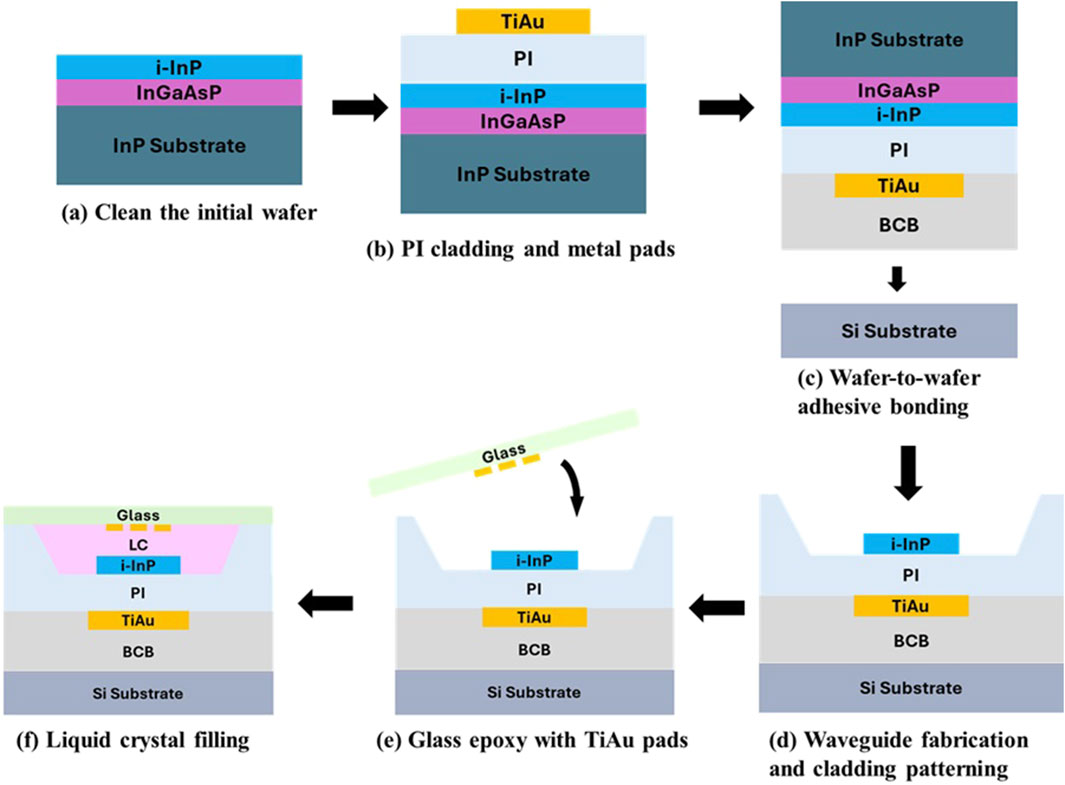
Figure 9. Schematic diagram illustrating the step-by-step fabrication process of the proposed LC-based reconfigurable optical device. (a) Clean the initial InP-based wafer stack, (b) deposit the PI cladding layer and form Ti/Au metal pads, (c) perform wafer-to-wafer adhesive bonding with a silicon substrate using BCB, (d) define the waveguide structure and pattern the cladding layers, (e) bond a glass substrate with epoxy over the cladding, and (f) fill the cavity with liquid crystal (LC) material.
7 Scalability, multi-layer integration, and associated challenges
The current implementation of the programmable MMI-based synaptic weighting engine, utilizing three independently tunable LC pads, serves as a proof-of-concept for demonstrating the feasibility of reconfigurable, low-power photonic neural elements. However, practical neuromorphic systems will require scalability in both functional complexity and physical design.
The number of control pads can be increased along the MMI region to allow more fine-grained control over the interference pattern and thereby enable higher-resolution synaptic weighting. However, careful design is required to avoid cross-talk between electrodes and to maintain uniform LC alignment. From a fabrication standpoint, photolithographic definition of additional electrodes is feasible. Modeling complexity indeed increases as the number of control pads grows. Specifically, the total number of required simulations to fully characterize the system scales as NM, where N is the number of discrete voltage levels per pad and M is the number of control pads. For instance, with 3 pads and 9 discrete voltage levels, the system provides 729 possible synaptic states. Increasing the number of pads to 5, while maintaining the same voltage resolution, would yield 32,768 states, significantly enhancing the granularity of optical weighting. This exponential growth poses computational challenges. However, this can be managed through efficient interpolation schemes, surrogate modeling, or by leveraging parallelized optimization and simulation pipelines. In our current implementation, we have already employed an interpolation-based method to significantly reduce simulation overhead, and we envision similar strategies being applied to larger-scale systems. Nonetheless, higher pad counts introduce additional considerations, such as inter-electrode crosstalk, increased design complexity, and expanded control parameter spaces during training.
For extending to multilayer neural networks, multiple MMI units can be cascaded or interconnected using integrated waveguide routing. Each stage could represent a linear matrix operation followed by a nonlinear activation, mimicking the structure of traditional deep learning architectures. This modular design enables flexible and scalable implementations of deeper photonic neural networks. One of the key challenges in such multi-layer systems is optical loss accumulation. Here, our choice of the InP platform offers a distinct advantage—active components such as semiconductor optical amplifiers (SOAs) or integrated laser sources can be co-fabricated to provide on-chip gain, mitigating interconnect losses and enabling signal regeneration between layers. Additional considerations such as signal synchronization, phase stability, and thermal effects are being actively explored in our ongoing work.
By increasing the number of input/output ports and integrating additional tuning pads, the MMI can accommodate larger matrix-vector multiplications, allowing the system to process more features per layer (Bolk et al., 2018). This enhancement allows the system to process higher-dimensional inputs, such as those in datasets like MNIST, and expands the network’s capacity per layer.
While the proposed LC-MMI architecture demonstrates effective reconfigurability for optical neural network applications, practical integration challenges must also be addressed to ensure robust and scalable operation. Maintaining uniform LC alignment across the MMI region is essential for consistent refractive index modulation. In our current design, alignment is achieved using standard surface treatment techniques, such as rubbed polyimide layers or photoalignment using polarized UV light. These methods have been widely adopted in display and LC-integrated optical systems and provide repeatable and scalable alignment across planar photonic platforms. The long-term operational stability of the LC layer is influenced by factors such as encapsulation quality and potential material degradation under optical and thermal stress. To address this, we encapsulate the LC using inert top cladding materials, such as glass or polymeric layers, that prevent contamination and evaporation. Moreover, LCs used in our study (e.g., E7-type nematic LCs) are known to exhibit stable electro-optic properties over extended durations under moderate voltage and temperature conditions (Woods et al., 2018; Brugioni et al., 2003). The thermo-optic response of LCs introduces a dependence of the refractive index on ambient temperature (Li et al., 2005). While this could potentially affect the consistency of weight tuning, the temperature-induced index change for nematic LCs is relatively small within a standard operating window (20°C–40°C). In our architecture, such variations can be compensated through voltage adjustments to the control pads. For high-precision or thermally variable environments, future implementations could include temperature feedback loops or explore more thermally stable LC formulations. Additionally, based on prior experience, the nematic phase range can be broadened by formulating custom LC blends, enabling more stable operation across wider temperature ranges. As the number of control pads increases, minimizing electrical and optical crosstalk becomes essential. This can be managed through careful electrode layout, shielding strategies, and appropriate spacing of LC regions to ensure field confinement. Beyond physical mitigation, training-aware methods can help compensate for residual interference. Since weights do not need to be fully uncorrelated, the network can learn robust configurations that tolerate moderate crosstalk during training. MMI devices are inherently robust to small dimensional variations, which is a key advantage over more sensitive interferometric meshes. Nonetheless, consistent LC layer thickness and uniform alignment are critical. Our fabrication process uses standard lithographic and alignment techniques, which are scalable and reproducible.
8 Conclusion
This paper presents a novel reconfigurable feedforward neural network architecture implemented on an InP membrane platform, leveraging the electro-optic properties of LC to dynamically program the transmission matrix of a MMI coupler. The proposed design enables compact, programmable optical weighting and demonstrates effective classification performance on the Iris dataset using a hybrid co-simulation framework. While the architecture offers a reduced footprint and fewer control pads compared to other photonic neural networks, it is currently limited to a single-layer configuration, which restricts its ability to model more complex learning tasks. Additionally, although inference latency is extremely low due to passive optical propagation, the LC tuning speed remains relatively slow, which may limit the frequency of reconfiguration in dynamic applications. Future work will explore multi-layer implementations using cascaded MMI networks, as well as the integration of faster electro-optic materials such as ferroelectric liquid crystals. The approach also holds promise for scaling to more complex datasets and larger neural network models, paving the way toward practical, high-speed, and reconfigurable photonic computing systems.
Data availability statement
The original contributions presented in the study are included in the article/Supplementary Material, further inquiries can be directed to the corresponding author.
Author contributions
RG: Software, Methodology, Writing – review and editing, Investigation, Writing – original draft, Validation, Resources, Data curation, Visualization, Formal Analysis, Conceptualization, Project administration. DL: Formal Analysis, Validation, Writing – review and editing, Resources, Conceptualization, Funding acquisition, Supervision. SR: Validation, Writing – review and editing, Investigation. YJ: Writing – review and editing, Investigation, Validation, Resources. WY: Resources, Conceptualization, Project administration, Methodology, Writing – review and editing, Supervision, Funding acquisition.
Funding
The author(s) declare that financial support was received for the research and/or publication of this article. This work is partially funded by the EIC SPIKEPro project under grant agreement 101129904 and the Eindhoven Hendrik Casimir Institute.
Acknowledgments
Portions of this work were previously presented at the International Photonic Conference (IPC), Rome, Italy, in 2024 (DOI: 10.1109/IPC60965.2024.10799915).
Conflict of interest
The authors declare that the research was conducted in the absence of any commercial or financial relationships that could be construed as a potential conflict of interest.
Generative AI statement
The author(s) declare that no Generative AI was used in the creation of this manuscript.
Publisher’s note
All claims expressed in this article are solely those of the authors and do not necessarily represent those of their affiliated organizations, or those of the publisher, the editors and the reviewers. Any product that may be evaluated in this article, or claim that may be made by its manufacturer, is not guaranteed or endorsed by the publisher.
Supplementary material
The Supplementary Material for this article can be found online at: https://www.frontiersin.org/articles/10.3389/fnano.2025.1593347/full#supplementary-material
References
Alloatti, L., Pfeifle, J., Mendez, J., Freude, W., Leuthold, J., and Koos, C. (2012). “Liquid crystal phase shifter on the SOH platform with ultra-low power consumption,” Optical Fiber Communication Conference (Washington: DC: Optica Publishing Group), OTu1I–5.
Bachmann, M., Besse, P. A., and Melchior, H. (1995). Overlapping-image multimode interference couplers with a reduced number of self-images for uniform and nonuniform power splitting. Appl. Opt. 34, 6898–6910. doi:10.1364/AO.34.006898
Bai, Y., Xu, X., Tan, M., Sun, Y., Li, Y., Wu, J., et al. (2023). Photonic multiplexing techniques for neuromorphic computing. Nanophotonics 12, 795–817. doi:10.1515/nanoph-2022-0485
Basu, R., and Shalov, S. A. (2017). Graphene as transmissive electrodes and aligning layers for liquid-crystal-based electro-optic devices. Phys. Rev. E 96, 012702. doi:10.1103/PhysRevE.96.012702
Bolk, J., Ambrosius, H., Stabile, R., Latkowski, S., Leijtens, X., Bitincka, E., et al. (2018). Deep UV lithography process in generic InP integration for arrayed waveguide gratings. IEEE Photonics Technol. Lett. 30, 1222–1225. doi:10.1109/LPT.2018.2840224
Brugioni, S., Faetti, S., and Meucci, R. (2003). Mid-infrared refractive indices of the nematic mixture E7. Liq. Cryst. 30, 927–930. doi:10.1080/0267829031000136057
Cheng, Z., Ríos, C., Pernice, W. H., Wright, C. D., and Bhaskaran, H. (2017). On-chip photonic synapse. Sci. Adv. 3, 1700160. doi:10.1126/sciadv.1700160
Dabos, G., Bellas, D. V., Stabile, R., Moralis-Pegios, M., Giamougiannis, G., Tsakyridis, A., et al. (2022). Neuromorphic photonic technologies and architectures: scaling opportunities and performance frontiers [Invited]. Opt. Mater. Express 12, 2343–2367. doi:10.1364/OME.452138
Feldmann, J., Youngblood, N., Karpov, M., Gehring, H., Li, X., Stappers, M., et al. (2021). Parallel convolutional processing using an integrated photonic tensor core. Nature 589, 52–58. doi:10.1038/s41586-021-03216-9
Ferreira de Lima, T., Shastri, B. J., Tait, A. N., Nahmias, M. A., and Prucnal, P. R. (2017). Progress in neuromorphic photonics. Nanophotonics 6, 577–599. doi:10.1515/nanoph-2016-0139
Fu, T., Zang, Y., Huang, Y., Du, Z., Huang, H., Hu, C., et al. (2023). Photonic machine learning with on-chip diffractive optics. Nat. Commun. 14, 70. doi:10.1038/s41467-022-35772-7
Fukuhara, K., Nagano, S., Hara, M., and Seki, T. (2014). Free-surface molecular command systems for photoalignment of liquid crystalline materials. Nat. Commun. 5, 3320. doi:10.1038/ncomms4320
Giamougiannis, G., Tsakyridis, A., Mourgias-Alexandris, G., Moralis-Pegios, M., Totovic, A., Dabos, G., et al. (2021). “Silicon-integrated coherent neurons with 32GMAC/sec/axon compute line-rates using EAM-based input and weighting cells,” in 2021 European conference on optical communication (ECOC) (IEEE), 1–4. doi:10.1109/ECOC52684.2021.9605987
Guo, X., Xiang, J., Zhang, Y., and Su, Y. (2021). Integrated neuromorphic photonics: synapses, neurons, and neural networks. Adv. Photonics Res. 2, 2000212. doi:10.1002/adpr.202000212
Jiao, Y., Nishiyama, N., Van Der Tol, J., Van Engelen, J., Pogoretskiy, V., Reniers, S., et al. (2020a). InP membrane integrated photonics research. Semicond. Sci. Technol. 36, 013001. doi:10.1088/1361-6641/abcadd
Jiao, Y., van der Tol, J., Pogoretskii, V., van Engelen, J., Kashi, A. A., Reniers, S., et al. (2020b). Indium phosphide membrane nanophotonic integrated circuits on silicon. Phys. status solidi (a) 217, 900606. doi:10.1002/pssa.201900606
Jouppi, N. P., Young, C., Patil, N., Patterson, D., Agrawal, G., Bajwa, R., et al. (2017). “In-datacenter performance analysis of a tensor processing unit,” in Proceedings of the 44th annual international symposium on computer architecture, 1–12.
Lee, S. L., Mao, C. N., and Lin, Y. H. (2023). Investigation of a polarizer-free liquid crystal phase modulation via nanometer size encapsulation of nematic liquid crystals. Opt. Mater. Express 13, 3531–3542. doi:10.1364/OME.509266
Leuthold, J., and Joyner, C. H. (2001). Multimode interference couplers with tunable power splitting ratios. J. Light. Technol. 19, 700–707. doi:10.1109/50.923483
Li, J., Wu, S. T., Brugioni, S., Meucci, R., and Faetti, S. (2005). Infrared refractive indices of liquid crystals. J. Appl. Phys. 97, 97. doi:10.1063/1.1877815
Liao, K., Dai, T., Yan, Q., Hu, X., and Gong, Q. (2023). Integrated photonic neural networks: opportunities and challenges. ACS Photonics 10, 2001–2010. doi:10.1021/acsphotonics.2c01516
Liu, D., and Broer, D. J. (2014). Liquid crystal polymer networks: preparation, properties, and applications of films with patterned molecular alignment. Langmuir 30, 13499–13509. doi:10.1021/la500454d
Meng, X., Zhang, G., Shi, N., Li, G., Azaña, J., Capmany, J., et al. (2023). Compact optical convolution processing unit based on multimode interference. Nat. Commun. 14, 3000. doi:10.1038/s41467-023-38786-x
Miscuglio, M., and Sorger, V. J. (2020). Photonic tensor cores for machine learning. Appl. Phys. Rev. 7, 7. doi:10.1063/5.0001942
Nahmias, M. A., Peng, H. T., De Lima, T. F., Huang, C., Tait, A. N., Shastri, B. J., et al. (2018). “A TeraMAC neuromorphic photonic processor,” in 2018 IEEE photonics conference (IPC) (IEEE), 1–2. doi:10.1109/IPCon.2018.8527089
Nikkhah, V., Pirmoradi, A., Ashtiani, F., Edwards, B., Aflatouni, F., and Engheta, N. (2024). Inverse-designed low-index-contrast structures on a silicon photonics platform for vector–matrix multiplication. Nat. Photonics 18, 501–508. doi:10.1038/s41566-024-01394-2
Peruzzo, A., Laing, A., Politi, A., Rudolph, T., and O'brien, J. L. (2011). Multimode quantum interference of photons in multiport integrated devices. Nat. Commun. 2, 224. doi:10.1038/ncomms1228
Qu, Y., Zhu, H., Shen, Y., Zhang, J., Tao, C., Ghosh, P., et al. (2020). Inverse design of an integrated-nanophotonics optical neural network. Sci. Bull. 65, 1177–1183. doi:10.1016/j.scib.2020.03.042
Samoi, E., Benezra, Y., and Malka, D. (2020). An ultracompact 3× 1 MMI power-combiner based on Si slot-waveguide structures. Photonics Nanostructures-Fundamentals Appl. 39, 100780. doi:10.1016/j.photonics.2020.100780
Shastri, B. J., Tait, A. N., Ferreira de Lima, T., Pernice, W. H., Bhaskaran, H., Wright, C. D., et al. (2021). Photonics for artificial intelligence and neuromorphic computing. Nat. Photonics 15, 102–114. doi:10.1038/s41566-020-00754-y
Shen, Y., Harris, N. C., Skirlo, S., Prabhu, M., Baehr-Jones, T., Hochberg, M., et al. (2017). Deep learning with coherent nanophotonic circuits. Nat. photonics 11, 441–446. doi:10.1038/nphoton.2017.93
Shi, B., Calabretta, N., and Stabile, R. (2019). Deep neural network through an InP SOA-based photonic integrated cross-connect. IEEE J. Sel. Top. Quantum Electron. 26, 1–11. doi:10.1109/JSTQE.2019.2945548
Shixin, G., Haonan, R., Jingzhe, P., Yang, R., Zhenqing, Z., Shuang, Z., et al. (2025). Reconfigurable free form silicon photonics by phase change waveguides. Adv. Opt. Mater. 13, 2402997. doi:10.1002/adom.202402997
Soldano, L. B., and Pennings, E. C. (1995). Optical multi-mode interference devices based on self-imaging: principles and applications. J. Light. Technol. 13, 615–627. doi:10.1109/50.372474
Soures, N., Steidle, J., Preble, S., Kudithipudi, D., and Neuro-MMI, (2018). “A hybrid photonic-electronic machine learning platform,” in 2018 IEEE photonics society summer topical meeting series (SUM), 187–188. doi:10.1109/PHOSST.2018.8456766
Sze, V., Chen, Y. H., Emer, J., Suleiman, A., and Zhang, Z. (2017). “Hardware for machine learning: challenges and opportunities,” in IEEE custom integrated circuits conference (CICC), 1–8.
Tahersima, M. H., Kojima, K., Koike-Akino, T., Jha, D., Wang, B., Lin, C., et al. (2019). Deep neural network inverse design of integrated photonic power splitters. Sci. Rep. 9, 1368. doi:10.1038/s41598-018-37952-2
Tait, A. N., De Lima, T. F., Zhou, E., Wu, A. X., Nahmias, M. A., Shastri, B. J., et al. (2017). Neuromorphic photonic networks using silicon photonic weight banks. Sci. Rep. 7, 7430. doi:10.1038/s41598-017-07754-z
Tong, W., Yang, E., Dong, J., Hu, B., and Zhang, X. (2024). IHO film microheater-assisted planar waveguide photonic emulator. J. Light. Technol. 42, 8269–8274. doi:10.1109/JLT.2024.3433573
Von Bieren, K. (1971). Lens design for optical Fourier transform systems. Appl. Opt. 10, 2739–2742. doi:10.1364/AO.10.002739
Woods, V., Trumpis, M., Bent, B., Palopoli-Trojani, K., Chiang, C. H., Wang, C., et al. (2018). Long-term recording reliability of liquid crystal polymer µECoG arrays. J. neural Eng. 15, 066024. doi:10.1088/1741-2552/aae39d
Wu, T., Menarini, M., Gao, Z., and Feng, L. (2023). Lithography-free reconfigurable integrated photonic processor. Nat. Photonics 17, 710–716. doi:10.1038/s41566-023-01205-0
Xing, Y., Ako, T., George, J. P., Korn, D., Yu, H., Verheyen, P., et al. (2015). Digitally controlled phase shifter using an SOI slot waveguide with liquid crystal infiltration. IEEE Photonics Technol. Lett. 27, 1269–1272. doi:10.1109/LPT.2015.2416438
Xu, X., Tan, M., Corcoran, B., Wu, J., Boes, A., Nguyen, T. G., et al. (2021). 11 TOPS photonic convolutional accelerator for optical neural networks. Nature 589, 44–51. doi:10.1038/s41586-020-03063-0
Zhang, H., Gu, M., Jiang, X. D., Thompson, J., Cai, H., Paesani, S., et al. (2021). An optical neural chip for implementing complex-valued neural network. Nat. Commun. 12, 457. doi:10.1038/s41467-020-20719-7
Zhou, H., Dong, J., Cheng, J., Dong, W., Huang, C., Shen, Y., et al. (2022). Photonic matrix multiplication lights up photonic accelerator and beyond. Light Sci. and Appl. 11, 30. doi:10.1038/s41377-022-00717-8
Keywords: photonic integrated circuits, programmable photonics, multimode interference, InP photonics, liquid crystal, optical neural network
Citation: Ghosh RR, Liu D, Reniers S, Jiao Y and Yao W (2025) Reconfigurable optical synaptic weighting engine using a liquid crystal-based multimode interference coupler. Front. Nanotechnol. 7:1593347. doi: 10.3389/fnano.2025.1593347
Received: 13 March 2025; Accepted: 18 June 2025;
Published: 18 July 2025.
Edited by:
Bin Shi, Hewlett Packard Enterprise, United StatesReviewed by:
Arindam Dasgupta, University of Central Florida, United StatesErick Ulin-Avila, Arkansas State University, United States
Copyright © 2025 Ghosh, Liu, Reniers, Jiao and Yao. This is an open-access article distributed under the terms of the Creative Commons Attribution License (CC BY). The use, distribution or reproduction in other forums is permitted, provided the original author(s) and the copyright owner(s) are credited and that the original publication in this journal is cited, in accordance with accepted academic practice. No use, distribution or reproduction is permitted which does not comply with these terms.
*Correspondence: Rajib Ratan Ghosh, ci5yLmdob3NoQHR1ZS5ubA==