 Yoosuk Kim
 Irma Kuljanishvili
- Department of Physics, Saint Louis University, St. Louis, MO, United States
Carbon nanotubes (CNTs) have gained significant attention in the scientific and technology sectors due to their exceptional physical, chemical, and electronic properties. These qualities make them excellent candidates for several electronic applications, such as ballistic conduction, high current densities, low power consumption, outstanding single-photon capacity, and excellent nano-mechanical resonators. However, incorporating CNTs into specific micro- and nano-architectures and hybrid structures remains challenging. Developing fabrication and patterning technologies, involving CNTs, that can scale up while utilizing their exceptional properties has received significant attention in the last two decades. Various approaches have been investigated, including top-down and bottom-up methods, and new techniques have been used to achieve selective CNTs production through patterning. The continued developments of patterning technologies is critical for fully exploiting CNTs’ practical applicability. This mini-review looks at recent advances in fabrication and patterning of CNTs with micro- and nanoscale resolution, such as using pre-patterned substrates, dielectrophoresis, oxidative etching, and selective production and growth for CNTs, or direct printing of CNT-containing inks, etc. Article discusses advantages and limitations of various approaches for achieving accurate and scalable CNT patterning. Overcoming fabrication challenges will pave the way for a widespread use of CNTs in various applications including electronics, photonics, mechanical and biomedical devices and hybrid systems, etc.
1 Introduction
First discovered by Sumio Iijima in 1991, carbon nanotubes (CNTs) quickly gained interest in the scientific community due to their outstanding properties (Iijima, 1991). Carbon allotropes that include graphite, diamond, and fullerene, have remarkable mechanical, electrical, optical, and chemical properties (Kroto et al., 1985; Saito and Dresselhaus, 1998; Kataura et al., 1999; Dai, 2002b; Novoselov, 2009; Zhou et al., 2009; Aqel et al., 2012; Ibrahim, 2013; Zheng, 2017), yet carbon nanotubes possess special uniqueness as they have been long thought as possible building block as interconnects and/or active elements of electronic devices. Randomly assembled CNTs, however, exhibit lower electrical conductivity, negatively affecting device and system performance.
Patterning of CNTs is essential for designing and engineering new devices and hybrid systems with improved functionalities. In other words, precision and control in the way CNTs are designed and fabricated largely depends on methods that are used for patterning. CNT patterning introduces new possibilities for high-performance electronics, energy storage systems, sensitive sensors, and other novel applications (Hong et al., 2010; Hu et al., 2010; Volder et al., 2010; Chen et al., 2011). In patterned aligned CNTs, for example, electrons can move along more efficiently, which improves the electrical conductivity and performance of field effect transistors (FETs) (Javey et al., 2004; Patil et al., 2009a; Patil et al., 2009b; Freer et al., 2010; Ono et al., 2010; Chandra et al., 2011). In addition, combining CNTs with various semiconductors, nanoparticles, and polymers can improve the thermal, mechanical, and electrical properties of CNTs to create new types of heterostructured materials and hybrid devices. (Whitsitt and Barron, 2003; Fan et al., 2010; Dong et al., 2011; Liang et al., 2012; Cao et al., 2013; Chinnappan et al., 2016; Wu et al., 2017; Hameed et al., 2019).
Nevertheless, maintaining control over precise patterning at the micro- and nanometer scale continues to be challenging. Thin-film transistors, transparent conductive films, wearable devices, human-machine interfaces, medical applications, and flexible displays require precise placement of CNTs. Well-developed patterning methodologies can improve power densities, sizes, costs, and efficiencies of the fabrication process. Various techniques, including pre-patterned CNT growth catalysts, oxidative etching of CNT networks, and patterning using pre-dispersed CNT solutions, have been explored in recent past. In the following sections of the discussion, those techniques will be categories as bottom-up vs. top-down with subsequent analyses of their advantages and limitations.
1.1 Types and structures of CNTs
CNTs are classified into three types: single-wall CNT (SWCNT), double-wall CNT (DWCNT), and multi-wall CNT (MWCNT) (Iijima and Ichihashi, 1993; Zhao et al., 1997; Dai, 2002a; Aqel et al., 2012; Moore et al., 2015). SWCNTs consist of a single layer of graphene and form a seamless cylinder with electronic properties based on a chiral vector. Chiral vectors determine whether SWCNTs are metallic or semiconducting (Hodge et al., 2012; Tîlmaciu and Morris, 2015). The band gap of a semiconducting SWCNTs is inversely proportional to its diameter, smaller the diameter of the tube, larger the band-gap (Kataura et al., 1999; Wu et al., 2004; Dresselhaus et al., 2005; Turaeva et al., 2023). MWCNTs have multiple concentric layers of graphene cylinders, forming an overlapping tube-in-tube structure, and are predominately metallic.
The electrical properties of CNTs depend on factors such as chirality, diameter, length, and defect density. Metallic SWCNTs have high electrical conductivity, while semiconducting SWCNTs have lower conductivity, at room temperature (Tans et al., 1998; White and Todorov, 1998; Kociak et al., 2001). In CNTs, with low defect density electrons travel ballistically due to one-dimensional (1D) confinement, thus making them good candidates for high-electron-mobility devices (Liang et al., 2001) CNTs also have quantized energy levels and conductance (Odom et al., 2000; Javey et al., 2004). New methods for controlled synthesis and integration of CNTs into devices continues to drive ongoing research into many technological areas.
1.2 Synthesis and fabrication of CNTs
There are several ways to manufacture CNTs, each with benefits and drawbacks. In the first method, arc discharge, two graphite electrodes are used to form a plasma arc, in an inert gas atmosphere, (Iijima, 1991; Zhao et al., 1997). This method produces predominately MWCNTs and offers reasonably high production yields but generates impurities. Another method, laser ablation, involves irradiating a carbon target with a transition metal catalyst using a powerful laser beam (Guo et al., 1995; Arepalli, 2004). This allows for more precise control over the CNT diameter and chirality, leading to superior SWCNTs. However, low yield and scalability challenges affect large-scale production.
Chemical vapor deposition (CVD) is a method of choice when a more precise control over the growth condition, and resulting CNTs, is needed. (Baker, 1989; José-Yacamán et al., 1995; Li et al., 1996; Volder et al., 2013). There are a few different ways to implement this scalable technique. These include thermal CVD, plasma-enhanced CVD, and hot filament CVD (Wang et al., 2002; Meyyappan et al., 2003; Li et al., 2004; Kumar and Ando, 2010). In CVD synthesis transition metal catalysts are used to crack a hydrocarbon gas. CNTs generally grow via Vapor-Liquid-Solid (VLS) growth mechanism, with carbon atoms adsorbed onto the catalyst (Baker et al., 1973; Gavillet et al., 2001). Controlling the process parameters allows researchers to tune the diameter, chirality, and alignment of CNTs, via careful selection of catalysts, substrate, and environment (such as temperature, or pressure, etc.) (Turaeva and Kuljanishvili, 2021). Overall CVD enables a route for scalable and selective growth of high quality SWCNTs and MWCNTs. While much progress has been made in this area, the production of defect-free SWCNTs with high yields, desirable chirality, continues to be challenging. Therefore, when CNTs with targeted properties are desired, post-growth sorting and processing is often needed.
2 Micro- and nanoscale patterning of CNTs
Controlling the arrangement and orientation of CNTs is critical for their successful implementation in various device applications. There are two basic patterning categories: top-down and bottom-up. Briefly, the bottom-up methods in most cases involve metal catalysts and substrate. The CNTs are then grown on the substrate using a process, such as CVD. The growth process can be controlled to produce CNTs with specific dimensions and orientations. The top-down methods starts with CNTs dispersed in a solution such as solvent or polymer matrix. The solution is then deposited onto the substrate, and the CNTs are assembled into the desired pattern using either self-assembly or dielectrophoresis (DEPs). The choice of patterning method depends on the desired properties of the CNT-arrays. Patterning of CNTs can be a complex and challenging process, however, new approaches are continuously being developed. Some of the most common patterning methods are described below.
2.1 Bottom-up
Bottom-up approach has shown capacity for creating sub-micron resolution patterns. Usually, the patterning process occurs prior to the CNT growth, achieved through CVD synthesis. Growth catalysts, typically transition metal nanoparticles, are used to create specific patterns. However, temperatures (∼600°C–900°C) required during CNT synthesis limits substrates. Despite this limitation, bottom-up patterning approaches remain advantageous because they can create high-density CNT patterns and control selectivity and organization of the CNTs with respect to the substrate.
2.1.1 Catalyst lithographic patterning for the CNTs growth
Patterned catalysts can be prepared via photolithography, electron beam lithography (EBL), and focused ion beam lithography (FIBL), and subsequently produce CNTs during the growth. (Ishida et al., 2004; Imaizumi et al., 2005; Häffner et al., 2008; Liang et al., 2019). In recent studies, efforts have been made to overcome the disadvantages of these conventional lithographic processes. As shown in Figure 1A, catalytic photolithography is one of the most traditional methods for growing CNT forests by combining conventional catalyst deposition with catalytic etching. (Ahn et al., 2019). This technique allowed precise spatial control over the surface properties and selective deposition of catalyst precursors (Tawfick et al., 2010).
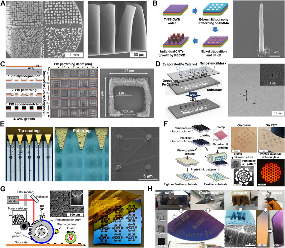
FIGURE 1. Bottom-up methods of patterning catalyst precursor for CNTs production. (A) MWCNT forests with various structures grown by pre-catalytic patterning with photolithography technology (Ahn et al., 2019) (Copyright 2019; Springer). (B) Individual MWCNTs grown on catalyst deposited on substrates by EBL (Jung and Lee, 2014) (Copyright 2014; Hindawi). (C) CNTs ensembles morphology according to the depth of catalytic patterning using FIB (Pander et al., 2017) (Copyright 2017; Springer). (D) Individual CNTs grown on catalyst islands deposited with a stencil shadow mask (Choi et al., 2013) (Copyright 2013; Springer). (E) Individually grown SWCNTs with catalytic ink written on pre-defined area by an AFM probe (Kuljanishvili et al., 2009) (Copyright 2009; Wiley-VCH). (F) Direct printing of ultrathin colloidal ink patterns using microstructured nanoporous stamps (Kim et al., 2016b) (Copyright 2016; Science). (G) Modified laser printing for large area fabrication of MWCNT forests micropatterns using catalytic nanoparticle toners (Polsen et al., 2013) (Copyright 2013; American Chemical Society). (H) DWCNT bundles patterned by inkjet printing, rubber stamping, spray coating, and fountain pen writing (King et al., 2020) (Copyright 2020; American Chemical Society).
As shown in Figure 1B, EBL allows the creation of catalyst patterns on substrates with nanometer precision (Jung and Lee, 2014). Therefore, isolated individual CNTs can grow selectively at precise locations (Liang et al., 2019). In another study, EBL can modify the growth substrate to immobilize the catalyst in the modified area (Carpena-Núñez et al., 2018). Patterned c-cut sapphire substrates were used irradiated by EBL, increasing surface roughness in the irradiated area. This method prevents Ostwald ripening of metal-catalyzed nanoparticles, thus enabling precise CNT forests formation during the growth.
FIBL is another precise lithographic technique used for nanoscale patterning. It can create patterns with nanoscale precision by sputtering/depositing or removing material from a substrate using a focused ion beam. As shown in Figure 1C (Pander et al., 2017), the FIBL was used to create nano-sized trenches or cavities in the substrate, which can serve as a template for aligned CNT forests growth. However, FIBL has limitations, such as substrate damage and re-deposition of debris which affect the overall pattern quality. Each of the described patterning techniques have strength and limitations, and offer different resolutions, overall control, and scalability, and contribute to a diverse tool-set for patterned CNTs production at different scales and for various applications.
2.1.2 Patterned growth of CNTs using the shadow mask approach
Researchers have developed self-assembly methods for patterning catalyst precursors for CNT growth using shadow masks (Fan et al., 1999; Javey and Dai, 2005). These methods allow for simultaneous patterning of entire substrates but can be challenging when dealing with varying patterns. In one study, shadow mask made from low stress nitride membrane was shown to produce nanometer resolution patterns of an individual or bundled CNTs, as shown in Figure 1D (Choi et al., 2013). Fe catalyst was deposited into the nanopores (40 nm diameter and 260 nm spacing), of the shadow mask with tightly controlled interface gap between the substrate and the shadow mask. Several other studies used various shadow masks to achieve patterned CNT arrays. A self-assembled nanospheres on the substrate were uses as a shadow mask led to a controlled spacing and density of MWCNT forest arrays (Lee et al., 2008). Periodic arrays of individual MWCNTs architecture were shown to exhibit strong color reflection and manifest a 2D photonic band gap crystals behavior (Kempa et al., 2003). In another study a spin-coating of nanosphere monolayers enabled the deposition of periodic catalyst patterns with nanometer lateral resolution, resulting in a growth of aligned individual SWCNT arrays with 1.8 ± 1.0 nm diameters (Papadopoulos and Omrane, 2008). Self-assembly of block copolymers has also been used to make periodic nano-templates for patterning catalysts. However, it can only make specific patterns, which vary based on specific block copolymer and the conditions used during patterning. For example, researchers used polystyrene-block-poly (methyl methacrylate) (PS-b-PMMA) and micrometer-scale shadow masks for patterning Fe catalysts. This produced uniform nanopore arrays with controlled pore size and spacing for subsequent CVD synthesis or SWCNTs.
2.1.3 Growth of CNTs using patterned catalytic inks
Custom inks can be used for patterning by dispersing catalytic nanoparticles in various liquid solvents. The ink can then become a colloidal solution or a suspension, or a molecular solution. The size, shape, and distribution of the nanoparticles in such inks significantly impact the resulting CNTs. Precision control over the catalyst deposition is critical for achieving the desired growth patterns, and the ink formulation therefore needs to be optimized accordingly. Proper solvent selection also controls the ink’s viscosity and evaporation rates, and could significantly influence the precision of catalyst deposition during patterning.
Figure 1E shows dip-pen nanolithography (DPN) method for creating patterns on a substrate using an atomic force microscopy (AFM) tip dipped in a molecular ink (Piner et al., 1999; Hu et al., 2017). With the ability to create patterns on the micro-to sub-100 nm scale, DPN and similar direct-writing techniques have been utilized in various catalyst patterning and growth of individual SWCNTs (Li et al., 2008; Kuljanishvili et al., 2009; Schaper et al., 2021). These mask free methods can generate arbitrary arrays of patterns, under ambient conditions. Kuljanishvili et al. demonstrated this approach using iron-based molecular catalyst inks with parallel patterning using multi-pen AFM cantilevers for high throughput individual SWCNTs growth. Polymer pen lithography and scanning probe block copolymer lithography are other ways to make catalytic patterns on a wafer scale and grow individual tube arrays on quartz substrates. Omrane and colleagues devised a way to use a glass nanopipette for direct catalyst deposition that takes advantage of the larger catalytic ink reservoir for prolonged patterning covering large-areas (Papadopoulos and Omrane, 2008).
Catalyst ink stamping is a methodology that creates well-defined catalyst patterns by transferring catalyst ink to a substrate (Kind et al., 1999; Huang et al., 2000; Bennett et al., 2006; Ding et al., 2006). This technique combines aspects of microcontact printing with specific substrate surface treatment, contact force and time as control parameters. Catalyst-containing ink is usually made of a polymer, elastomer, or other soft material. The pattern is created on the stamp using micromachining, lithography, or other methods. This approach enables the selective and localized or cite specific growth of CNTs forests or bundles, facilitating the creation of complex structures with CNTs. In addition, recent research results have realized high-resolution patterning with a 5–50 nm thickness using nanoporous stamps (Figure 1F) (Kim et al., 2016b). As shown in Figures 1G, H, other technologies employing catalytic inks include inkjet or laserjet printing methods that can be used in industrial settings (Polsen et al., 2013; King et al., 2020).
These direct printing methods have the advantage of being able to pattern catalysts and subsequently grow quality CNTs over larger areas, in a predefined periodic manner. Precise catalytic ink deposition required considering factors such as ink viscosity, composition, substrate properties, and printing parameters. Inconsistent catalyst distribution can cause non-uniform growth of CNTs, which will affect their structural quality and performance.
2.2 Top-down
Methods of patterning pre-synthesized CNTs on a desired substrate would be considered top-down. Customarily, CNTs are removed from the growth substrate, sorted and dispersed in solution or otherwise, prior to patterning. As shown in Figure 2A (Liu et al., 2011), one strategy would be to separate and purify the CNTs to prepare a CNT-dispersion with a uniform diameter (Zheng et al., 2003; Arnold et al., 2006; Nish et al., 2007; Tu et al., 2009; Liu et al., 2011; Bati et al., 2018; Zeng et al., 2018). Sorting and purifying CNTs by chirality, length, and diameter ensures precise quality control of material. Top-down technologies include DEP, inkjet, screen, and flexographic printing. These methods create conductive CNT networks on flexible substrates, but the resolution and electronic properties may suffer due to throughput requirements.
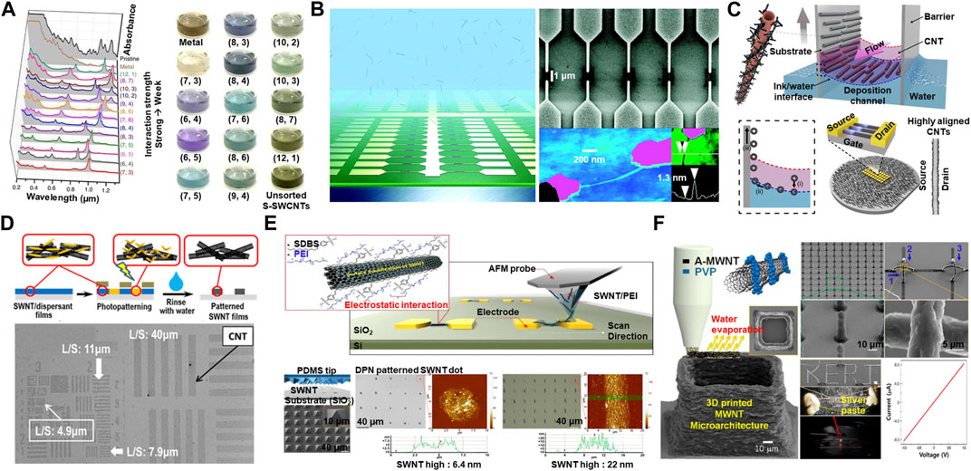
FIGURE 2. Top-down patterning methods using CNTs containing inks. (A) Large-scale SWCNTs separation by gel chromatography method (Liu et al., 2011) (Copyright 2011; Nature). (B) Individual SWCNTs selectively deposited between Au electrodes in a large area by the DEP method (Vijayaraghavan et al., 2007) (Copyright 2007; American Chemical Society). (C) Wafer-scale well-aligned SWCNTs by 2D nematic tangential flow interfacial self-assembly method (Jinkins et al., 2021) (Copyright 2021; Science). (D) Photopatterned SWCNTs thin films utilizing the adsorption/desorption processes of photofunctional dispersants (Matsuzawa et al., 2016) (Copyright 2016; American Chemical Society). (E) SWCNT bundles patterned at high yield via a direct-write DPN process using a SWCNT/SDBS/PEI composite ink (Lee et al., 2016) (Copyright 2016; American Chemical Society). (F) Three-dimensional printing of highly conductive MWCNTs microarchitectures made with fluid inks (Kim et al., 2016a) (Copyright 2016; American Chemical Society).
2.2.1 CNTs patterning/assembly using dielectrophoresis (DEP)
DEP is a CNT patterning method that allows for a precise placement of an individual CNTs with high accuracy (Fishbine, 1996; Yamamoto et al., 1996; Krupke et al., 2003; Baik et al., 2004). Another study showed DEP used to assemble group/ensemble of 50 SWCNTs with high density between graphene electrodes separated by ∼ 1 µm (Engel et al., 2018). A recent study demonstrated that an individual SWCNT-devices can be produced with high density over the large area on a chip using a DEP with only one of its surface electrodes directly connected to an RF source, as compared to a traditional two-electrode geometry. (Figure 2B) (Vijayaraghavan et al., 2007). Overall, DEP patterning techniques are scalable and could be used for advanced device fabrication, but the need for batch processing and specific substrates with pre-patterned electrodes somewhat limit the applications.
2.2.2 Lithographic patterning of CNT films on the substrates
For fabrication and patterning of uniform and aligned CNTs onto the desired substrate and ensures precise and organized arrangement, researchers have experimented with shear, vacuum filtration, directed evaporation, evaporative self-assembly, elastomeric release, dimension-limited self-alignment, DNA-directed assembly, Langmuir-Blodgett, and Langmuir-Schaefer methods etc., for making aligned arrays of CNTs (Xiong et al., 2007; Abdulla and Pullithadathil, 2020; Bodik et al., 2020; Liu et al., 2020). The flow interfacial self-assembly method, recently reported, can create high-density SWCNT ensembles (arrays) with excellent alignment as shown in Figure 2C (Jinkins et al., 2021).
In another method researchers used the SWCNTs dispersed in a solution containing photosensitive dispersant (Matsuzawa et al., 2016). Coating this solution onto a substrate and exposing to UV light through a photomask causes the SWCNTs to aggregate onto the substrate at UV-patterned regions (Figure 2D), while areas not exposed to the UV light were easily dissolved in water and removed. Wang et al. showed a similar method using a photosensitive polyfluorene-based copolymer as an alternative dispersing agent that only reacts and sticks to the substrate when it is exposed to UV light (Wang et al., 2020). Many of these techniques are scalable, and capable to achieve nanoscale features with cutting-edge UV lithography equipment and appropriate dispersing agents.
2.2.3 Patterning and printing of CNTs containing inks
As previously discussed in Section 2.1.3 DPN technology using various cantilevers can pattern individual SWCNTs at nanoscale resolution using catalyst precursor inks (Chen et al., 2011; Farahani et al., 2012). However, as discussed earlier such serial patterning processes could achieve higher throughput when multi-pen tip arrays are employed (Kuljanishvili et al., 2009). Recent studies showed how multi-pen tip arrays (approximately ∼90,000 PDMS pen arrays) were used to pattern SWCNT-bundles containing inks onto the substrate (Figure 2E) (Lee et al., 2016). Authors used ink made of SWCNTs mixed with polyethyleneimine (PEI) in water to create patterns of SWCNTs on SiO2/Si substrates. The line width of the patterned SWCNT-array ranged from 2 μm to 8 nm. Authors demonstrated multiple SWCNT-bundles dot and line patterns, with high throughput.
Advances in printing technologies, also inspire simple and inexpensive techniques for generating CNT patterns (Compton and Lewis, 2014; Lewicki et al., 2017). Authors describe a method for a fast and economical way to print electrical circuits on flexible substrates using MWCNTs-dispersion inks (Kim et al., 2016a). Figure 2F shows a meniscus-guided 3D printing method which was used to make MWCNTs microarchitectures with high spatial resolution, using low viscosity MWCNTs-dispersion inks. The ink was obtained from MWCNTs mixed with polyvinylpyrrolidone (PVP) used as a stabilizer, and the 17 wt% PVP concentration was reported to be optimal for the right viscosity for the ink and ensured uniform patterning. The study demonstrated the fabrication of various 3D MWCNT microstructures, including pillars, bridges, walls, stairs, and alphanumeric shapes. These printing methods, while fast and economical, impose limitations on the resulting products which could suffer from structural and performance deterioration over time.
3 CNTs-based device applications
CNTs have shown great promise in high-performance electronic devices, sometimes surpassing conventional materials. Applications include patterned semiconductor SWCNTs and simple integrated circuit (IC) designs with CNTs (McEuen, 1998; Tans et al., 1998; Franklin et al., 2012; 2022; Franklin, 2013; Wu et al., 2013). CNTFETs are also well-suited RF devices and are compatible with 5G millimeter wave wireless technology (Zhong et al., 2019). Also, recent work has shown CNFETs to deliver higher currents than silicon devices (Yao et al., 1999; Collins et al., 2001; Misewich et al., 2003; Park et al., 2012; Cao et al., 2017; Yang et al., 2017).
High surface area-to-volume ratio and good electrical conductivity of CNTs make them ideal for sensor applications (Wong et al., 1998; Besteman et al., 2003; Modi et al., 2003; Gooding, 2005; Gielen et al., 2016). The immobilization of biomolecules on CNTs enables fast and accurate gas detection and biosensing, and their mechanical robustness extends the stability and lifetime of the sensor. Combining CNTs with microelectromechanical systems (MEMS) and microfluidic devices makes devices/sensors more accurate, and better suited for a point-of-care medical applications, as well as in optical and photonic applications (Rueckes et al., 2000; Fennimore et al., 2003; Stampfer et al., 2006; Rutherglen and Burke, 2007).
In contrast to traditional/conventional silicon-based FETs, the CNTFETs can be used with flexible substrates for wearable electronics (Feng et al., 2010; Lipomi et al., 2011; Noh et al., 2011; Sun et al., 2011; Wang et al., 2012; Son et al., 2015). However, current high resolution patterning methods in most cases are limited to rigid substrates and involve slow and costly processes; photolithography or EBL. Developing innovative high throughput and high-resolution patterning techniques for fabricating CNTs with high density, alignment, chiral selectivity, and structural integrity, is critical for realizing the full potential of CNT-based ICs.
Recent advancements in computing have inspired quantum and neuromorphic computing. These innovative approaches employ quantum mechanics principles and mimic the structure of the biological neural network. Quantum computing uses principles such as superposition and entanglement to perform computations in ways that conventional computers cannot. Researchers use the quantum properties of individual CNTs to create qubits, which are the basic units of quantum information (Gao et al., 2018; Cubaynes et al., 2019; Khivrich and Ilani, 2020; Pistolesi et al., 2021; Baydin et al., 2022). Neuromorphic computing is based on the structure of the human brain, (Kim et al., 2017; Tanaka et al., 2018; Tanim et al., 2022; Xia et al., 2022; Liu et al., 2023). Combining the both methods could lead to more advanced AI systems that use quantum computing to speed up processing and neuromorphic structures to learn and adapt quickly. However, to fully realize the potential of quantum and neuromorphic computing using patterned CNTs technologies, challenges must be overcome. Due to environmental noise and decoherence, it is difficult to ensure stability and control of quantum states in nanotube-based qubits that have defects or vacancies. New computing platforms enabled by CNTs can be a groundbreaking technological achievement which could revolutionize many fields from artificial intelligence and cognitive computing to encryption and optimization.
4 Conclusion and outlook
Continued advances in fabrication and patterning of CNTs at micro- and nanoscale are essential is the key to creating high-performance devices that can transform many industries. Several milestones must be achieved such as large-scale controlled synthesis, consistent production of high quality CNTs delivered by post-synthesis sorting, or via selective controlled synthesis. Continued advances in synthetic methods of growth and patterning or CNTs will be needed. As researchers continue to improve manufacturing techniques, mitigate technological challenges, and exploit the full extent of these approaches, a new era in computing could lead to transformative advances in science and technology.
Author contributions
YK: Conceptualization, Investigation, Methodology, Writing–original draft. IK: Conceptualization, Funding acquisition, Investigation, Methodology, Project administration, Resources, Supervision, Writing–review and editing.
Funding
The authors declare financial support was received for the research, authorship, and/or publication of this article.
Acknowledgments
IK acknowledges support of SLU seed funds, this work was partially supported by Billiken Boost Program sponsored and funded by the Provost’s Office in collaboration with the Faculty Gender Equity Committee, Faculty Fellow for Equity Issues, and the Division of Diversity and Innovative Community Engagement.
Conflict of interest
The authors declare that the research was conducted in the absence of any commercial or financial relationships that could be construed as a potential conflict of interest.
Publisher’s note
All claims expressed in this article are solely those of the authors and do not necessarily represent those of their affiliated organizations, or those of the publisher, the editors and the reviewers. Any product that may be evaluated in this article, or claim that may be made by its manufacturer, is not guaranteed or endorsed by the publisher.
References
Abdulla, S., and Pullithadathil, B. (2020). Unidirectional Langmuir–Blodgett-Mediated alignment of polyaniline-functionalized multiwalled carbon nanotubes for NH3 gas sensor applications. Langmuir 36, 11618–11628. doi:10.1021/acs.langmuir.0c02200
Ahn, J. H., Na, M., Koo, S., Chun, H., Kim, I., Hur, J. W., et al. (2019). Development of a fully automated desktop chemical vapor deposition system for programmable and controlled carbon nanotube growth. Micro Nano Syst. Lett. 7, 11. doi:10.1186/s40486-019-0091-8
Aqel, A., El-Nour, K. M. A., Ammar, R. A. A., and Al-Warthan, A. (2012). Carbon nanotubes, science and technology part (I) structure, synthesis and characterisation. Arabian J. Chem. 5, 1–23. doi:10.1016/j.arabjc.2010.08.022
Arepalli, S. (2004). Laser ablation process for single-walled carbon nanotube production. J. Nanosci. Nanotechnol. 4, 317–325. doi:10.1166/jnn.2004.072
Arnold, M. S., Green, A. A., Hulvat, J. F., Stupp, S. I., and Hersam, M. C. (2006). Sorting carbon nanotubes by electronic structure using density differentiation. Nat. Nanotechnol. 1, 60–65. doi:10.1038/nnano.2006.52
Baik, S., Usrey, M., Rotkina, L., and Strano, M. (2004). Using the selective functionalization of metallic single-walled carbon nanotubes to control dielectrophoretic mobility. J. Phys. Chem. B 108, 15560–15564. doi:10.1021/jp048066u
Baker, R. T. K. (1989). Catalytic growth of carbon filaments. Carbon 27, 315–323. doi:10.1016/0008-6223(89)90062-6
Baker, R. T. K., Harris, P. S., Thomas, R. B., and Waite, R. J. (1973). Formation of filamentous carbon from iron, cobalt and chromium catalyzed decomposition of acetylene. J. Catal. 30, 86–95. doi:10.1016/0021-9517(73)90055-9
Bati, A. S. R., Yu, L., Batmunkh, M., and Shapter, J. G. (2018). Synthesis, purification, properties and characterization of sorted single-walled carbon nanotubes. Nanoscale 10, 22087–22139. doi:10.1039/c8nr07379a
Baydin, A., Tay, F., Fan, J., Manjappa, M., Gao, W., and Kono, J. (2022). Carbon nanotube devices for quantum technology. Materials 15, 1535. doi:10.3390/ma15041535
Bennett, R. D., Hart, A. J., Miller, A. C., Hammond, P. T., Irvine, D. J., and Cohen, R. E. (2006). Creating patterned carbon nanotube catalysts through the microcontact printing of block copolymer micellar thin films. Langmuir 22, 8273–8276. doi:10.1021/la061054a
Besteman, K., Lee, J.-O., Wiertz, F. G. M., Heering, H. A., and Dekker, C. (2003). Enzyme-coated carbon nanotubes as single-molecule biosensors. Nano Lett. 3, 727–730. doi:10.1021/nl034139u
Bodik, M., Maxian, O., Hagara, J., Nadazdy, P., Jergel, M., Majkova, E., et al. (2020). Langmuir–Scheaffer technique as a method for controlled alignment of 1D materials. Langmuir 36, 4540–4547. doi:10.1021/acs.langmuir.0c00045
Cao, Q., Tersoff, J., Farmer, D. B., Zhu, Y., and Han, S.-J. (2017). Carbon nanotube transistors scaled to a 40-nanometer footprint. Science 356, 1369–1372. doi:10.1126/science.aan2476
Cao, Q., Yu, Q., Connell, D. W., and Yu, G. (2013). Titania/carbon nanotube composite (TiO2/CNT) and its application for removal of organic pollutants. Clean Technol. Environ. Policy 15, 871–880. doi:10.1007/s10098-013-0581-y
Carpena-Núñez, J., Davis, B., Islam, A. E., Brown, J., Sargent, G., Murphy, N., et al. (2018). Water-assisted, electron-beam induced activation of carbon nanotube catalyst supports for mask-less, resist-free patterning. Carbon 135, 270–277. doi:10.1016/j.carbon.2018.03.042
Chandra, B., Park, H., Maarouf, A., Martyna, G. J., and Tulevski, G. S. (2011). Carbon nanotube thin film transistors on flexible substrates. Appl. Phys. Lett. 99, 072110. doi:10.1063/1.3622767
Chen, P., Fu, Y., Aminirad, R., Wang, C., Zhang, J., Wang, K., et al. (2011). Fully printed separated carbon nanotube thin film transistor circuits and its application in organic light emitting diode control. Nano Lett. 11, 5301–5308. doi:10.1021/nl202765b
Chinnappan, A., Baskar, C., Kim, H., and Ramakrishna, S. (2016). Carbon nanotube hybrid nanostructures: future generation conducting materials. J. Mat. Chem. A 4, 9347–9361. doi:10.1039/c6ta01717g
Choi, J., Koh, K., and Kim, J. (2013). Scalable and number-controlled synthesis of carbon nanotubes by nanostencil lithography. Nanoscale Res. Lett. 8, 281. doi:10.1186/1556-276x-8-281
Collins, P. G., Arnold, M. S., and Avouris, P. (2001). Engineering carbon nanotubes and nanotube circuits using electrical breakdown. Science 292, 706–709. doi:10.1126/science.1058782
Compton, B. G., and Lewis, J. A. (2014). 3D-Printing of lightweight cellular composites. Adv. Mat. 26, 5930–5935. doi:10.1002/adma.201401804
Cubaynes, T., Delbecq, M. R., Dartiailh, M. C., Assouly, R., Desjardins, M. M., Contamin, L. C., et al. (2019). Highly coherent spin states in carbon nanotubes coupled to cavity photons. npj Quantum Inf. 5, 47. doi:10.1038/s41534-019-0169-4
Dai, H. (2002a). Carbon nanotubes: opportunities and challenges. Surf. Sci. 500, 218–241. doi:10.1016/s0039-6028(01)01558-8
Dai, H. (2002b). Carbon nanotubes: synthesis, integration, and properties. Acc. Chem. Res. 35, 1035–1044. doi:10.1021/ar0101640
De Volder, M. F. L., Tawfick, S. H., Baughman, R. H., and Hart, A. J. (2013). Carbon nanotubes: present and future commercial applications. Science 339, 535–539. doi:10.1126/science.1222453
Ding, L., Zhou, W., Chu, H., Jin, Z., Zhang, Y., and Li, Y. (2006). Direct preparation and patterning of iron oxide nanoparticles via microcontact printing on silicon wafers for the growth of single-walled carbon nanotubes. Chem. Mat. 18, 4109–4114. doi:10.1021/cm061122e
Dong, X., Li, B., Wei, A., Cao, X., Chan-Park, M. B., Zhang, H., et al. (2011). One-step growth of graphene–carbon nanotube hybrid materials by chemical vapor deposition. Carbon 49, 2944–2949. doi:10.1016/j.carbon.2011.03.009
Dresselhaus, M. S., Dresselhaus, G., Saito, R., and Jorio, A. (2005). Raman spectroscopy of carbon nanotubes. Phys. Rep. 409, 47–99. doi:10.1016/j.physrep.2004.10.006
Engel, M., Farmer, D. B., Azpiroz, J. T., Seo, J.-W. T., Kang, J., Avouris, P., et al. (2018). Graphene-enabled and directed nanomaterial placement from solution for large-scale device integration. Nat. Commun. 9, 4095. doi:10.1038/s41467-018-06604-4
Fan, S., Chapline, M. G., Franklin, N. R., Tombler, T. W., Cassell, A. M., and Dai, H. (1999). Self-oriented regular arrays of carbon nanotubes and their field emission properties. Science 283, 512–514. doi:10.1126/science.283.5401.512
Fan, Z., Yan, J., Zhi, L., Zhang, Q., Wei, T., Feng, J., et al. (2010). A three-dimensional carbon nanotube/graphene sandwich and its application as electrode in supercapacitors. Adv. Mater. 22, 3723–3728. doi:10.1002/adma.201001029
Farahani, R. D., Dalir, H., Le Borgne, V., Gautier, L. A., El Khakani, M. A., Lévesque, M., et al. (2012). Direct-write fabrication of freestanding nanocomposite strain sensors. Nanotechnology 23, 085502. doi:10.1088/0957-4484/23/8/085502
Feng, C., Liu, K., Wu, J., Liu, L., Cheng, J., Zhang, Y., et al. (2010). Flexible, stretchable, transparent conducting films made from superaligned carbon nanotubes. Adv. Funct. Mat. 20, 885–891. doi:10.1002/adfm.200901960
Fennimore, A. M., Yuzvinsky, T. D., Han, W.-Q., Fuhrer, M. S., Cumings, J., and Zettl, A. (2003). Rotational actuators based on carbon nanotubes. Nature 424, 408–410. doi:10.1038/nature01823
Fishbine, B. H. (1996). Carbon nanotube alignment and manipulation using electrostatic fields. Fullerene Sci. Technol. 4, 87–100. doi:10.1080/10641229608001539
Franklin, A. D., Hersam, M. C., and Wong, H.-S. P. (2022). Carbon nanotube transistors: making electronics from molecules. Science 378, 726–732. doi:10.1126/science.abp8278
Franklin, A. D., Luisier, M., Han, S.-J., Tulevski, G., Breslin, C. M., Gignac, L., et al. (2012). Sub-10 nm carbon nanotube transistor. Nano Lett. 12, 758–762. doi:10.1021/nl203701g
Franklin, A. D. (2013). The road to carbon nanotube transistors. Nature 498, 443–444. doi:10.1038/498443a
Freer, E. M., Grachev, O., Duan, X., Martin, S., and Stumbo, D. P. (2010). High-yield self-limiting single-nanowire assembly with dielectrophoresis. Nat. Nanotechnol. 5, 525–530. doi:10.1038/nnano.2010.106
Gao, W., Li, X., Bamba, M., and Kono, J. (2018). Continuous transition between weak and ultrastrong coupling through exceptional points in carbon nanotube microcavity exciton–polaritons. Nat. Photonics 12, 362–367. doi:10.1038/s41566-018-0157-9
Gavillet, J., Loiseau, A., Journet, C., Willaime, F., Ducastelle, F., and Charlier, J.-C. (2001). Root-growth mechanism for single-wall carbon nanotubes. Phys. Rev. Lett. 87, 275504. doi:10.1103/physrevlett.87.275504
Gielen, G., Van Rethy, J., Marin, J., Shulaker, M. M., Hills, G., Wong, H.-S. P., et al. (2016). Time-based sensor interface circuits in CMOS and carbon nanotube technologies. IEEE Trans. Circuits Syst. I Regul. Pap. 63, 577–586. doi:10.1109/tcsi.2016.2525098
Gooding, J. J. (2005). Nanostructuring electrodes with carbon nanotubes: A review on electrochemistry and applications for sensing. Electrochimica Acta 50, 3049–3060. doi:10.1016/j.electacta.2004.08.052
Guo, T., Nikolaev, P., Thess, A., Colbert, D. T., and Smalley, R. E. (1995). Catalytic growth of single-walled manotubes by laser vaporization. Chem. Phys. Lett. 243, 49–54. doi:10.1016/0009-2614(95)00825-o
Häffner, M., Haug, A., Weitz, R. T., Fleischer, M., Burghard, M., Peisert, H., et al. (2008). E-beam lithography of catalyst patterns for carbon nanotube growth on insulating substrates. Microelectron. Eng. 85, 768–773. doi:10.1016/j.mee.2008.01.046
Hameed, A., Mukhtar, A., Shafiq, U., Qizilbash, M., Khan, M. S., Rashid, T., et al. (2019). Experimental investigation on synthesis, characterization, stability, thermo-physical properties and rheological behavior of MWCNTs-kapok seed oil based nanofluid. J. Mol. Liq. 277, 812–824. doi:10.1016/j.molliq.2019.01.012
Hodge, S. A., Bayazit, M. K., Coleman, K. S., and Shaffer, M. S. P. (2012). Unweaving the rainbow: A review of the relationship between single-walled carbon nanotube molecular structures and their chemical reactivity. Chem. Soc. Rev. 41, 4409–4429. doi:10.1039/c2cs15334c
Hong, S. W., Banks, T., and Rogers, J. A. (2010). Improved density in aligned arrays of single-walled carbon nanotubes by sequential chemical vapor deposition on quartz. Adv. Mat. 22, 1826–1830. doi:10.1002/adma.200903238
Hu, H., Kim, H., and Somnath, S. (2017). Tip-based nanofabrication for scalable manufacturing. Micromachines 8, 90. doi:10.3390/mi8030090
Hu, L., Hecht, D. S., and Gruner, G. (2010). Carbon nanotube thin films: fabrication, properties, and applications. Chem. Rev. 110, 5790–5844. doi:10.1021/cr9002962
Huang, S., Mau, A. W. H., Turney, T. W., White, P. A., and Dai, L. (2000). Patterned growth of well-aligned carbon nanotubes: A soft-lithographic approach. J. Phys. Chem. B 104, 2193–2196. doi:10.1021/jp994152w
Ibrahim, K. S. (2013). Carbon nanotubes-properties and applications: A review. Carbon Lett. 14, 131–144. doi:10.5714/cl.2013.14.3.131
Iijima, S. (1991). Helical microtubules of graphitic carbon. Nature 354, 56–58. doi:10.1038/354056a0
Iijima, S., and Ichihashi, T. (1993). Single-shell carbon nanotubes of 1-nm diameter. Nature 363, 603–605. doi:10.1038/363603a0
Imaizumi, Y., Arakawa, Y., Arai, F., and Fukuda, T. (2005). “Local growth of carbon nanotubes on the cantilever by chemical vapor deposition with fib assist etching,” in 5th IEEE Conf. Nanotechnol., 2005, Nagoya, Japan, 15-15 July 2005 (IEEE), 1–4. doi:10.1109/nano.2005.1500850
Ishida, M., Hongo, H., Nihey, F., and Ochiai, Y. (2004). Diameter-controlled carbon nanotubes grown from lithographically defined nanoparticles. Jpn. J. Appl. Phys. 43, L1356–L1358. doi:10.1143/jjap.43.l1356
Javey, A., and Dai, H. (2005). Regular arrays of 2 nm metal nanoparticles for deterministic synthesis of nanomaterials. J. Am. Chem. Soc. 127, 11942–11943. doi:10.1021/ja0536668
Javey, A., Guo, J., Farmer, D. B., Wang, Q., Yenilmez, E., Gordon, R. G., et al. (2004). Self-aligned ballistic molecular transistors and electrically parallel nanotube arrays. Nano Lett. 4, 1319–1322. doi:10.1021/nl049222b
Jinkins, K. R., Foradori, S. M., Saraswat, V., Jacobberger, R. M., Dwyer, J. H., Gopalan, P., et al. (2021). Aligned 2D carbon nanotube liquid crystals for wafer-scale electronics. Sci. Adv. 7, eabh0640. doi:10.1126/sciadv.abh0640
José-Yacamán, M., Terrones, H., Rendón, L., and Domínguez, J. M. (1995). Carbon structures grown from decomposition of a phenylacetylene and thiophene mixture on Ni nanoparticles. Carbon 33, 669–678. doi:10.1016/0008-6223(94)00154-r
Jung, H. K., and Lee, H. W. (2014). Effect of catalytic layer thickness on diameter of vertically aligned individual carbon nanotubes. J. Nanomater. 2014, 1–6. doi:10.1155/2014/270989
Kataura, H., Kumazawa, Y., Maniwa, Y., Umezu, I., Suzuki, S., Ohtsuka, Y., et al. (1999). Optical properties of single-wall carbon nanotubes. Synth. Met. 103, 2555–2558. doi:10.1016/s0379-6779(98)00278-1
Kempa, K., Kimball, B., Rybczynski, J., Huang, Z. P., Wu, P. F., Steeves, D., et al. (2003). Photonic crystals based on periodic arrays of aligned carbon nanotubes. Nano Lett. 3, 13–18. doi:10.1021/nl0258271
Khivrich, I., and Ilani, S. (2020). Atomic-like charge qubit in a carbon nanotube enabling electric and magnetic field nano-sensing. Nat. Commun. 11, 2299. doi:10.1038/s41467-020-16001-5
Kim, J. H., Lee, S., Wajahat, M., Jeong, H., Chang, W. S., Jeong, H. J., et al. (2016a). Three-dimensional printing of highly conductive carbon nanotube microarchitectures with fluid ink. ACS Nano 10, 8879–8887. doi:10.1021/acsnano.6b04771
Kim, S., Choi, B., Lim, M., Yoon, J., Lee, J., Kim, H.-D., et al. (2017). Pattern recognition using carbon nanotube synaptic transistors with an adjustable weight update protocol. ACS Nano 11, 2814–2822. doi:10.1021/acsnano.6b07894
Kim, S., Sojoudi, H., Zhao, H., Mariappan, D., McKinley, G. H., Gleason, K. K., et al. (2016b). Ultrathin high-resolution flexographic printing using nanoporous stamps. Sci. Adv. 2, e1601660. doi:10.1126/sciadv.1601660
Kind, H., Bonard, J. M., Emmenegger, C., Nilsson, L. O., Hernadi, K., Maillard-Schaller, E., et al. (1999). Patterned films of nanotubes using microcontact printing of catalysts. Adv. Mat. 11, 1285–1289. doi:10.1002/(sici)1521-4095(199910)11:15<1285:aid-adma1285>3.0.co;2-j
King, S. G., McCafferty, L., Tas, M. O., Snashall, K., Chen, J. S., Shkunov, M., et al. (2020). Low-cost catalyst ink for simple patterning and growth of high-quality single- and double-walled carbon nanotubes. ACS Appl. Mat. Interfaces 12, 11898–11906. doi:10.1021/acsami.9b19957
Kociak, M., Kasumov, A.Yu., Guéron, S., Reulet, B., Khodos, I. I., Gorbatov, Yu. B., et al. (2001). Superconductivity in ropes of single-walled carbon nanotubes. Phys. Rev. Lett. 86, 2416–2419. doi:10.1103/physrevlett.86.2416
Kroto, H. W., Heath, J. R., O’Brien, S. C., Curl, R. F., and Smalley, R. E. (1985). C60: buckminsterfullerene. Nature 318, 162–163. doi:10.1038/318162a0
Krupke, R., Hennrich, F., Weber, H. B., Kappes, M. M., and v Löhneysen, H. (2003). Simultaneous deposition of metallic bundles of single-walled carbon nanotubes using Ac-dielectrophoresis. Nano Lett. 3, 1019–1023. doi:10.1021/nl0342343
Kuljanishvili, I., Dikin, D. A., Rozhok, S., Mayle, S., and Chandrasekhar, V. (2009). Controllable patterning and CVD growth of isolated carbon nanotubes with direct parallel writing of catalyst using dip-pen nanolithography. Small 5, 2523–2527. doi:10.1002/smll.200900841
Kumar, M., and Ando, Y. (2010). Chemical vapor deposition of carbon nanotubes: A review on growth mechanism and mass production. J. Nanosci. Nanotechnol. 10, 3739–3758. doi:10.1166/jnn.2010.2939
Kunitoshi Yamamoto, K. Y., Seiji Akita, S. A., and Yoshikazu Nakayama, Y. N. (1996). Orientation of carbon nanotubes using electrophoresis. Jpn. J. Appl. Phys. 35, L917. doi:10.1143/jjap.35.l917
Lee, D. H., Shin, D. O., Lee, W. J., and Kim, S. O. (2008). Hierarchically organized carbon nanotube arrays from self-assembled block copolymer nanotemplates. Adv. Mat. 20, 2480–2485. doi:10.1002/adma.200702712
Lee, J.-H., Najeeb, C. K., Nam, G.-H., Shin, Y., Lim, J.-H., and Kim, J.-H. (2016). Large-scale direct patterning of aligned single-walled carbon nanotube arrays using dip-pen nanolithography. Chem. Mat. 28, 6471–6476. doi:10.1021/acs.chemmater.6b01075
Lewicki, J. P., Rodriguez, J. N., Zhu, C., Worsley, M. A., Wu, A. S., Kanarska, Y., et al. (2017). 3D-Printing of meso-structurally ordered carbon fiber/polymer composites with unprecedented orthotropic physical properties. Sci. Rep. 7, 43401. doi:10.1038/srep43401
Li, B., Goh, C. F., Zhou, X., Lu, G., Tantang, H., Chen, Y., et al. (2008). Patterning colloidal metal nanoparticles for controlled growth of carbon nanotubes. Adv. Mater. 20, 4873–4878. doi:10.1002/adma.200802306
Li, W. Z., Xie, S. S., Qian, L. X., Chang, B. H., Zou, B. S., Zhou, W. Y., et al. (1996). Large-scale synthesis of aligned carbon nanotubes. Science 274, 1701–1703. doi:10.1126/science.274.5293.1701
Li, Y.-L., Kinloch, I. A., Shaffer, M. S. P., Geng, J., Johnson, B., and Windle, A. H. (2004). Synthesis of single-walled carbon nanotubes by a fluidized-bed method. Chem. Phys. Lett. 384, 98–102. doi:10.1016/j.cplett.2003.11.070
Liang, J., Chen, R., Ramos, R., Lee, J., Okuno, H., Kalita, D., et al. (2019). Investigation of Pt-Salt-Doped-Standalone- multiwall carbon nanotubes for on-chip interconnect applications. IEEE Trans. Electron Devices 66, 2346–2352. doi:10.1109/ted.2019.2901658
Liang, R.-P., Wang, Z.-X., Zhang, L., and Qiu, J.-D. (2012). A label-free amperometric immunosensor for alpha-fetoprotein determination based on highly ordered porous multi-walled carbon nanotubes/silica nanoparticles array platform. Sensors Actuators B Chem. 166-167, 569–575. doi:10.1016/j.snb.2012.03.011
Liang, W., Bockrath, M., Bozovic, D., Hafner, J. H., Tinkham, M., and Park, H. (2001). Fabry - perot interference in a nanotube electron waveguide. Nature 411, 665–669. doi:10.1038/35079517
Lipomi, D. J., Vosgueritchian, M., Tee, B. C.-K., Hellstrom, S. L., Lee, J. A., Fox, C. H., et al. (2011). Skin-like pressure and strain sensors based on transparent elastic films of carbon nanotubes. Nat. Nanotechnol. 6, 788–792. doi:10.1038/nnano.2011.184
Liu, H., Nishide, D., Tanaka, T., and Kataura, H. (2011). Large-scale single-chirality separation of single-wall carbon nanotubes by simple gel chromatography. Nat. Commun. 2, 309. doi:10.1038/ncomms1313
Liu, L., Han, J., Xu, L., Zhou, J., Zhao, C., Ding, S., et al. (2020). Aligned, high-density semiconducting carbon nanotube arrays for high-performance electronics. Science 368, 850–856. doi:10.1126/science.aba5980
Liu, R., Kim, J. G., Dhakal, P., Li, W., Ma, J., Hou, A., et al. (2023). Neuromorphic properties of flexible carbon nanotube/polydimethylsiloxane nanocomposites. Adv. Compos. Hybrid. Mat. 6, 14. doi:10.1007/s42114-022-00599-9
Matsuzawa, Y., Takada, Y., Jintoku, H., Kihara, H., and Yoshida, M. (2016). Photopatterned single-walled carbon nanotube films utilizing the adsorption/desorption processes of photofunctional dispersants. ACS Appl. Mat. Interfaces 8, 28400–28405. doi:10.1021/acsami.6b06169
Meyyappan, M., Delzeit, L., Cassell, A., and Hash, D. (2003). Carbon nanotube growth by PECVD: A review. Plasma Sources Sci. Technol. 12, 205–216. doi:10.1088/0963-0252/12/2/312
Misewich, J. A., Martel, R., Avouris, Ph., Tsang, J. C., Heinze, S., and Tersoff, J. (2003). Electrically induced optical emission from a carbon nanotube FET. Science 300, 783–786. doi:10.1126/science.1081294
Modi, A., Koratkar, N., Lass, E., Wei, B., and Ajayan, P. M. (2003). Miniaturized gas ionization sensors using carbon nanotubes. Nature 424, 171–174. doi:10.1038/nature01777
Moore, K. E., Tune, D. D., and Flavel, B. S. (2015). Double-Walled carbon nanotube processing. Adv. Mat. 27, 3105–3137. doi:10.1002/adma.201405686
Nish, A., Hwang, J.-Y., Doig, J., and Nicholas, R. J. (2007). Highly selective dispersion of single-walled carbon nanotubes using aromatic polymers. Nat. Nanotechnol. 2, 640–646. doi:10.1038/nnano.2007.290
Noh, J., Jung, M., Jung, K., Lee, G., Kim, J., Lim, S., et al. (2011). Fully gravure-printed D flip-flop on plastic foils using single-walled carbon-nanotube-based TFTs. IEEE Electron Device Lett. 32, 638–640. doi:10.1109/led.2011.2118732
Novoselov, K. (2009). Beyond the wonder material. Phys. World 22, 27–30. doi:10.1088/2058-7058/22/08/33
Odom, T. W., Huang, J.-L., Kim, P., and Lieber, C. M. (2000). Structure and electronic properties of carbon nanotubes. J. Phys. Chem. B 104, 2794–2809. doi:10.1021/jp993592k
Ono, Y., Kishimoto, S., Ohno, Y., and Mizutani, T. (2010). Thin film transistors using PECVD-grown carbon nanotubes. Nanotechnology 21, 205202. doi:10.1088/0957-4484/21/20/205202
Pander, A., Hatta, A., and Furuta, H. (2017). FIB secondary etching method for fabrication of fine CNT forest metamaterials. Nano-Micro Lett. 9, 44. doi:10.1007/s40820-017-0145-5
Papadopoulos, C., and Omrane, B. (2008). Nanometer-scale catalyst patterning for controlled growth of individual single-walled carbon nanotubes. Adv. Mat. 20, 1344–1347. doi:10.1002/adma.200701881
Park, H., Afzali, A., Han, S.-J., Tulevski, G. S., Franklin, A. D., Tersoff, J., et al. (2012). High-density integration of carbon nanotubes via chemical self-assembly. Nat. Nanotechnol. 7, 787–791. doi:10.1038/nnano.2012.189
Patil, N., Lin, A., Myers, E. R., Ryu, K., Badmaev, A., Zhou, C., et al. (2009a). Wafer-scale growth and transfer of aligned single-walled carbon nanotubes. IEEE Trans. Nanotechnol. 8, 498–504. doi:10.1109/tnano.2009.2016562
Patil, N., Lin, A., Zhang, J., Wei, H., Anderson, K., Wong, H.-S. P., et al. (2009b). “Vmr: VLSI-compatible metallic carbon nanotube removal for imperfection-immune cascaded multi-stage digital logic circuits using carbon nanotube FETs,” in 2009 IEEE int. Electron devices meet. (IEDM), 1–4. doi:10.1109/iedm.2009.5424295
Piner, R. D., Zhu, J., Xu, F., Hong, S., and Mirkin, C. A. (1999). “Dip-Pen” nanolithography. Science 283, 661–663. doi:10.1126/science.283.5402.661
Pistolesi, F., Cleland, A. N., and Bachtold, A. (2021). Proposal for a nanomechanical qubit. Phys. Rev. X 11, 031027. doi:10.1103/physrevx.11.031027
Polsen, E. S., Stevens, A. G., and Hart, A. J. (2013). Laser printing of nanoparticle toner enables digital control of micropatterned carbon nanotube growth. ACS Appl. Mat. Interfaces 5, 3656–3662. doi:10.1021/am400148t
Rueckes, T., Kim, K., Joselevich, E., Tseng, G. Y., Cheung, C.-L., and Lieber, C. M. (2000). Carbon nanotube-based nonvolatile random access memory for molecular computing. Science 289, 94–97. doi:10.1126/science.289.5476.94
Rutherglen, C., and Burke, P. (2007). Carbon nanotube radio. Nano Lett. 7, 3296–3299. doi:10.1021/nl0714839
Saito, R., and Dresselhaus, M. S. (1998). Physical properties of carbon nanotubes. London: Imperial College Press. doi:10.1142/p080
Schaper, N., Alameri, D., Kim, Y., Thomas, B., McCormack, K., Chan, M., et al. (2021). Controlled fabrication of quality ZnO NWs/CNTs and ZnO NWs/gr heterostructures via direct two-step CVD method. Nanomaterials 11, 1836. doi:10.3390/nano11071836
Son, D., Koo, J. H., Song, J.-K., Kim, J., Lee, M., Shim, H. J., et al. (2015). Stretchable carbon nanotube charge-trap floating-gate memory and logic devices for wearable electronics. ACS Nano 9, 5585–5593. doi:10.1021/acsnano.5b01848
Stampfer, C., Helbling, T., Obergfell, D., Schöberle, B., Tripp, M. K., Jungen, A., et al. (2006). Fabrication of single-walled carbon-nanotube-based pressure sensors. Nano Lett. 6, 233–237. doi:10.1021/nl052171d
Sun, D., Timmermans, M. Y., Tian, Y., Nasibulin, A. G., Kauppinen, E. I., Kishimoto, S., et al. (2011). Flexible high-performance carbon nanotube integrated circuits. Nat. Nanotechnol. 6, 156–161. doi:10.1038/nnano.2011.1
Tanaka, H., Akai-Kasaya, M., TermehYousefi, A., Hong, L., Fu, L., Tamukoh, H., et al. (2018). A molecular neuromorphic network device consisting of single-walled carbon nanotubes complexed with polyoxometalate. Nat. Commun. 9, 2693. doi:10.1038/s41467-018-04886-2
Tanim, M. M. H., Vicenciodelmoral, A. Y., Templin, Z., Zhao, X., and Zhao, F. (2022). “Honey-CNT based resistive switching device for neuromorphic computing applications,” in 2022 IEEEACM int. Conf. Big data comput., appl. Technol. (BDCAT), 182–183. doi:10.1109/bdcat56447.2022.00034
Tans, S. J., Verschueren, A. R. M., and Dekker, C. (1998). Room-temperature transistor based on a single carbon nanotube. Nature 393, 49–52. doi:10.1038/29954
Tawfick, S., Deng, X., Hart, A. J., and Lahann, J. (2010). Nanocomposite microstructures with tunable mechanical and chemical properties. Phys. Chem. Chem. Phys. 12, 4446–4451. doi:10.1039/c000304m
Tîlmaciu, C.-M., and Morris, M. C. (2015). Carbon nanotube biosensors. Front. Chem. 3, 59. doi:10.3389/fchem.2015.00059
Tu, X., Manohar, S., Jagota, A., and Zheng, M. (2009). DNA sequence motifs for structure-specific recognition and separation of carbon nanotubes. Nature 460, 250–253. doi:10.1038/nature08116
Turaeva, N., Kim, Y., and Kuljanishvili, I. (2023). An extended model for chirality selection in single-walled carbon nanotubes. Nanoscale Adv. 5, 3684–3690. doi:10.1039/d3na00192j
Turaeva, N., and Kuljanishvili, I. (2021). Effects of electronic structure of catalytic nanoparticles on carbon nanotube growth. Carbon Trends 5, 100092. doi:10.1016/j.cartre.2021.100092
Vijayaraghavan, A., Blatt, S., Weissenberger, D., Oron-Carl, M., Hennrich, F., Gerthsen, D., et al. (2007). Ultra-large-scale directed assembly of single-walled carbon nanotube devices. Nano Lett. 7, 1556–1560. doi:10.1021/nl0703727
Volder, M. D., Reynaerts, D., Hoof, C. V., Tawfick, S., and Hart, A. J. (2010). “A temperature sensor from a self-assembled carbon nanotube microbridge,” in 2010 IEEE sens, 2369–2372. doi:10.1109/icsens.2010.5690868
Wang, C., Chien, J.-C., Takei, K., Takahashi, T., Nah, J., Niknejad, A. M., et al. (2012). Extremely bendable, high-performance integrated circuits using semiconducting carbon nanotube networks for digital, analog, and radio-frequency applications. Nano Lett. 12, 1527–1533. doi:10.1021/nl2043375
Wang, K., Dong, H., Zhou, D., Ito, Y., Hu, L., Zhang, Z., et al. (2020). Facile fabrication of semiconducting single-walled carbon nanotubes patterns on flexible substrate based on a photoimmobilization technique. ACS Appl. Mat. Interfaces 12, 8722–8729. doi:10.1021/acsami.9b21142
Wang, Y., Wei, F., Luo, G., Yu, H., and Gu, G. (2002). The large-scale production of carbon nanotubes in a nano-agglomerate fluidized-bed reactor. Chem. Phys. Lett. 364, 568–572. doi:10.1016/s0009-2614(02)01384-2
White, C. T., and Todorov, T. N. (1998). Carbon nanotubes as long ballistic conductors. Nature 393, 240–242. doi:10.1038/30420
Whitsitt, E. A., and Barron, A. R. (2003). Silica coated single walled carbon nanotubes. Nano Lett. 3, 775–778. doi:10.1021/nl034186m
Wong, S. S., Joselevich, E., Woolley, A. T., Cheung, C. L., and Lieber, C. M. (1998). Covalently functionalized nanotubes as nanometre-sized probes in chemistry and biology. Nature 394, 52–55. doi:10.1038/27873
Wu, Y., Lin, X., and Zhang, M. (2013). Carbon nanotubes for thin film transistor: fabrication, properties, and applications. J. Nanomater. 2013, 1–16. doi:10.1155/2013/627215
Wu, Z., Chen, Z., Du, X., Logan, J. M., Sippel, J., Nikolou, M., et al. (2004). Transparent, conductive carbon nanotube films. Science 305, 1273–1276. doi:10.1126/science.1101243
Wu, Z., Gao, S., Chen, L., Jiang, D., Shao, Q., Zhang, B., et al. (2017). Electrically insulated epoxy nanocomposites reinforced with synergistic core–shell SiO2@MWCNTs and montmorillonite bifillers. Macromol. Chem. Phys. 218, 1700357. doi:10.1002/macp.201700357
Xia, F., Xia, T., Xiang, L., Ding, S., Li, S., Yin, Y., et al. (2022). Carbon nanotube-based flexible ferroelectric synaptic transistors for neuromorphic computing. ACS Appl. Mat. Interfaces 14, 30124–30132. doi:10.1021/acsami.2c07825
Xiong, X., Jaberansari, L., Hahm, M. G., Busnaina, A., and Jung, Y. J. (2007). Building highly organized single-walled-carbon-nanotube networks using template-guided fluidic assembly. Small 3, 2006–2010. doi:10.1002/smll.200700292
Yang, Y., Ding, L., Han, J., Zhang, Z., and Peng, L.-M. (2017). High-performance complementary transistors and medium-scale integrated circuits based on carbon nanotube thin films. ACS Nano 11, 4124–4132. doi:10.1021/acsnano.7b00861
Yao, Z., Kane, C. L., and Dekker, C. (2000). High-field electrical transport in single-wall carbon nanotubes. Phys. Rev. Lett. 84, 2941–2944. doi:10.1103/physrevlett.84.2941
Zeng, X., Yang, D., Liu, H., Zhou, N., Wang, Y., Zhou, W., et al. (2018). Detecting and tuning the interactions between surfactants and carbon nanotubes for their high-efficiency structure separation. Adv. Mat. Interfaces 5, 1700727. doi:10.1002/admi.201700727
Zhao, X., Ohkohchi, M., Wang, M., Iijima, S., Ichihashi, T., and Ando, Y. (1997). Preparation of high-grade carbon nanotubes by hydrogen arc discharge. Carbon 35, 775–781. doi:10.1016/s0008-6223(97)00033-x
Zheng, M., Jagota, A., Semke, E. D., Diner, B. A., Mclean, R. S., Lustig, S. R., et al. (2003). DNA-assisted dispersion and separation of carbon nanotubes. Nat. Mater. 2, 338–342. doi:10.1038/nmat877
Zheng, M. (2017). Sorting carbon nanotubes. Top. Curr. Chem. Collect., 129–164. doi:10.1007/978-3-030-12700-8_5
Zhong, D., Shi, H., Ding, L., Zhao, C., Liu, J., Zhou, J., et al. (2019). Carbon nanotube film-based radio frequency transistors with maximum oscillation frequency above 100 GHz. ACS Appl. Mat. Interfaces 11, 42496–42503. doi:10.1021/acsami.9b15334
Keywords: carbon nanotubes, top-down, bottom-up, micro-and nanoscale patterning, carbon nanotube devices, large area CNTs fabrication and printing
Citation: Kim Y and Kuljanishvili I (2023) Recent advances in carbon nanotube patterning technologies for device applications. Front. Carbon 2:1288912. doi: 10.3389/frcrb.2023.1288912
Received: 05 September 2023; Accepted: 22 September 2023;
Published: 03 October 2023.
Edited by:
Anthony B. Dichiara, University of Washington, United StatesReviewed by:
Takahide Oya, Yokohama National University, JapanCopyright © 2023 Kim and Kuljanishvili. This is an open-access article distributed under the terms of the Creative Commons Attribution License (CC BY). The use, distribution or reproduction in other forums is permitted, provided the original author(s) and the copyright owner(s) are credited and that the original publication in this journal is cited, in accordance with accepted academic practice. No use, distribution or reproduction is permitted which does not comply with these terms.
*Correspondence: Irma Kuljanishvili, aXJtYS5rdWxqYW5pc2h2aWxpQHNsdS5lZHU=