Abstract
This paper presents a low-profile, tightly coupled dipole array (TCDA) antenna to achieve broad-angle scanning with excellent impedance matching over a wide bandwidth. The antenna element is innovatively designed using two planar shorted patches, forming a compact structure. A pair of parasitic strips is incorporated between adjacent antenna elements to ensure surface current uniformity across a wide frequency range. A high-index semi-arc metasurface (MS) is engineered as a wide-angle impedance matching (WAIM) layer to enhance the scanning performance in both E− and H-planes without compromising the low-profile form factor. Full-wave simulations demonstrate that the proposed antenna array supports a wide scanning range of up to in both E− and H-planes over an ultra-wide bandwidth of GHz at . A array prototype was fabricated and experimentally tested to validate the design concept. The measurement results exhibit good agreement with simulations, confirming the efficacy and practicability of the proposed TCDA design. The proposed array achieves wideband impedance matching and wide-angle scanning capability within a compact, planar structure, making it highly suitable for mobile satellite communications and emerging 6G systems requiring agile beam steering.
1 Introduction
Over the last few years, satellite communication (SATCOM) has been explored for commercial services, such as television broadcasting and broadband internet services. Many of these applications function in the Ku-band because of its global accessibility and the substantial data rate capacity of satellite services. Furthermore, future 6G communication is anticipated to include Non-terrestrial networks (NTN) in commercial mobile services (Ansari et al., 2021; Xylouris et al., 2024), particularly for automobiles, trains, and aircraft. However, in contrast to traditional SATCOM, which necessitates a large dish reflector antenna, the antenna system utilised in mobile and vehicular platforms for SATCOM must possess a low-profile design and the capability for rapid beam switching. Phased array antennas, distinguished by their flexible beamforming capabilities, high gain, and low profile, have garnered considerable interest in the last few decades for several applications, including radar (Kim et al., 2024; Latha et al., 2021) and 5G communication (Yong and Alayón Glazunov., 2023; Gu et al., 2021). The phased array antenna is also a viable candidate for establishing a communication connection between mobile vehicles and satellite communication, owing to its rapid beam scanning capabilities while maintaining a low profile.
Conventional phased array antennas based on patch antennas are often limited by their bandwidth or scanning capabilities (Li et al., 2023). To realise the phased array antenna with ultra-wideband and wide scanning capabilities, the Vivaldi antenna is a potential candidate (Logan et al., 2018a; Logan et al., 2018b. However, these Vivaldi antennas usually come with a high volumetric profile and nonplanar features, which pose challenges in integrating or installing them into the vehicle. On the other hand, the tightly coupled dipole array (TCDA) has gained significant interest owing to its characteristics of ultrawideband, compact, planar, and wide scanning features (Li et al., 2017; Doane et al., 2013). The design of the TCDA is initially inspired by Wheeler’s theoretical current sheet model, proposed in 1949 (Wheeler, 1965). However, it did not gain significant attention in the earlier years. In the early 2000s, Munk extended Wheeler’s current sheet into the current sheet array (CSA), which turns this theoretical concept into a practical array configuration (Munk, 2003; Munk, 2006). In 2003, the first TCDA phased array antenna with ultrawideband and wide scanning was proposed by Munk et al. (2003). Since then, most TCDA antennas have emerged significantly to achieve ultra-wideband and wide-scanning performance (Lee and Nam, 2017; Zhou et al., 2018; Lee Hakjune and Yoon, 2019; Liang et al., 2020; Zhou et al., 2022; Wen et al., 2024). However, most existing TCDA antennas in publications share a common drawback: a high volumetric profile resulting from their structural configuration. In addition, TCDAs require the balun feeding networks to excite the antenna and ensure proper signal transmission (Lindberg et al., 2007; Shim et al., 2019). However, this approach further contributes to the high volumetric profile due to its nonplanar structure (Doane et al., 2012). As a result, traditional TCDAs consistently struggle to maintain a low volumetric profile while achieving optimal performance.
TCDA antennas often incorporate a well-designed radiating structure and an additional matching layer to achieve ultrawideband and wide-angle performance. This layer, known as the wide-angle impedance matching (WAIM) layer, is placed on top of the phased array to enhance impedance matching and minimise reflection across a wide range of incident angles. The WAIM layer can be realised utilising a simple dielectric substrate on top of the TCDA to enhance impedance matching and scanning capability (the dielectric substrate-based WAIM is also sometimes known as dielectric superstrate) (Gou et al., 2024; Moulder et al., 2013; Papantonis and Volakis, 2015; Moghaddam et al., 2020; Logan et al., 2017). In (Moulder et al., 2013), a dielectric superstrate is employed to realise an extremely wideband across at when scanning up to . Similarly, in (Papantonis and Volakis, 2015), a dielectric superstrate with a thickness of approximately (where is the wavelength of the highest operating frequency) is used to enhance the impedance bandwidth. In Moghaddam et al. (2020), a planar TCDA with a wide scanning range up to is proposed by using a dielectric superstrate. However, a higher profile and an increasing weight limit their applications. To reduce the overall profile of the WAIM, it is proposed to realise the WAIM using either the frequency selective surface (FSS) (Jiang et al., 2020) or metasurface (Sun et al., 2021; Bah et al., 2019). In (Sun et al., 2021), a capacitive metasurface layer is loaded to suppress the in-band coupled-loop modes. A square patch-based metasurface (MS) layer is introduced in Wang et al. (2023) to mitigate the surface waves when scanning in H-plane. In Zhang et al. (2022), an MS layer composed of full-split rings is used to achieve a wide scanning range. Despite these advancements, the mentioned designs commonly operate at low frequencies.
Based on the above discussion, existing TCDA antennas offer unique advantages, including wide-angle scanning capability and ultrawideband performance, making them highly suitable for various advanced communication and data transmission applications. However, despite these benefits, TCDA antennas still face several critical limitations. One major drawback is their inherently high volumetric profile, which arises from their structural configuration, an additional component of balun feeding networks, and the presence of a WAIM layer (superstrate, FSS, and MS). In addition, the complex structure of the TCDA often makes fabrication and implementation more challenging and costly. Moreover, most current designs only apply to frequency bands below the Ku band, limiting their use in higher-frequency communication systems.
This paper uses a low-profile TCDA phased array antenna to support a wide-angle scanning capability of while operating in the 12–30 GHz frequency range. The radiating element consists of a pair of dipole arms with six shorting posts connected to the ground. A -shaped feeding probe is utilised beneath the radiator to maintain a planar structure. In addition, a semi-arc MS layer with a high refractive index is introduced to enhance impedance matching during wide-angle scanning. Moreover, the main advantage of the proposed TCDA phased array is that it is realised using a cost-effective dielectric substrate (Rogers 4350B), and it features a simple and fully planar design, making it attractive for mass production for commercialised industry applications.
The presented low-profile, wideband, wide-scanning phased array antenna addresses critical challenges in next-generation wireless and satellite communication systems, especially for mobile and vehicular platforms. By leveraging a tightly coupled dipole array (TCDA) enhanced with capacitive strips for common-mode suppression and a semi-arc metasurface for wide-angle impedance matching, the design achieves ultra-wideband operation (12–30 GHz), wide-angle scanning capability , and a compact, fully planar form factor. Unlike traditional phased arrays limited by bandwidth, scanning capability, or bulky Vivaldi-based antennas, the proposed TCDA array facilitates easier integration and cost-effective mass production. Such wideband capability is essential to accommodate diverse frequency bands and evolving spectral allocations in SATCOM and emerging 6G NTNs. Moreover, the wide-angle scanning capability ensures reliable connectivity in dynamic mobile scenarios, making this design particularly suitable for SATCOM-on-the-move terminals, radar systems requiring agile beamforming, and millimetre-wave applications where rapid and precise beam steering is critical.
2 Design of the proposed TCDA array
In this section, the fundamental operating mechanism of the proposed TCDA antenna is thoroughly discussed and analyzed from four key aspects. First, the fundamental property of the proposed unit cell TCDA is introduced. Next, the mechanisms of common-mode suppression and the role of the metasurface layer are examined in detail. Finally, the design and performance of the designed finite array antenna are presented.
2.1 Configuration of TCDA element
Figure 1 shows the proposed TCDA element with optimised dimensions, which comprises the proposed TCDA radiating element and a semi-arc MS layer. To ease overall fabrication of the proposed TCDA, as can be observed in Figure 1B, the radiating element of the proposed TCDA antenna is realised using two identical 0.762 mm dielectric substrates (Rogers RO4350B, = 3.66, = 0.0037) and an additional laminated with a 0.1 mm prepreg layer (Rogers RO4450B, = 3.54, = 0.004). A pair of shorted planar patches with capacitive strips is placed on the top layer of the substrate. Notably, a through -shaped probe is directly coupled from the ground plane to the radiating element, which achieves unbalanced impedance matching by transforming the input impedance of the dipole antenna from to . The corresponding excitation power is supplied to the proposed TCDA antenna via a coaxial connector. In addition to that, an MS layer consisting of periodic semi-arcs is designed on a 0.254 mm RO 4350B substrate, which is positioned 1.2 mm above the radiating element to improve overall impedance matching both for the broadside and during scanning.
FIGURE 1

The geometry of the proposed unit cell TCDA antenna, (A) 3D view, (B) cross-section view, (C) top view of the radiating element, and (D) MS layer. = 0.1 mm, = 0.726 mm, = 0.254 mm, = 1 mm, W = 6 mm, L = 3.9 mm, Sd = 1.45 mm, Ds = 0.44 mm, Dr = 0.4 mm, Df = 0.8 mm, lf = 1.55 mm, ls = 0.7 mm, ws = 0.38 mm, ls1 = 0.6 mm, ws1 = 0.55 mm, ws2 = 0.75 mm.
2.2 Common mode suppression
To illustrate the working mechanism of our proposed capacitive strips for the unwanted common-mode suppression, various antenna elements without or with additional capacitive structures are configured in Figure 2. Figure 3 illustrates the simulated results among various radiating elements. As observed in Figure 3, an unwanted common-mode resonance appeared at 23 GHz for the case without any capacitive structures. To eliminate the unwanted common-mode resonance, a pair of E-wall structures as proposed in Dang et al. (2022) is first utilised to suppress common-mode resonance. By integrating an E-wall into our proposed TCDA, the common-mode resonance can be effectively shifted to a higher frequency around 28.5 GHz. However, this shifting comes with the cost of worsening the impedance matching at the lower frequency band. Moreover, the additional E-wall requires the proposed antenna to be realised utilising a three-layer dielectric stack-up to ensure the designed via holes can be adequately fabricated, which will thus increase the fabrication complexity and cost. To address the issue above, the capacitive strips are integrated to suppress the common-mode resonance in this proposed design. As seen in Figure 3, the common-mode resonance can be shifted up to 32 GHz, moving it away from the desired frequency band while improving the impedance matching across the entire band.
FIGURE 2

The design evolution of the proposed TCDA element. (A) Without capacitive structures, (B) with E-wall, and (C) with capacitive strips.
FIGURE 3

Simulated VSWR results of the different antenna elements.
To further verify the functions of the proposed capacitive structures for the common-mode resonance reduction, the current distributions among TCDA radiating elements without any capacitive structure, with E-wall, and with capacitive strips are presented in Figure 4. As can be observed from the Figure 4A, the case without any capacitive structure exhibits a strong common-mode current at 23 GHz. On the other hand, the configurations with the E-wall and capacitive strips effectively suppress it at this frequency, as shown in Figures 4B, C. Thus, it can be concluded that the proposed capacitive strip has a functionality similar to the conventional E-wall. However, compared with the E-wall, the main advantage of the proposed capacitive strips is that they can be seamlessly integrated in the same layer with the radiating elements of the TCDA, streamlining fabrication and reducing costs.
FIGURE 4

Current distributions at 23 GHz for (A) without any capacitive structure, (B) with E-wall, (C) with capacitive strips.
2.3 Metasurface
To further enhance the impedance matching, particularly for the beam scanning case, the WAIM layers are introduced respectively, including the superstrate and semi-arc MS layers, as shown in Figure 5. Initially, a Rogers RT5880LZ dielectric superstrate with a thickness of is employed at the top of the radiating element. As shown in Figure 7, the VSWR of the proposed TCDA with superstrate is below 2 across 11–28 GHz. Although the proposed solution shows a promising impedance matching performance for the proposed TCDA, it comes with the overall profile of ( is the lowest operating frequency of the proposed TCDA). To further reduce the overall volumetric profile of the proposed TCDA, a semi-arc MS layer is realised with the Rogers 4350B substrate with a thickness of 0.254 mm, functioning as the WAIM. This approach ensures material consistency with the radiating element, reducing fabrication costs.
FIGURE 5
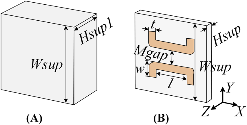
Various superstrate involved in the design process. (A) Dielectric superstrate, (B) semi-arc MS. = , = , = , w = , l = , = .
To design the MS to function as the WAIM layer, it is desired to realise the MS with a high permittivity, which effectively increases equivalent capacitance, as explained by Equation 1.where and are equivalent capacitance and permittivity of MS. and are effective area and distance decided by MS structure. According to broadband matching theory, the Bode-Fano limit can be expressed as Equation 2.where and are the centre frequency and bandwidth, respectively, the bandwidth of the TCDA array is increased with the reduction of . To clarify the properties of the 2 MS layers, the effective permeability and dielectric constant are extracted using S-parameters (Szabó et al., 2010), which are plotted in Figure 6. The proposed semi-arc MS can achieve a stable frequency response in our desired band. The of the semi-arc MS is around 4.75 and changes by around across GHz, which is higher than the pure dielectric superstrate of 2.0. According to Snell’s law, higher will contribute to profile reduction (Yu et al., 2011). Meanwhile, the of semi-arc MS is close to 1, which means the MS acts as a purely electric surface. A stable is realised across the whole band. It is noted that the value of is lower than the free space, meaning the MS acts as a low-loss impedance matching facilitator between the array and free space.
FIGURE 6
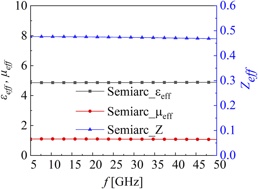
Extracted and calculated of semi-arc MS layer.
Figure 7 shows the VSWR results of the proposed TCDA unit in an infinite array when loading or without various WAIM layers. As observed in Figure 7, without any superstrate matching layer, the impedance matching is very limited, especially in the higher frequency band. After loading the dielectric superstrate, the impedance matching in the middle-frequency band is effectively enhanced, but still cannot cover the desired band. While the semi-arc MS layer can achieve good impedance matching, the latter offers the best impedance matching in the higher frequency band from 28 to 32 GHz. Meanwhile, the semi-arc MS layer can provide more benefits for scanning applications.
FIGURE 7
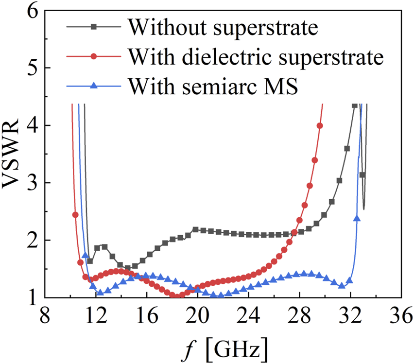
VSWR results of the proposed TCDA unit cell with or without superstrate in an infinite array.
2.4 Finite array simulation results
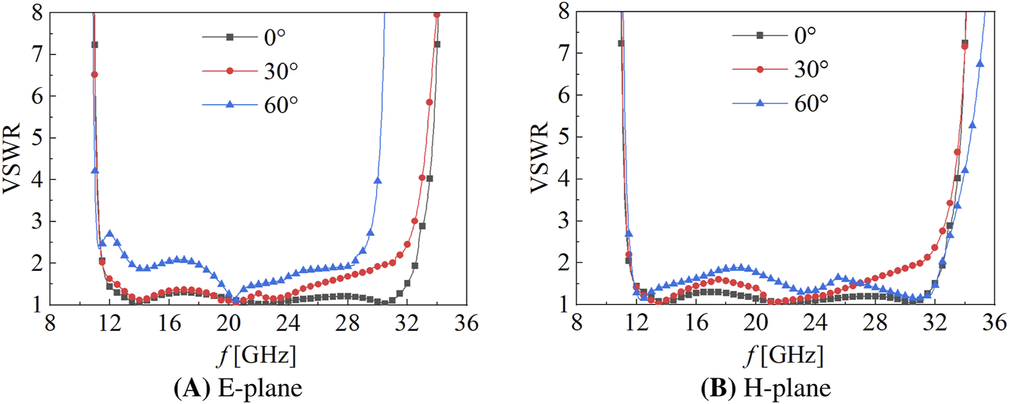
The aforementioned discussions on the designed TCDA are evaluated using the unit cell periodic boundary condition in the CST Microwave Studio. To assess the beam scanning performance and the radiation performance of the proposed TCDA in the finite array environment, as in a real application, a array is configured and simulated using the open boundary condition in the CST Microwave Studio. To mitigate the edge effect, the finite array is surrounded with the additional outer elements (as shown in the blue colour area of Figure 8), and they are set as passive elements that are terminated with loads. It is worth noting that the internal elements (as shown in the red colour area of Figure 8) are excited as active elements. The simulated results of the proposed TCDA array for E− and H-plane scanning are presented in Figure 9. As can be observed from the Figure 7, the simulated VSWR of the proposed finite TCDA is always below 1.5 from 12 to 32 GHz for broadside. In addition, the array can achieve scanning angles of up to in both E− and H-planes while maintaining a across the 12–30 GHz frequency range. To further evaluate the scanning capability of the designed array, Figure 10 indicates the simulated scanning patterns of the proposed array at 12 GHz (the lowest operating frequency), 21 GHz (the middle operating frequency), and 30 GHz (the highest operating frequency) in E− and H-planes, respectively. The radiation beam of the proposed TCDA array is scanned away from broadside to at these three frequencies, with the gain dropping by less than 3 dB in both planes. In addition, the array’s relative cross-polarisation (X-pol) levels remain below dB for all scanning angles at both planes across the considered frequencies.
FIGURE 8

Feeding topology and (B) configuration of the 7 7 array. (A) E-plane (B) H-plane.
FIGURE 9
Simulated in a finite array at (A) E-plane and (B) H-plane.
FIGURE 10
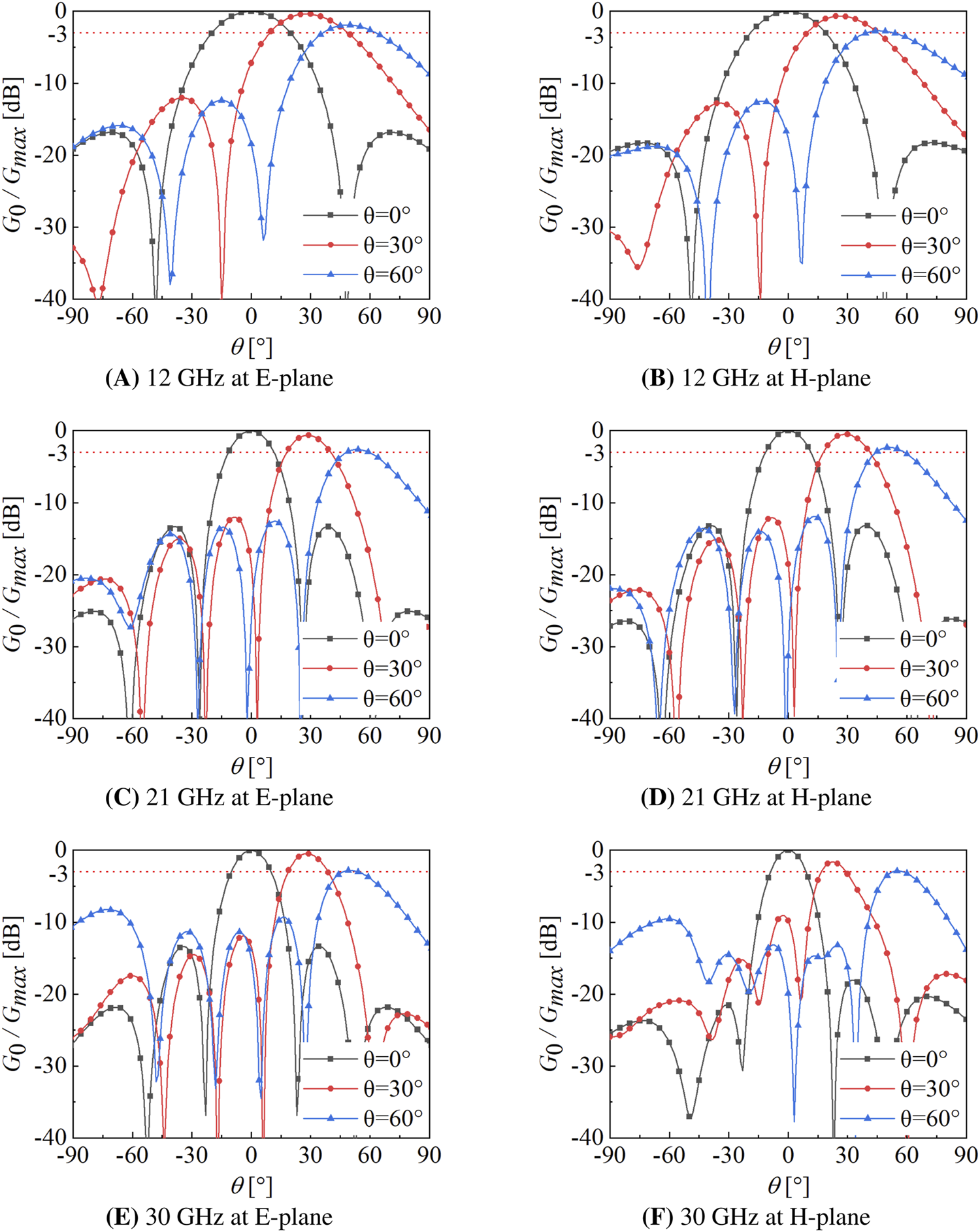
Simulated scanning radiation patterns of the array at 12 GHz, 21 GHz, and 30 GHz. (A), (C), and (E) for the E-plane, (B), (D), and (F) for the H-plane.
The gain, a crucial parameter, is frequently used to gauge the antenna performance. Detailed variations in gain at different scanning angles across both planes are meticulously detailed in Table 1 for three distinct configurations: (Case 1: E-wall with superstrate, Case 2: E-wall with semi-arc MS, and Case 3: capacitive strips with semi-arc MS). In Case 1, where the E-wall is paired with a superstrate, this configuration supports scanning angles up to at frequencies covering from 12 to 20 GHz in both planes. In addition, the integration of semi-arc MS in Case 2 notably extends the operational frequency up to 24 GHz, showcasing semi-arc MS’s capability to enhance wideband impedance matching during scanning procedures. Furthermore, replacing the E-wall with capacitive strips in Case 3 reduces common-mode interference and expands the bandwidth, signifying a substantial enhancement in antenna performance. On the other hand, the radiation efficiency remains consistently high, indicating that Case 3 does not compromise efficiency even at larger scanning angles.
TABLE 1
| Simulated realised gain at various Scanning angle | Radiation efficiency (%) | Frequency | |||||
|---|---|---|---|---|---|---|---|
| 12 GHz | 16 GHz | 20 GHz | 24 GHz | 30 GHz | |||
| (dBi) | Case 1 | 92–96 | 12.1 | 14.8 | 16.8 | / | / |
| Case 2 | 93–94 | 10.5 | 14.5 | 16.7 | 18.2 | / | |
| Case 3 | 92–94 | 12.1 | 14.8 | 17.2 | 18.4 | 20.4 | |
| (dBi) | Case 1 | 93–95 | 11.6 | 14.2 | 16.3 (E) 16.2 (H) | / | / |
| Case 2 | 91–94 | 10.0 (E)9.4 (H) | 13.9 | 16.1 (E)16.2 (H) | 17.5 (E) 17.9 (H) | / | |
| Case 3 | 92–94 | 11.6 (E)11.5 (H) | 14.3 (E) 14.2 (H) | 16.5 (E) 17.9 (H) | 17.8 (E) 17.9 (H) | 18.6 | |
| (dBi) | Case 1 | 91.5–93 | 10.2 (E) 9.8 (H) | 12.3 (E) 12.4 (H) | 13.9 (E) 14.2 (H) | / | / |
| Case 2 | 92–94 | 10.0 (E) 7.6 (H) | 11.7 (E) 12.3 (H) | 13.9 (E) 14.4 (H) | 14.8 (E) 15.9 (H) | / | |
| Case 3 | 92–93 | 9.9 (E)9.8 (H) | 12.3 (E)12.1 (H) | 14.2 (E)13.8 (H) | 15.7 (E)15.8 (H) | 17.4 (E)17.3 (H) | |
Simulated realised gain and radiation efficiency of the proposed TCDA with scanning angle at different frequencies in both planes. (case 1: E-wall with superstrate, case 2: E-wall with semi-arc MS, case 3: capacitive strips with semi-arc MS.).
The bold values are used to emphasize the performance of the proposed antenna.
3 Measurement and discussion
To verify the working principle of the proposed TCDA, the finite 5 5 array antenna with dummy elements was fabricated as shown in Figure 11. Due to the limitations of measurement conditions, only the center port was measured for VSWR, while all other ports were terminated with loads. The measured VSWR is in good agreement with the simulated one, within the frequency range of 12–30 GHz under VSWR , as displayed in Figure 12A. The realised gain of the array can also be obtained from the embedded element pattern. The simulated and measured realised gains show only a tiny deviation, less than 1 dB is observed, shown in Figure 12B, where the ideal aperture gain is also shown for reference. The disparities are mainly due to test errors and the connected cable.
FIGURE 11

Fabricated prototype of the proposed finite array.
FIGURE 12

(A) Simulated and measured VSWR results of the center element, (B) Simulated and measured realised gain of the array at broadside radiation.
Similar to the VSWR measurement, the radiation patterns of the centre element were carefully measured, showing good consistency with the simulated results, as illustrated in Figure 13. The simulated cross-polarisation patterns in the H-plane are below −40 dB, which are not shown here. It is noted that some fluctuations can be observed in the co-polarisation patterns, especially at the higher frequencies, as the array size is relatively small (Jiang et al., 2020).
FIGURE 13
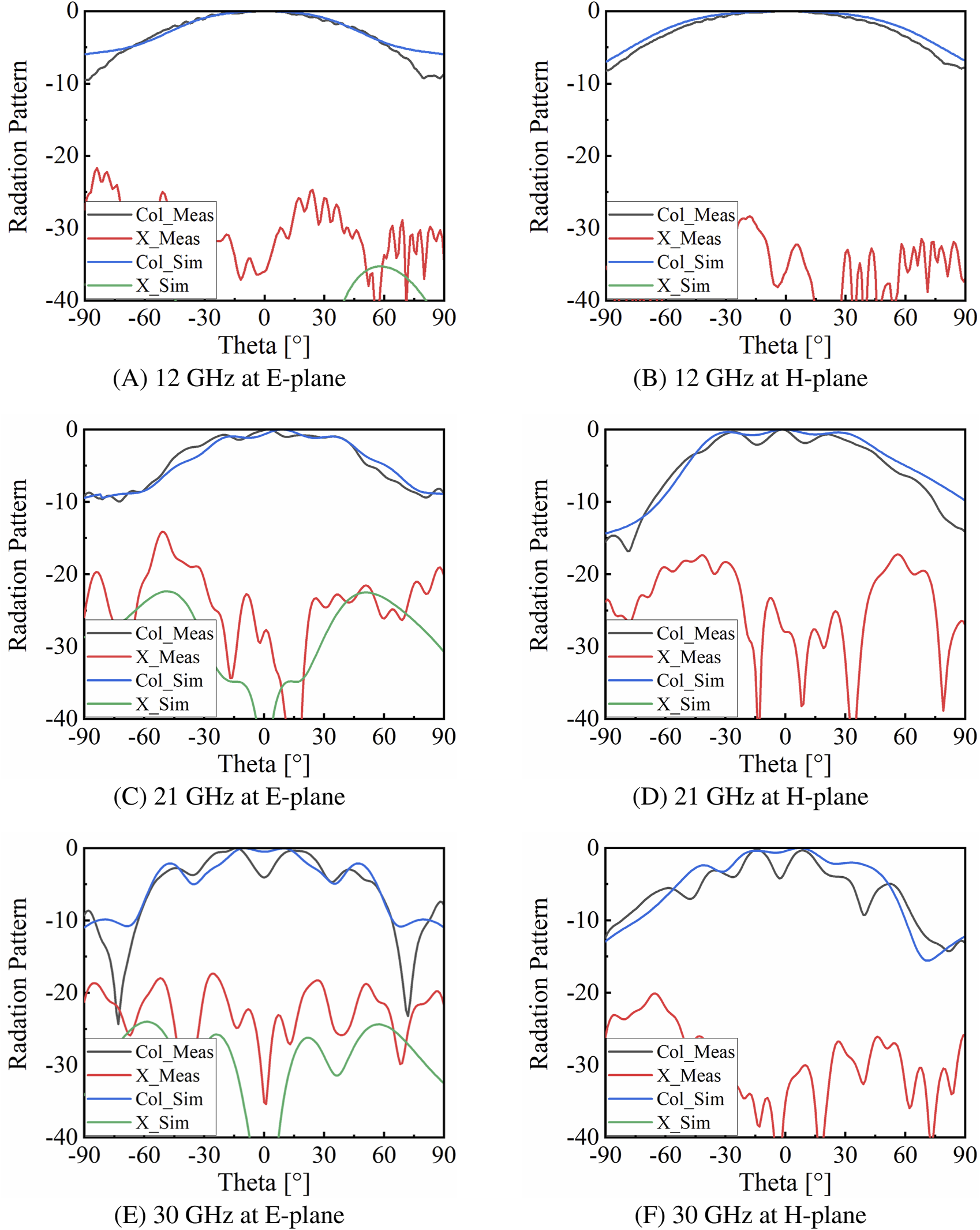
Simulated scanning radiation patterns of the array at 12 GHz, 21 GHz, and 30 GHz. (A), (C), and (E) for the E-plane, (B), (D), and (F) for the H-plane.
To highlight the advancement of the proposed TCDA array, the figure of merit has been introduced to evaluate the overall performance of the proposed design (Doane, 2013). For a lossy array, the definition of the array figure of merit can be defined as Equations 3-5.where is the maximum scan angle, is the total efficiency of the array, is the worst-case reflection coefficient. provides a single metric for a given array height, which involves engineering trade-offs between bandwidth, efficiency, and scanning angle. As can be observed from Table 2, the proposed antenna array has a higher value than existing designs reported to date, indicating that the proposed design performs better than others. Regarding scanning performance, the proposed design achieves a scan range of up to in both planes across a wide bandwidth from 12 to 30 GHz while maintaining the VSWR 2.5. This performance is notable when compared to existing designs. For instance, while similar scanning capabilities are reported in the publication Logan et al. (2017) and Liu et al. (2024), their bandwidth VSWR performances are inferior to our design, potentially resulting in higher reflection losses and degraded efficiency. From the perspective of VSWR, the designs in Shim et al. (2019) and Moghaddam et al. (2020) realise a lower VSWR but suffer from significant drawbacks: their scanning angles are reduced by half to , and they are accompanied by a higher profile, restricting their practical applicability. The latest design Kim and Nam (2024) offers a competitive profile height and high-efficiency transmission, but the scanning performance is limited to , which is narrower than that of the proposed design. Overall, the proposed design achieves a figure of merit of 0.63, calculated using Equation 3, which exceeds that of all referenced publications. This highlights the key advantage of our design: it effectively balances a broader scanning range with a reasonable VSWR while maintaining a lower profile for enhanced practical implementation. These attributes underscore the excellent performance and applicability of the proposed design.
TABLE 2
| Reference | Figure of merit | Frequency (GHz) | VSWR | Scanning angle at both planes | Element size | Array size |
|---|---|---|---|---|---|---|
| Shim et al. (2019) | 0.10 | 22.6–32.5 | 2 | up to 30° | ||
| Moghaddam et al. (2020) | 0.32 | 17–42 | 2 | up to 45° | ||
| Logan et al. (2017) | 0.53 | 3.53–21.2 | 3.9 | up to 60° | ||
| Sun et al. (2021) | 0.42 | 4–18 | 3.5 | up to 45° | ||
| Liu et al. (2024) | 0.29 | 8–18.5 | 5 | up to 60° | ||
| Kim and Nam. (2024) | 0.53 | 24.3–42.1 | 2 | up to 45° | ||
| This Work | 0.63 | 12–30 | 2.5 | up to 60° |
Comparisons between existing works and the proposed design (: the wavelength of the low frequency).
The bold values are used to emphasize the performance of the proposed antenna.
4 Conclusion
This work presents a low-profile, ultra-wideband, wide-scanning tightly coupled dipole array (TCDA) antenna, optimised for high-performance satellite and millimetre-wave communication systems. The proposed array operates across an extended frequency range of 12–30 GHz, supporting a wide-angle scanning capability up to in both E− and H-planes while maintaining a voltage standing wave ratio (VSWR) below 2.5. Notably, the design maintains a compact profile of just ( is the wavelength at the lowest operating frequency), addressing the volumetric constraints typical in mobile SATCOM platforms.
Key innovations include incorporating key implementations for enhanced array performance, e.g., using planar shorted dipole patches excited via a -shaped probe and integrating capacitive strips to suppress common-mode resonances without added structural complexity. This proposed approach reduced the fabrication complexity compared to the conventional E-wall design for TCDA, offering a lower manufacturing cost. A novel semi-arc-shaped metasurface (MS) layer with high effective permittivity is introduced as a wide-angle impedance matching (WAIM) layer, enhancing impedance matching and enabling profile reduction. This MS exhibits stable wave impedance and low dispersion, contributing to consistent broadband performance.
Simulated and measured results from a fabricated array prototype validate the design’s performance. The array achieves broadside realised gains up to 20.4 dBi at 30 GHz and maintains less than 3 dB gain degradation even at scan angles. Cross-polarisation levels remain below dB across all scanned angles. Compared to existing solutions, the design achieves a superior figure of merit , outperforming prior works in balancing bandwidth, scan angle, and physical profile.
Combining technical rigour with practical manufacturability—using low-cost Rogers RO4350B substrates in a planar configuration—establishes a new benchmark for future broadband, mobile, and low-profile phased array antennas. Its scalability and efficiency make it highly suitable for commercialised SATCOM, 6G non-terrestrial networks, and radar systems requiring agile beamforming under strict form factor constraints.
Statements
Data availability statement
The original contributions presented in the study are included in the article/supplementary material, further inquiries can be directed to the corresponding author.
Author contributions
WD: Data curation, Investigation, Methodology, Writing – review and editing, Visualization, Validation, Formal Analysis, Funding acquisition, Writing – original draft. WY: Investigation, Conceptualization, Formal Analysis, Supervision, Methodology, Writing – review and editing. AA: Investigation, Supervision, Writing – review and editing, Funding acquisition, Formal Analysis, Project administration.
Funding
The author(s) declare that financial support was received for the research and/or publication of this article. Ms. Dang Wen’s PhD project is supported by the China Scholarship Council (CSC). Additional support from the ELLIIT Strategic Research Environment (https://elliit.se/) for Andrés Alayón Glazunov is also appreciated.
Acknowledgments
WD would like to express her sincere gratitude to Dr. Qina Long, Dr. Xue Bing, and Dr. Chen Quangang for their assistance during the measurement.
Conflict of interest
Author WY was employed by Rohde & Schwarz GmbH & Company KG.
The remaining authors declare that the research was conducted in the absence of any commercial or financial relationships that could be construed as a potential conflict of interest.
Generative AI statement
The author(s) declare that no Generative AI was used in the creation of this manuscript.
Publisher’s note
All claims expressed in this article are solely those of the authors and do not necessarily represent those of their affiliated organizations, or those of the publisher, the editors and the reviewers. Any product that may be evaluated in this article, or claim that may be made by its manufacturer, is not guaranteed or endorsed by the publisher.
References
1
AnsariS.TahaA.DashtipourK.SamboY.AbbasiQ. H.ImranM. A. (2021). Urban air mobility—a 6G use case?Front. Commun. Netw.2, 729767. 10.3389/frcmn.2021.729767
2
BahA. O.QinP.-Y.ZiolkowskiR. W.GuoY. J.BirdT. S. (2019). A wideband low-profile tightly coupled antenna array with a very high figure of merit. IEEE Trans. Antennas Propag.67, 2332–2343. 10.1109/TAP.2019.2891460
3
DangW.YongW. Y.GlazunovA. A. (2022). “Ultra-wideband, wide scanning phased array for SATCOM ground station,” in 2022 international symposium on antennas and propagation (ISAP), 57–58. 10.1109/ISAP53582.2022.9998860
4
DoaneJ. P. (2013). Wideband low-profile antenna arrays: fundamental limits and practical implementations. Columbus, OH, USA: Ohio State University. Ph.d. dissertation.
5
DoaneJ. P.SertelK.VolakisJ. L. (2012). “A 6.3 : 1 bandwidth scanning tightly coupled dipole array with Co-designed compact balun,” in Proceedings of the 2012 IEEE international symposium on antennas and propagation (IEEE), 1–2.
6
DoaneJ. P.SertelK.VolakisJ. L. (2013). A wideband, wide scanning tightly coupled dipole array with integrated balun (TCDA-IB). IEEE Trans. Antennas Propag.61, 4538–4548. 10.1109/tap.2013.2267199
7
GouY.ChenY.YangS. (2024). A tightly coupled dipole array with diverse element reflection phases for RCS reduction. Chin. J. Electron.33, 449–455. 10.23919/cje.2022.00.121
8
GuX.LiuD.SadhuB. (2021). Packaging and antenna integration for silicon-based millimeter-wave phased arrays: 5g and beyond. IEEE J. Microwaves1, 123–134. 10.1109/jmw.2020.3032891
9
JiangZ.XiaoS.YaoZ.WangB.-Z. (2020). A planar ultrawideband wide-angle scanning array loaded with polarization-sensitive frequency-selective surface structure. IEEE Trans. Antennas Propag.68, 7348–7357. 10.1109/TAP.2020.2997470
10
KimS.NamS. (2024). Wideband vertically polarized endfire metasurface antenna fed by tightly coupled monopole probe array. IEEE Trans. Antennas Propag.72, 2481–2489. 10.1109/TAP.2024.3356057
11
KimY.-S.SchvartzmanD.PalmerR. D.YuT.-Y.NaiF.CurtisC. (2024). Phased array weather radar architectures for doppler estimation with space time processing. IEEE Trans. Radar Syst.2, 725–738. 10.1109/trs.2024.3444785
12
LathaT.RamG.KumarG. A.ChakravarthyM. (2021). Review on ultra-wideband phased array antennas. IEEE Access9, 129742–129755. 10.1109/access.2021.3114344
13
LeeH.NamS. (2017). A dual-polarized 1-d tightly coupled dipole array antenna. IEEE Trans. Antennas Propag.65, 4511–4518. 10.1109/TAP.2017.2723262
14
Lee HakjuneN. S.YoonM.NamS. (2019). Cylindrical tightly coupled dipole array antenna. J. Electromagn. Eng. Sci.19, 122–129. 10.26866/jees.2019.19.2.122
15
LiW.GaoS.ZhangL.LuoQ.CaiY. (2017). An ultra-wide-band tightly coupled dipole reflectarray antenna. IEEE Trans. antennas Propag.66, 533–540. 10.1109/tap.2017.2772311
16
LiM.ChenS.-L.LiuY.GuoY. J. (2023). Wide-angle beam scanning phased array antennas: a review. IEEE Open J. Antennas Propag.4, 695–712. 10.1109/ojap.2023.3296636
17
LiangX.YinW.ChenA.ZhangZ.ZengJ.ShiL.et al (2020). Ultrawideband, wide scanning stripline-fed tightly coupled array antenna based on parallel-dipole elements. Sensors20, 5065. 10.3390/s20185065
18
LindbergP.ÖjeforsE.BarnaZ.Thornell-PersA.RydbergA. (2007). Dual wideband printed dipole antenna with integrated balun. IET microwaves, antennas & Propag.1, 707–711. 10.1049/iet-map:20050286
19
LiuH.LiuJ.HuangJ.HanC.ChenB.LiuY.et al (2024). A wide-band low-profile antenna for a high-integration phased array system. Sensors24, 3295. 10.3390/s24113295
20
LoganJ. T.KindtR. W.LeeM. Y.VouvakisM. N. (2017). A new class of planar ultrawideband modular antenna arrays with improved bandwidth. IEEE Trans. Antennas Propag.66, 692–701. 10.1109/tap.2017.2780878
21
LoganJ. T.KindtR. W.VouvakisM. N. (2018a). A 1.2–12 GHz sliced notch antenna array. IEEE Trans. antennas Propag.66, 1818–1826. 10.1109/tap.2018.2809476
22
LoganJ. T.KindtR. W.VouvakisM. N. (2018b). Low cross-polarization vivaldi arrays. IEEE Trans. antennas Propag.66, 1827–1837. 10.1109/tap.2018.2809492
23
MoghaddamS. M.YangJ.ZamanA. U. (2020). Fully-planar ultrawideband tightly-coupled array (FPU-TCA) with integrated feed for wide-scanning millimeter-wave applications. IEEE Trans. Antennas Propag.68, 6591–6601. 10.1109/TAP.2020.3001448
24
MoulderW. F.SertelK.VolakisJ. L. (2013). Ultrawideband superstrate-enhanced substrate-loaded array with integrated feed. IEEE Trans. Antennas Propag.61, 5802–5807. 10.1109/tap.2013.2280001
25
MunkB. A. (2006). “A wide band low profile array of end loaded dipoles with dielectric slab compensation,”. The European conference on antennas and propagation: EuCAP 2006. Editors LacosteH.OuwehandL. (ESA Special Publication), 9.
26
MunkB. A. (2003). Theory. John Wiley Sons, Ltd, 3. 56–83. 10.1002/0471457531.ch3
27
MunkB.TaylorR.DurharnT.CroswellW.PigonB.BoozerR.et al (2003). “A low-profile broadband phased array antenna,”, 2. USNC/CNC/URSI North American Radio Sci, 448–451. 10.1109/APS.2003.1219272IEEE Antennas Propag. Soc. Int. Symposium. Dig. Held conjunction
28
PapantonisD. K.VolakisJ. L. (2015). Dual-polarized tightly coupled array with substrate loading. IEEE Antennas Wirel. Propag. Lett.15, 325–328. 10.1109/lawp.2015.2443725
29
ShimJ.-Y.GoJ.-G.ChungJ.-Y. (2019). A 1-D tightly coupled dipole array for broadband mmWave communication. IEEE Access7, 8258–8265. 10.1109/access.2018.2889333
30
SunJ. X.ChengY. J.FanY. (2021). Planar ultra-wideband and wide-scanning dual-polarized phased array with integrated coupled-marchand balun for high polarization isolation and low cross-polarization. IEEE Trans. Antennas Propag.69, 7134–7144. 10.1109/tap.2021.3060136
31
SzabóZ.ParkG.-H.HedgeR.LiE.-P. (2010). A unique extraction of metamaterial parameters based on kramers–kronig relationship. IEEE Trans. Microw. Theory Tech.58, 2646–2653. 10.1109/TMTT.2010.2065310
32
WangH.QuS.-W.YangS.HuJ. (2023). Low-profile planar ultrawideband modular antenna array loaded with parasitic metal strips. IEEE Trans. Antennas Propag.71, 5805–5816. 10.1109/TAP.2023.3277217
33
WenL.Sanz-IzquierdoB.HuW.LinC.WangC. (2024). Lightweight, low-cost, tightly coupled dipole array antenna for wireless power transfer. IEEE Antennas Wirel. Propag. Lett.23, 3797–3801. 10.1109/LAWP.2024.3390448
34
WheelerH. (1965). Simple relations derived fom a phased-array antenna made of an infinite current sheet. IEEE Trans. Antennas Propag.13, 506–514. 10.1109/TAP.1965.1138456
35
XylourisG.NomikosN.KalafatelisA.GiannopoulosA.SpantideasS.TrakadasP. (2024). Sailing into the future: technologies, challenges, and opportunities for maritime communication networks in the 6G era. Front. Commun. Netw.5, 1439529. 10.3389/frcmn.2024.1439529
36
YongW. Y.Alayón GlazunovA. (2023). Impact of dielectric substrate on the performance of an 8 × 8 magneto-electric dipole phased array antenna for 5g mmwave applications. Front. Commun. Netw.4, 1135941. 10.3389/frcmn.2023.1135941
37
YuN.GenevetP.KatsM. A.AietaF.TetienneJ.-P.CapassoF.et al (2011). Light propagation with phase discontinuities: generalized laws of reflection and refraction. science334, 333–337. 10.1126/science.1210713
38
ZhangZ.WangB.YangF.ChenY.QuS.-W.HuJ.et al (2022). Conical conformal tightly coupled dipole arrays Co-Designed with low-scattering characteristics. IEEE Trans. Antennas Propag.70, 12352–12357. 10.1109/TAP.2022.3209732
39
ZhouY.ZhuF.GaoS.LuoQ.WenL.-H.WangQ.et al (2018). Tightly coupled array antennas for ultra-wideband wireless systems. IEEE Access6, 61851–61866. 10.1109/ACCESS.2018.2873741
40
ZhouH.QuanX.CaoZ.XuZ. (2022). “A novel ultra-wideband wide-angle scanning dual-polarized antenna with multilayer dielectric. J. Phys. Conf. Ser.2387. 10.1088/1742-6596/2387/1/012006
Summary
Keywords
array antenna, high refractive index metamaterial, phased array antenna, tightly coupled dipole array antenna (TCDA), ultra-wideband (UWB), wide scanning
Citation
Dang W, Yong WY and Glazunov AA (2025) Low-profile, wideband, wide-scanning tightly coupled dipole phased array antenna. Front. Commun. Netw. 6:1613225. doi: 10.3389/frcmn.2025.1613225
Received
16 April 2025
Accepted
25 July 2025
Published
28 August 2025
Volume
6 - 2025
Edited by
Francisco Falcone, Public University of Navarre, Spain
Reviewed by
Jawad K. Ali, University of Technology, Iraq
Jianfeng Zheng, University of Houston, United States
Updates
Copyright
© 2025 Dang, Yong and Glazunov.
This is an open-access article distributed under the terms of the Creative Commons Attribution License (CC BY). The use, distribution or reproduction in other forums is permitted, provided the original author(s) and the copyright owner(s) are credited and that the original publication in this journal is cited, in accordance with accepted academic practice. No use, distribution or reproduction is permitted which does not comply with these terms.
*Correspondence: Andrés Alayón Glazunov, andres.alayon.glazunov@liu.se
Disclaimer
All claims expressed in this article are solely those of the authors and do not necessarily represent those of their affiliated organizations, or those of the publisher, the editors and the reviewers. Any product that may be evaluated in this article or claim that may be made by its manufacturer is not guaranteed or endorsed by the publisher.