- 1Department of Electronics, University of Alcalá, Alcalá de Henares, Spain
- 2Department of Technology, Centro de Investigaciones Energéticas Medioambientales y Tecnológicas (CIEMAT), Madrid, Spain
Charge-coupled devices (CCDs) play crucial roles in astronomy owing to their widespread use in the optical band, offering high sensibility, low noise, high dynamic range, and high spatial resolution. Recent advancements in CCDs have focused on improving the sub-electron noise levels for particle detection and enhancing readout speeds through simulation studies. The main objective of this study is to replace the analog processing of CCD signals using the digital-correlated double sampling (DCDS) technique. DCDS allows post-acquisition noise correction through intermittent sampling of an internal reference voltage to provide compact and flexible performance. In this study, DCDS was evaluated using two digital processing systems, namely, a 2.5 mega-samples per second (MSPS) 24-bit analog-to-digital converter (ADC) board and a 250 MSPS 16-bit ADC field-programmable-gate-array( FPGA)-based buffer memory board. The readout noise value at 74 kpix/s (7.1 e) was a significant improvement over that obtained with analog processing (9.7 e). The DCDS implementation demonstrates optimal signal-to-noise ratio for a wide range of readout speeds. Parameters such as the sample positions per pixel, number of samples, and number of pixels were identified to be essential in achieving an accurate gain value. Finally, hardware implementation of the DCDS IP core algorithm on a Xilinx Zynq-7000 AP system-on-a-chip (SoC) showed a significant improvement in power dissipation (7.1 W) compared to the analog Monsoon correlated double sample (CDS) circuit (13.6 W). The DCDS IP core implementation also showed a background noise reduction of up to 34% compared to DCDS offline readout processing using a Python algorithm.
1 Introduction
Scientific charge-coupled devices (CCDs) are currently used in various applications that require very low noise performances. CCD readouts are often implemented via correlated double sampling (CDS) using switched-capacitor circuits or digital signal processing algorithms after analog-to-digital conversion. By adjusting the interval between the clamping and sample-and-hold stages, the CDS approach can flexibly filter low-frequency noise to enhance the signal-to-noise ratio (SNR) and reduce the noisy electrons. Although CDS cancels offset and flicker noise (a type of electronic noise with a frequency spectrum that follows the 1/f law with increasing frequency in sensor signal conditioning), it requires substantial circuitry for the conversion of the received photons to digital data (Dobrev and Neycheva, 2020). CDS integration with low-noise amplifiers and analog signal processing blocks in application-specific integrated circuits (ASICs) can also contribute to noise suppression. Different approaches have been developed to optimize CCD readouts, such as specialized ASICs for CCD controllers (Juramy et al., 2014; Bessia et al., 2023) and novel analysis methods to reduce the pixel readout times (Gach et al., 2003; Moroni et al., 2020). Additionally, the use of CCDs in scientific instrumentation like telescopes underscores the importance of selecting a detector with a low readout noise (RON) and designing efficient controllers for driving the CCDs (Howell, 2000). Advancements in gamma-ray astronomy have highlighted the significance of readout electronics design, especially for detectors like photomultiplier tubes and silicon photomultipliers, emphasizing the need for integrated microelectronic implementations and different signal readout strategies (Carminati and Fiorini, 2024).
In this context, digital-correlated double sampling (DCDS) is an innovative sensor readout approach that allows low-frequency noise and offers post-acquisition noise correction through intermittent sampling of an internal reference voltage. This feature allows real-time acquisition using digital techniques for high bandwidth (Paul et al., 2022; Bourgeois et al., 2017). The present study entails a DCDS implementation system that offers a cost-effective, low-power, and digital compact solution for CCD readout, which makes it a promising technique in astronomical observations and imaging systems.
1.1 Related works
DCDS technology has been applied in astronomical cameras with mathematical models to aid with noise suppression. Several DCDS methods have been developed theoretically, whose performances have to be compared, as emphasized by Clapp (2012). Numerical simulations demonstrate the possibility of predicting the point with the lowest RON for a DCDS model, enhancing the selection of optimal parameters for noise reduction (Duan et al., 2021). For instance, Yao et al. (2023) demonstrated through simulations that noise reduction could be achieved with more sample processing. The RON in CCDs can be significantly reduced (i.e., by 4 e, requiring up to 300 sampling points at 83.3 kHz operating frequency), as highlighted by Liu et al. (2015). DCDS not only minimizes the reset noise in detectors but also provides low RON to balance the digital sampling rate against the pixel rate (Clapp et al., 2016). In this context, Clapp et al. (2017) proposed an experimental weighting method for comparisons against theoretical predictions, where the integration of transition samples does not significantly affect the gain value. DCDS has also been applied to complementary metal-oxide semiconductor (CMOS) detectors, as presented by Zou et al. (2019). The responses of specific pixel circuits at low light levels with DCDS are evaluated by subtracting the reset noise from the pixel signals off-chip. Although this approach cannot remove flicker noise completely, the column noise (a type of noise arising from mismatches in the column-parallel readout circuits of image sensors) can be reduced. The selection of timing parameters has also been evaluated for noise subtraction from video signals (Weatherill et al., 2019). Given these efforts, numerical sampling optimization is a promising method to optimize the tradeoff between the linearity and SNR of the sensor readout.
Characterization of the CCD is an essential step before its use in astronomical observations. The spectral response is a vital measure for accurately capturing and interpreting astronomical data across different wavelengths. In this regard, the significance of CCD characterization was detailed by Scuderi et al. (2023), highlighting the importance of understanding the technical specifications of CCDs before deploying them as electronic readouts. Additionally, Drlica-Wagner et al. (2020) discussed the validation of skipper CCDs by showcasing their potential to achieve stable and high quantum efficiencies as well as single-electron resolutions, which in turn refer to the detector capacity to identify and precisely measure signals generated by the absorption of individual electrons. Cruz and de Vicente (2018) underscored the critical role of detector characterization for performance optimization following the CCD photon transfer curve (PTC) method (Janesick et al., 1987; Janesick, 2007). Detectors were initially calibrated in an optical testbench and then characterized under different exposure times as CCD performances are quite sensitive to the system ground. As highlighted by Casas et al. (2014), the dark current and gain conversion factor of a CCD detector were determined in electrons per analog-to-digital unit (e/ADU) using a radioactive Fe55 source within the cryostat placed in front of the detector; this is considered an accurate test to measure the gain conversion factor. However, the emitted X-rays can also be used for a short period owing to the decay of the isotopes (half-life of 2.74 years). Jiménez et al. (2012) developed a testbench with a flat-field monochromatic light source by integrating a sphere with the ability to select different light exposure times. A data acquisition system was used to control the video bias and clock boards, the front-end electronics provided the signal distribution, and preamplifier stages were available inside the cryovessel.
Field-programmable gate array (FPGA)-readout-based processors that provide high-speed correlations based on the fast Fourier transform (FFT) (Altaf et al., 2015) or very-large-scale integration architectures using FFT (Jridi and Alfalou, 2017) have enhanced digital processing for many applications. Furthermore, multichannel single-chip correlations for photon spectroscopy based on FPGAs allow simultaneous processing of multiple input channels with high dynamic ranges (DRs) (Jakob et al., 2007; Jiang et al., 2013). These advancements showcase the power and versatility of FPGA-based systems in digital applications that require high accuracy and flexibility. For DCDS-related advances with FPGAs, Tulloch (2016) suggested using a Xilinx Spartan-3E FPGA board to implement a customized DCDS method with analog-to-digital converter (ADC) frequencies of up to 25 MHz. A differential averaging scheme with over 100 samples per pedestal pixel has been used to achieve low noise (4.2 e) at a low pixel rate (67 kpix/s). Liu et al. (2015) considered 350 effective sampling points at an operating frequency of 83.3 kHz to obtain a RON value of 44.2 e; this implementation was validated using an Fe55 radioactive source without accounting for the full-well capacity (FWC) and DR of the detector.
1.2 Research gaps
Traditional analog CDS methods suffer from thermal noise or Johnson–Nyquist noise limitations such as kT/C noise as well as settling time constraints that impact the sampling frequencies in sensing systems (Cho et al., 2023). Several researchers have explored the advantages of using digital techniques for waveform processing, given only the theoretical frameworks and simulation results (Smith and Kaye, 2013; Alessandri et al., 2015). Additionally, integrating DCDS circuits into large-area or mosaic cameras poses space and energy consumption constraints, making it difficult to implement traditional analog CDS circuits. DCDS experimental studies have also highlighted the linearity limitations occurring near clock and clock-edge transitions during sampling that can increase the total integrated noise.
1.3 Specific contributions
The main contribution of this study is the validation of innovative algorithms to analyze and process digital samples obtained from CCD readouts. Accordingly, two digital processing systems were tested over the complete DR of the CCD. Then, readout characterizations were performed based on the photon transfer (PT) method under vacuum and controlled temperature conditions to confirm the effectiveness of the digital processing approaches. However, some caveats are noted with respect to sample selection to cover the FWC by assessing both the gain (K) and RON. A customized DCDS was implemented on an FPGA, and its electronic noise accuracy was compared with that of offline DCDS. This study also reports a significant improvement in power dissipation compared to those of analog circuits; the noise values achieved were similar to those for analog processing, given the technical specifications of the CCD, demonstrating the feasibility and benefits of digital processing in the CCD readout.
The remainder of this paper is structured as follows. The CCD experimental setup and readout system capabilities are described in Section 2; Section 3 presents the DCDS technique; the characterization procedures and their results are detailed in Section 4; the DCDS implementation in IP core and its validation on an FPGA are explained in Section 5; and, finally, the discussion and conclusions of this study are presented in Sections 6, 7, respectively.
2 System description
The experimental setup was established in the clean room at Centro de Investigaciones Energéticas Medioambientales y Tecnológicas (CIEMAT), Madrid, Spain (Figure 1A) and is composed of a cryostat allowing a CCD readout. The detector used was a 200-µm-thick, fully depleted, back-illuminated device with an n-type silicon base provided by Hamamatsu Photonics Company. Then, a specific coating was developed that was sensitive in the range of 300–1,100 nm. The CCD was operated in the cooled state at 160 K after the experimental space was pumped to below 5×10⁻⁵ mbar, and these conditions were controlled using a heater. The temperature controller ensures highly stable experimental conditions and maintains the setpoint such that the fluctuations are below 1%. A minimum duration of 1 h is always required to ensure that the contaminant does not freeze onto the detector; furthermore, the experiments are commenced at least 1 h later to ensure stable operating conditions. The signals detected by the CCD were connected to a preamplifier board located inside the cryostat using a Kapton cable that was maintained at a distance of 20 cm below the CCD. This board separates the biases, clocks, and video signals, and shielding layers were included to prevent electrical coupling. Finally, single-point grounding was used to minimize the noise and ground loops as well as ensure system stability, as noted by Casas et al. (2012).
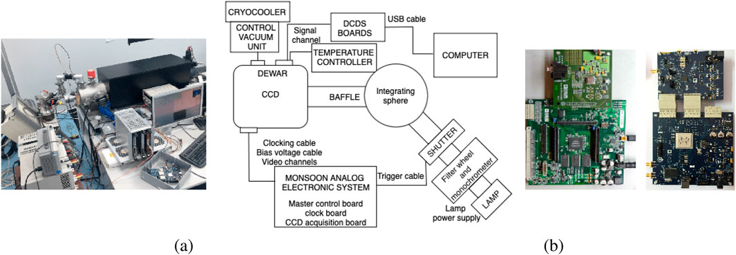
Figure 1. (A) Photograph and illustration of the experimental setup at CIEMAT; (B) electronic boards used for initial DCDS readout characterization.
The analog readout was based on the Monsoon architecture (Jiménez et al., 2016), which comprises a master control board in charge of the pixel acquisition node, an acquisition board that provides different CCD voltages, and a clock board that generates analog clocks for sequencing and shifting the burden within the CCD. Analog CCD characterization was performed by collecting image sequences with the CCD for different exposure times up to saturation. Two digital processing systems were used for the DCDS readout (Figure 1B). We also studied the impacts of oversampling using the 2.5 mega-samples per second (MSPS), 24-bit, AD7760 sigma–delta high-performance ADC board along with an Intel Altera Cyclone FPGA. The maximum internal clock frequency used is 20 MHz, and the decimation rate can be selected from the following values: 8, 16, 32, 64, 128, and 256. The pixel signals were obtained with the HSC-ADC-EVALCZ (Analog Devices, 2024), which is a high-speed converter evaluation platform that uses an FPGA-based buffer memory board to capture blocks of digital data from the AD9467; this 16-bit monolithic ADC is perfectly suitable for DCDS owing to its high conversion rate of up to 250 MHz. The memory board was connected to a personal computer via a USB port under VisualAnalog software to quickly evaluate the ADC capabilities for DCDS readout. The analog signal conditioning circuit designed with the ultralow differential amplifier ADL5562 was modified by removing the input impedance such that the input pixel signal could be increased to the full DR of the ADC. The data capture was synchronized to an external trigger that activated the three CCD readout systems for the same experimental conditions.
3 Oversampling method and DCDS readout
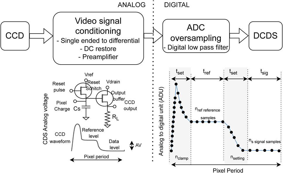
CDS reduces noise by taking two samples of the output signal, one before and one after the charge transfer, and subtracting them to cancel out the noise and offset error; it compares the reference and data levels of the CCD signals to reduce some of the noise components. The DCDS readout is usually composed of signal conditioning and oversampling processing (Figure 2). The number of ADC samples is related to the ADC frequency and system bandwidth. Furthermore, the pixels should not be sampled at the following intervals: 1) clamp period, which is the time required to restore the DC output (t is largely dependent on the system design and is commonly considered to be less than 10% of the pixel period); 2) settling period, which is the time required to stabilize the final value after a CCD charge transfer. Both these intervals are considered to be essential for ensuring accurate signal processing.
The simplest filter function is the averaging function that aims to replicate the ideal analog CDS function (Equation (1)) and requires at least two samples per pixel (i.e., reference and signal levels) to obtain the pixel value
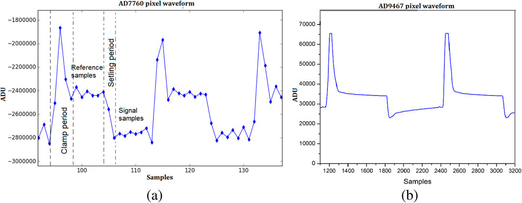
DCDS characterization was conducted using the optimal number of samples per pixel. Figure 3 shows the different readout capabilities for ADC selection. AD7760 (2.5 MSPS) achieves a maximum of 20 samples per pixel at 130 kpix/s, and AD9467 (250 MSPS) provides about 1,200 samples per pixel at 130 kpix/s. As the first step, the offline algorithms for CCD readout processing were developed and tested. Each pixel was evaluated by subtracting the reference voltage from the signal value. The absolute offset level indicates the signal measured from a region on the array where photoelectrons are not generated. For a CCD, the zero-electron level is determined by overscanning the detector’s horizontal register, where the average of the overscanned pixels represents the desired ADC offset level. For instance, the overscan pixels are virtual pixels generated by the electronics when the CCD is read, and this can be configured as extra rows of pixels to provide a measure of the electronic reference level. Hence, these pixels appear as strips along one or more sides of the CCD images, and the ADC offset is calculated as the signal from the overscan pixels that is subtracted from the signal value. The pixels must also be processed to remove samples associated with the clamp period. Figure 4 shows a part of this process by including up to 100 pixels as both the signal and overscan pixels. The clamp period was removed automatically during the preprocessing stage in the two DCDS systems.
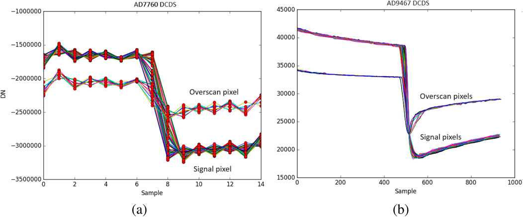
Figure 4. Signals and overscan pixels obtained at 130 kpix/s from the (A) AD7760 and (B) AD9467 systems.
4 Characterization results
According to Janesick et al. (1987), the PT method is a valuable tool for characterizing CCD imaging systems as it enables evaluation of the linearity, RON, dark current, SNR, and DR, among other parameters. The resulting pixel value S is determined using Equation (2) based on the average number of incident photons per pixel
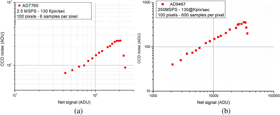
The PTC is used to determine the detector’s gain constant by converting the relative digital numbers from the detector to absolute units of electrons; this includes all data points spanning the DR from those with minimal light exposure to saturation. Typically, the exposure time is varied while maintaining the charge integration period and frame readout time constant in the PTC sequence. The noise is then calculated from the SD of the pixel values from the subarray after removing the offset value. Figure 5 shows the relationship between the CCD pixel noise and net signal, providing insights into the tradeoffs between noise and signal levels in CCD systems when using different ADCs. The CCD saturation levels were determined from the CCD noise for both DCDS systems.
Table 1 shows the K and FWC values obtained for the two readout systems compared with those for the analog Monsoon CDS. The FWCs obtained are in concordance with the values provided by the manufacturers (typically 150,000 e). The readout at 223 kpix/s was not possible from the AD7760 ADC owing to limitations. The K values obtained at 130 kpix/s for the analog CDS system, DCDS AD7760, and DCDS AD9467 were 0.46, 0.046, and 3.93 e/ADU, respectively.
Clapp et al. (2016) emphasized optimization of the weighted averaging approach and characterized the system performance using the unsettled samples within the pixel period. Considering this work as the reference, the PT method was applied along with different samples per pixel at 130 kpix/s. However, this produced an undesirable effect related to the signal level. Although the reference and signal regions are clearly differentiable from the clamp and settling periods at low signal levels, these intervals expand at high signal levels and invade the regions corresponding to the reference and signal samples. Consequently, the CCD noise increases for higher signal values.
RON was calculated from the SD of the pixels in the overscan region. Figure 6 presents performance comparisons of different readout techniques in terms of noise and gain, which are critical parameters for optimizing the CCD readout. The RON decreases as the number of samples per pixel increases, resulting in an RMS noise value of 6.26 e at 45 kpix/s, and gradually increases with readout speed. The RON obtained with the DCDS AD9467 is an improvement over that obtained with the analog Monsoon CDS system for a wide range of readout speeds. The RON obtained with the DCDS AD7760 is considerably higher at 130 kpix/s, with an out-of-scale value (285 e with K = 0.06 e/ADU) owing to the limitation of the maximum selected samples per pixel (6 samples) compared to the 700 samples per pixel selected for the AD9467. The number of samples per pixel is a crucial consideration for determining the performance at any given pixel rate, suggesting that careful control over the sampling can further influence the RON and overall system performance.
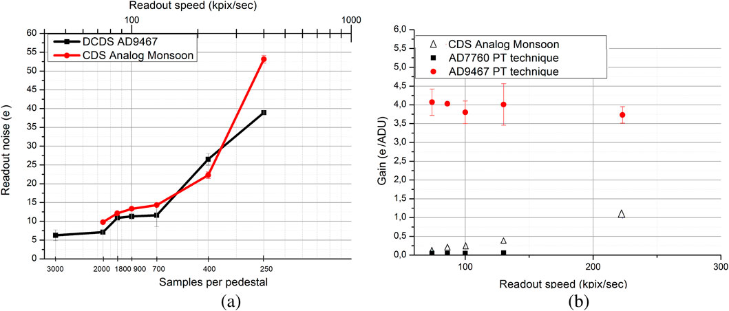
Figure 6. RON obtained from analog and DCDS AD9467 processing (A) at different readout speeds and samples per pedestal; (B) gains achieved (in e/ADU) for the two DCDS readout systems.
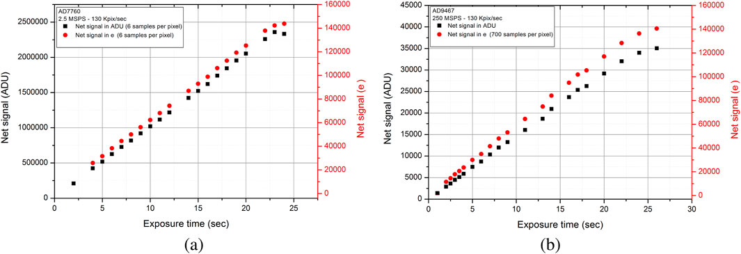
Figure 7 illustrates the net signal increases with exposure time for the two ADCs. Despite the differences in sampling rates, the net signal values in terms of electrons (red points) show similar ranges (up to 150,000 e) for both ADCs. Furthermore, saturation occurs after 25 s of exposure, demonstrating extremely good linearity. The SNR value of 19,853 (86 dB) obtained with AD9467 at 74 kpix/s was calculated as the ratio of the FWC to the RON of the detector system. The analog Monsoon CDS system provided an SNR value of 5,318 (75 dB) at the same frequency (the result was limited by the video board ADC).
The FPN is caused by the variations in charge collection from one pixel to another. Although the FPN may appear to be insignificant, with only a 1% pixel non-uniformity observed in CCD detectors, it significantly impacts the sensor’s DR and dramatically limits the signal-to-noise performance. Typically, the FPN is eliminated from images prior to data processing by subtracting consecutive images. This expands the region limited by the shot noise and enables gain calculation across the full DR of the system. The FPN is computed by subtracting the photon variance and RON from the overall noise, where
5 DCDS implementation on an FPGA
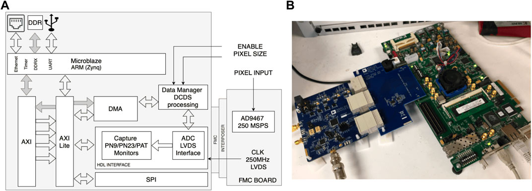
Previously, DCDS characterizations were conducted using offline DCDS Python algorithms involving analysis after data collection. In this section , we propose the implementation of real-time DCDS, where the data are instantaneously processed during acquisition. This approach enables immediate noise reduction and error correction, thereby enhancing the accuracy and quality of the results in real time. In this regard, the DCDS was implemented on a versatile and powerful platform that allows both high-performance processing and customized hardware acceleration. The Zynq-7000 FPGA system-on-a-chip (SoC) device from AMD Xilinx ZC706 (Xilinx, 2024) combines a dual-core ARM Cortex-A9 processing system with Xilinx programmable logic and is tightly integrated on a single device. Figure 8 illustrates the block diagram of the data acquisition and processing system as well as the electronic board used for the DCDS implementation.
The DCDS system is built around a customized hardware data manager IP core (Figure 9A). The algorithm offers great flexibility for weighting the ADC samples on each pedestal based on the input frequency of the DCDS signal. The operating mode of the IP core can be controlled with the clock ADC and three external signals, namely, the enable signal that initiates the CCD row, pixel size, and DCDS signals that provide the pixel rate information. The IP core module defines the ADC sample operating mode in the pixel region of interest; the samples captured in the reference region operate in the up-accumulator mode, while the samples captured in the signal region operate in the down-accumulator mode. The resulting values are then divided by the number of samples in the signal region. The operations are performed during the clamp period, and the results are output after 30 ADC clock cycles. At the end of the signal region, the final pixel value is transmitted via direct memory access (DMA) to the DDR memory. The DCDS post-implementation FPGA design and usage of FPGA resources are shown in Figure 9B. Less than 10% of the Zynq resources are used in the implementation, ensuring that the hardware design fits comfortably within the selected FPGA. The behaviors of the different IP cores comprising the DCDS readout were tested through simulations using the Vivado-integrated testbench. The final step was to provide a synthetic CCD video waveform for verification.
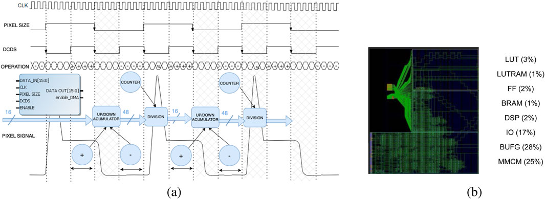
Figure 9. (A) Design of the DCDS algorithm implemented in the IP core hardware module and (B) hardware resources used in the Zynq-7000 FPGA board.
Figure 10A compares the different readout techniques and corresponding noise performances for the generated images. As examples, an image of the entire CCD under analog readout and a small CCD pixel size under DCDS readout are presented. Figure 10B shows a further comparison of the noise performances of a Python-based offline DCDS algorithm and the hardware-based DCDS implementation. To analyze the two methodologies, the same number of pixels from the overscan region were selected for each method, and the noise performances were evaluated by calculating the standard deviation of the selected pixels. The offline DCDS Python algorithm shows a higher noise characteristic (
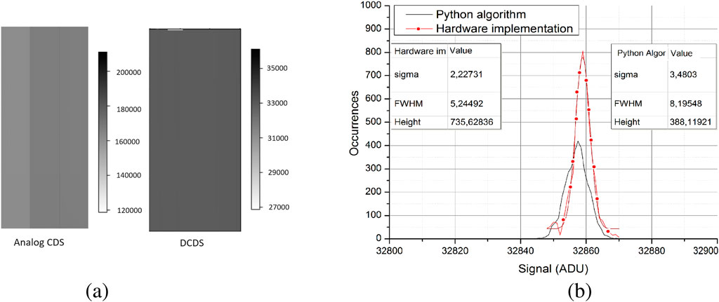
Figure 10. Images obtained with the analog Monsoon readout system (three channels) and AD9467 DCDS (A) for a specified exposure time and (B) noise comparisons between the IP core of the DCDS hardware implementation and Python offline DCDS algorithm.
Finally, according to the Monsoon report, the power dissipation for the analog Monsoon acquisition board with 12 channels states a is 25.1 W
6 Discussion
Developing an effective DCDS algorithm requires a thorough understanding of both the signal characteristics and noise sources, which adds complexity to the readout system design. According to the dataset of the Teledyne E2V CCD used in this study (Photonics, 2024), it is possible to achieve a noise level of approximately 4 e at 50 kpix/s. The results obtained for the AD9467 DCDS and Monsoon analog readout systems at 74 kpix/s (7.1 e and 9.7 e, respectively) during characterization approach this value. The use of low-power operational transconductance amplifiers and power scaling capabilities allow further optimization of the performances of the signal acquisition amplifiers, which are mainly developed for analog CDS readouts (Coln and Mueck, 2020). In our research, the noise observed at low frequencies is attributable to an issue with the preamplifier’s bandwidth, which does not allow adequate responses at these frequency levels. This work experimentally demonstrates that the “weighted samples” method can significantly reduce the RON at low signal levels. Concurrently, research on the design of low-noise differential preamplifiers or even an ASIC preamplifier that can be mounted next to the detector also offers significant advantages for developing low-noise systems. DCDS readout systems have been shown to offer optimal strategies for selecting CDS timings, highlighting the linearity of the operations and their impacts on the final pixel values (Weatherill et al., 2019). However, many studies still aim to suppress flicker noise in the CCDs using special methods that require experimental validation (Stefanov, 2015).
7 Conclusion
Although CDS techniques have shown significant promise in reducing RON, challenges remain in balancing noise suppression with system complexity and power efficiency, particularly for high-density applications. Advancements in DCDS approaches have emerged as solutions to the limitations of traditional analog methods, particularly in large-scale systems. DCDS offers enhanced capabilities through real-time processing, greater flexibility, and improved precision, thereby overcoming many limitations of the traditional analog CDS implementations.
In this study, the challenge of optimizing the CCD readout was addressed by implementing advanced hardware and digital processing techniques. The goal was to validate innovative algorithms by analyzing and processing the digital samples obtained from CCD readings and explore the potential of digital processing for enhancing performance. To this end, a hardware system was developed for implementing the DCDS technique and was characterized across the full DR of the CCD. This system was built using a 16-bit ADC with a high sample rate of 250 MSPS, which provided significant improvements over a slower 24-bit ADC operating at 2.5 MSPS. As the number of samples per pixel increased, the RON decreased, which resulted in a minimal RMS noise level of 6.26 e at 45 kpix/s for the AD9467 system. These results show noise level improvements (9.7 e) achieved with analog processing at equivalent readout speeds. The PT method was crucial in assessing the performance of the DCDS readout. The experimental results indicate that the number of samples per pixel, their positions within the pixel readout cycle, and the pattern noise factor are essential parameters for achieving accurate K values. It is also noted that high signal levels can introduce difficulties, such as expanded transition regions and unreliable PT parameters, due to unwanted transition samples in the reference and/or signal regions.
Finally, the DCDS technique was designed around a customized hardware data manager IP core, offering great flexibility for weighting the ADC samples on each pixel pedestal. A real-time DCDS CCD readout system implemented using a Zynq FPGA demonstrated improved noise performance (
Data availability statement
The original contributions presented in this study are included in the article/supplementary material; further inquiries can be directed to the corresponding author.
Author contributions
CC: conceptualization, data curation, formal analysis, investigation, methodology, resources, software, validation, visualization, writing–original draft, and writing–review and editing. JD: conceptualization, funding acquisition, investigation, project administration, supervision, validation, and writing–review and editing.
Funding
The authors declare that financial support was received for the research, authorship, and/or publication of this article. The research leading to these results were supported by Comunidad de Madrid undergrants (SPACETEC-CM S2013 ICE-2822, MINECO FPA2015-68048) and Centro de Excelencia Maria de Maeztu (MDM-2015-0509).
Conflict of interest
The authors declare that the research was conducted in the absence of any commercial or financial relationships that could be construed as a potential conflict of interest.
Publisher’s note
All claims expressed in this article are solely those of the authors and do not necessarily represent those of their affiliated organizations or those of the publisher, editors, and reviewers. Any product that may be evaluated in this article or claim that may be made by its manufacturer is not guaranteed or endorsed by the publisher.
Abbreviations
ASIC, application-specific integrated circuit; CCD, charge-coupled device; SNR, signal-to-noise ratio; DCDS, digital-correlated double sampling; FFT, fast Fourier transform; PT, photon transfer; RMS, root mean square; PTC, photon transfer curve; FWC, full-well capacity; RON, readout noise; FPN, fixed-pattern noise; DR, dynamic range; MSPS, mega-samples per second; FPGA, field-programmable gate array; CDS, correlated double sampling.
References
Alessandri, C., Abusleme, A., Guzman, D., Passalacqua, I., Alvarez-Fontecilla, E., and Guarini, M. (2015). Optimal CCD readout by digital correlated double sampling. Mon. Notices R. Astronomical Soc. 455, 1443–1450. doi:10.1093/mnras/stv2410
Altaf, M. M., Ahmad, E. H., Li, W., Zhang, H., Li, G., and Yuan, C. (2015). An ultra-high-speed fpga based digital correlation processor. IEICE Electron. Express 12, 20150214. doi:10.1587/elex.12.20150214
Analog Devices, (2024). High speed converter evaluation platform. Available at: https://www.analog.com/media/en/technical-documentation/evaluation-documentation/265181843HSC_ADC_EVALC.pdf (Accessed April 10, 2024).
Bessia, F. A., England, T., Sun, H., Stefanazzi, L., Braga, D., Haro, M. S., et al. (2023). A sub-electron-noise multi-channel cryogenic skipper-ccd readout asic. IEEE Trans. Circuits Syst. I Regul. Pap. 70, 2306–2316. doi:10.1109/tcsi.2023.3256860
Bourgeois, P.-Y., Goavec-Merou, G., Friedt, J.-M., and Rubiola, E. (2017). “A fully-digital realtime soc fpga based phase noise analyzer with cross-correlation,” in 2017 Joint conference of the European frequency and time forum and IEEE international frequency control symposium (EFTF/IFCS) (IEEE), 578–582. doi:10.1109/fcs.2017.8088963
Carminati, M., and Fiorini, C. (2024). “Readout electronics for gamma-ray astronomy,” in Handbook of X-ray and gamma-ray astrophysics (Springer), 1851–1873. doi:10.1007/978-981-19-6960-7_51
Casas, R., Ballester, O., Cardiel-Sas, L., Castilla, J., Jiménez, J., Maiorino, M., et al. (2012). Pau camera: detectors characterization. High Energy Opt. Infrared Detect. Astronomy V (SPIE) 8453, 650–657. doi:10.1117/12.924640
Casas, R., Cardiel-Sas, L., Castander, F. J., Jiménez, J., and de Vicente, J. (2014). Testing fully depleted ccd. SPIE Proc. 9147, 91472R–91967R. doi:10.1117/12.2054717
Cho, J., Choo, H., Lee, S., Yoon, S., Kam, G., and Kim, S. (2023). Design of a cmos image sensor with bi-directional gamma-corrected digital-correlated double sampling. Sensors 23, 1031. doi:10.3390/s23021031
Clapp, M. (2012). Development of a test system for the characterisation of dcds ccd readout techniques. SPIE Proc. 8453, 84531D–85430D. doi:10.1117/12.925393
Clapp, M., Mihalcea, I., Morse, T., Salter, M., and Waltham, N. (2016). Dcds weighted averaging theory and development for improved noise filtering in scientific ccd applications. SPIE Proc. 9915, 99151S–99616S. doi:10.1117/12.2231619
Clapp, M., Patel, G., Waltham, N., Hayes-Thakore, C., and Salter, M. (2017). Development of digital correlated double sampling (dcds) camera electronics for the space-based world space observatory ultra-violet spectrograph mission. Int. Conf. Space Optics—ICSO 2016 (SPIE) 10562, 142–1560. doi:10.1117/12.2296146
[Dataset] Coln, M. C., and Mueck, M. (2020). Correlated double sampling amplifier for low power. U. S. Pat. 10 (809), 792.
Cruz, C., and de Vicente, J. (2018). Digital correlated double sampling ccd readout characterization. High Energy, Opt. Infrared Detect. Astronomy VIII (SPIE) 10709, 504–512. doi:10.1117/12.2312498
Dobrev, D. P., and Neycheva, T. D. (2020). “Correlated multiple sampling techniques for sensor signal conditioning,” in 2020 XXIX international scientific conference electronics ET (IEEE), 1–4. doi:10.1109/et50336.2020.9238159
Drlica-Wagner, A., Marrufo Villalpando, E., O’Neil, J., Estrada, J., Holland, S., Kurinsky, N., et al. (2020). “Characterization of skipper ccds for cosmological applications,” in X-ray, optical, and infrared detectors for astronomy IX. Editors A. D. Holland, and J. Beletic (SPIE). doi:10.1117/12.2562403
Duan, W., Song, Q., Wei, M.-Z., Zhao, Z.-W., Wang, W., Zhang, Y.-H., et al. (2021). Research on the readout noise suppression method for digital correlated double sampling. Res. Astronomy Astrophysics 21, 013. doi:10.1088/1674-4527/21/1/13
Gach, J.-L., Darson, D., Guillaume, C., Goillandeau, M., Cavadore, C., Balard, P., et al. (2003). A new digital ccd readout technique for ultra–low-noise ccds. Publ. Astronomical Soc. Pac. 115, 1068–1071. doi:10.1086/377082
Jakob, C., Schwarzbacher, A. T., Hoppe, B., and Peters, R. (2007). “A fpga optimised digital real-time mutichannel correlator architecture,” in 10th euromicro conference on digital system design architectures, methods and tools (DSD 2007) (IEEE), 35–42. doi:10.1109/dsd.2007.4341447
Janesick, J. R., Elliott, T., Collins, S., Blouke, M. M., and Freeman, J. (1987). Scientific charge-coupled devices. Opt. Eng. 26, 692–714. doi:10.1117/12.7974139
Jiang, H. Y., Ma, Y. L., and Zhang, L. (2013). The digital correlator based on fpga in pcs. Proc. 2013 Int. Conf. Adv. Comput. Sci. Electron. Inf. doi:10.2991/ICACSEI.2013.66
Jiménez, J., Ballester, O., Cardiel-Sas, L., Casas, R., Castilla, J., Grañena, F., et al. (2012). Test benches facilities for paucam: ccds and filters characterization. SPIE Proc. 8446, 84466N–91971N. doi:10.1117/12.924883
Jiménez, J., Illa, J. M., Cardiel-Sas, L., de Vicente, J., Castilla, J., and Casas, R. (2016). The paucam readout electronics system. Ground-based Airborne Instrum. Astronomy VI (SPIE) 9908, 1443–1449.
Jridi, M., and Alfalou, A. (2017). Fpga design of correlation-based pattern recognition. SPIE Proc. 10203, 102030N–102153N. doi:10.1117/12.2264715
Juramy, C., Antilogus, P., Bailly, P., Baumont, S., Dhellot, M., El Berni, M., et al. (2014). Driving a ccd with two asics: cabac and aspic. SPIE Proc. 9154, 91541P–91556P. doi:10.1117/12.2055175
Liu, X.-Y., Lu, J.-B., Yang, Y.-J., Lu, B., Wang, Y.-S., Xu, Y.-P., et al. (2015). A digital cds technique and its performance testing. Chin. Phys. C 39, 076101. doi:10.1088/1674-1137/39/7/076101
Moroni, G. F., Chierchie, F., Stefanazzi, L., Paolini, E. E., Haro, M. S., Cancelo, G., et al. (2020). Interleaved readout of charge-coupled devices (ccds) for correlated noise reduction. IEEE Trans. Instrum. Meas. 69, 7580–7587. doi:10.1109/tim.2020.2980461
Paul, A., Fowler, P., Xu, Y., Lee, M., Wang, J., and Cauwenberghs, G. (2022). “Neural recording analog front-end noise reduction with digital correlated double sampling,” in 2022 IEEE biomedical circuits and systems conference BioCAS (IEEE), 149–152. doi:10.1109/biocas54905.2022.9948618
Photonics, H. (2024). Teledyne e2v ccd. delivery specification sheet. Available at: https://www.ing.iac.es/∼eng/detectors/K34-B72037_DeliverySpecificationSheet.pdf#:∼:text=Back%20Illuminated%20FFT-CCD%20Doc.%20No (Accessed April 10, 2024).
Scuderi, S., Bonanno, G., Bruno, P., Cali, A., and Cosentino, R. (2023). Oig and sarg ccd’s characterization. arXiv Prepr. arXiv:2302.10546. doi:10.48550/arXiv.2302.10546
Smith, R., and Kaye, S. (2013). Digital correlated double sampling for ztf. Proc. SDW2013. doi:10.1117/12.2232393
Stefanov, K. (2015). Digital cds for image sensors with dominant white and 1/f noise. J. Instrum. 10, P04003. doi:10.1088/1748-0221/10/04/p04003
Tulloch, S. (2016). Implementation of an fpga-based dcds video processor for ccd imaging. SPIE Proc. 9915, 991530–991980. doi:10.1117/12.2240405
Weatherill, D. P., Shipsey, I., Arndt, K., Plackett, R., Wood, D., Metodiev, K., et al. (2019). Automatic selection of correlated double sampling timing parameters. J. Astronomical Telesc. Instrum. Syst. 5, 1. doi:10.1117/1.jatis.5.4.041502
Xilinx, A. (2024). Zynq-7000 soc zc706 evaluation kit. Available at: https://www.xilinx.com/publications/prod_mktg/Zynq_ZC706_Prod_Brief.pdf (Accessed April 10, 2024).
Yao, D., Luo, J., Bu, F., Wen, Y., Yang, Y., Cao, W., et al. (2023). Simulation research on ccd noise reduction algorithm based on digital correlation double sampling. Third Int. Conf. Opt. Image Process. (ICOIP 2023) (SPIE) 12747, 447–453. doi:10.1117/12.2689203
Keywords: charge-coupled device, image sensor, dynamic range, digital-correlated double sampling, readout noise, gain, photon transfer function, field-programmable gate array
Citation: Cruz C and De Vicente J (2024) Charge-coupled device readout by digital-correlated double sampling. Front. Detect. Sci. Technol 2:1487623. doi: 10.3389/fdest.2024.1487623
Received: 28 August 2024; Accepted: 15 October 2024;
Published: 13 November 2024.
Edited by:
Luca Fiorini, University of Valencia, SpainReviewed by:
Fernando Carrio Argos, University of Valencia, SpainMaksym Teklishyn, Helmholtz Association of German Research Centres (HZ), Germany
Copyright © 2024 Cruz and De Vicente. This is an open-access article distributed under the terms of the Creative Commons Attribution License (CC BY). The use, distribution or reproduction in other forums is permitted, provided the original author(s) and the copyright owner(s) are credited and that the original publication in this journal is cited, in accordance with accepted academic practice. No use, distribution or reproduction is permitted which does not comply with these terms.
*Correspondence: Carlos Cruz, Y2FybG9zLmNydXp0QHVhaC5lcw==
 Carlos Cruz
 Juan De Vicente