 A. Ascoli
 N. Schmitt
 I. Messaris
 A. S. Demirkol
 R. Tetzlaff
 L. O. Chua
- 1Institute of Circuits and Systems, Faculty of Electrical and Computer Engineering, Technische Universität Dresden, Dresden, Germany
- 2Department of Electrical Engineering and Computer Sciences, University of California, Berlekey, Berkeley, CA, United States
Memristive devices are the subject of extensive studies nowadays. While the Dynamic Route Map is a powerful tool for analyzing the response of first-order memristors under DC stimuli, the development of an equivalent tool for investigating the response of these devices to AC stimuli is still an open question. Recently, Pershin and Slipko introduced a graphic method, which we name Time Average State Dynamic Route (TA-SDR), applicable to study first-order memristors subject to periodic rectangular pulse train-based stimuli. In this paper we introduce an alternative investigation tool, referred to as State Change Per Cycle Map (SCPCM), which is applicable in these very same scenarios. The novel analysis technique, inspired by the work of the French mathematician Henri Poincaré, reduces the investigation of a first-order non-autonomous continuous-time system to a simpler study of a first-order discrete-time map. A State Change Per Cycle Map defines precisely how the stimulus modulates each of the admissible device memory states over one input cycle. It is derivable either by means of numerical simulations, where a model for the ReRAM cell is available, or experimentally, in the case where the device memory state is accessible. While the predictive capability of a TA-SDR is limited to those case studies, where the AC periodic voltage signal applied across the device induces negligible changes in the respective memory state over each cycle, the conclusions drawn by analyzing a SCPCM have general validity, irrespective of the properties of the stimulus. The advantages of the novel analysis method for periodically driven ReRAM cells over the classical TA-SDR tool are highlighted through a number of case studies, some of which reveal the interesting capability of the ReRAM cell to display multiple oscillatory operating modes upon periodic stimulation via trains with a suitable number of SET and RESET pulses per period.
1 Introduction
Over the past few years, in view of a probable and inevitable impending end of the Moore era, the scientific community has been focusing with ever-growing fervor on the exploration of novel device and data processing concepts to enable sustainable progress in integrated circuit (IC) design in the years to come, especially when shrinking CMOS transistor dimensions shall no longer represent a viable option. Among the various alternatives, disruptive two-terminal nano-devices, generally called memory-resistors, or memristors (Chua, 2018) for short, in which the resistance depends upon at least one state variable, have caught the eye of the international scientific community for their potential to enable a revolutionary paradigm shift in the operating principles of computing machines (Zhang et al., 2020), which, mimicking the behavior of energy-efficient biological neural networks, may potentially outperform state-of-the-art data processing structures that suffer from the well-known limitations of classical von-Neumann architecture. With their unique capability to combine multiple functionalities within a single nanoscale physical volume, non-volatile memristors may be alternatively used to perform a calculation, including the measurement of a signal under monitoring, or to store data, which allows the hardware implementation of innovative area-, time-, and energy-efficient information management paradigms for Artificial Intelligence (AI) applications, e.g., in-memory-sensing and in-memory-computing, but cannot be run nowadays on conventional computing structures, which are fabricated purely using Complementary Metal Oxide Semiconductor (CMOS) technology.
Memristors from the non-volatile class (Ielmini and Waser, 2016) may be programmed at significantly high rates as many times as state-of-the-art high-performance data storage units, consuming very little power while switching between distinct resistance levels and retaining information encoded in some state, under zero input, for a very long time; as required in practical applications nowadays. Furthermore, while densely packed across crossbar arrays, stacked on top of standard CMOS circuitry by exploiting the natural availability of metal-insulator-metal layers along the third dimension in IC fabrication processes, they allow efficient use of the available area, endowing the resulting hybrid hardware platforms with add-on capabilities as compared to conventional technical systems. For example, non-volatile memristors enable the processing elements of standard cellular dynamic arrays to perform memory operations without the need for additional data storage units (Ascoli et al., 2021b).Interestingly, memristors may do much more. Certain resistance switching memories (Ascoli et al., 2021a), unable to store data, are attracting an increasing interest in both academia and industry for their extraordinary capability to act as sources of infinitesimal energy under suitable polarization, analogous to the ion channels in biological neuronal membranes. The adoption of these volatile memristor realizations in circuit and system design opens the opportunity to synthesize Cellular Neural Networks (CNNs) (Ascoli et al., 2022b; Ascoli et al., 2022c), mimicking closely biological systems, which may enable a better understanding of their complex bifurcation phenomena, as well as the design of ground-breaking computing machines, including spike-based computing Cellular Automata (CAs) (Pickett and Williams, 2013), which, operating according to bio-inspired principles, promise to approach the information management efficiency of the human brain. Given the potential of memristors for the electronics of the future, endowing the circuit designer’s toolkit with predictive yet simple models of non-volatile and volatile memristors, while facilitating the accessibility of the general community to their physical realizations, which would allow their usability in academic lab environments, is crucially necessary for advancement of the knowledge base, which would ultimately convince industry partners to invest massively in memristive nanotechnologies.
In parallel to modelling activities, another fundamental area of research regards the development of system-theoretic analysis techniques for exploration of the complex dynamics of these intrinsically nonlinear nano-devices. While the Dynamic Route Map1 (DRM) (Chua, 2018) is a reference graphic tool for studying the response of first-order memristors to DC excitations, an equivalent methodology for investigating its behavior under AC stimuli is not yet available.
In (Pershin and Slipko, 2019a), Pershin and Slipko studied the time evolution of the mean value of the memory state of a non-volatile Resistive Random Access Memory (ReRAM) cell (Yang et al., 2010), manufactured at Hewlett Packard (HP) Labs, under appropriately weak AC periodic rectangular pulse-based stimulation, by applying a time averaging-based approximation (Strogatz, 2015) of its mathematical description (Strachan et al., 2013). The application of this method—see also (Pershin and Slipko, 2019b) for more details—resulted in the introduction of a powerful graphic tool, enabling to infer that the level around which the memory state, initiated from a predefined initial condition, would be found to oscillate asymptotically. Here, we coin the name Time Average State Dynamic Route (TA-SDR) for such a precious analysis tool. The time averaging methodology has been recently adopted in (Messaris et al., 2023) to study the response of the aforementioned ReRAM cell to high-frequency AC periodic stimuli, which resulted in the introduction of a new strategy for programming its memory content.
In this paper, we introduce a new valuable graphic tool, which we name State Change Per Cycle Map, SCPCM for short, inspired by the Poincaré Map technique (Ascoli et al., 2005), enabling the exploration of the response of a second-order continuous-time system, corresponding to a resistance switching memory cell with scalar state variables under periodic forcing, through the simpler study of a one-dimensional discrete-time system. The derivation of a SCPCM calls for the acquirement of a data series. Each recording, which requires the run of an experiment, in the case where accessibility to the device memory state is possible, or a numerical simulation where a reliable model for the ReRAM cell is available, quantitatively defines the change in the device memory state from a prescribed initial condition over one input cycle. Spacing the initial conditions uniformly across the admissible range and then plotting each of the recordings versus the respective initial condition, a map is finally obtained by means of a suitable interpolation method. Remarkably, each fixed point of this one-dimensional discrete-time system, i.e., the abscissa of any crossing of the graph of the SCPCM with the horizontal axis, indicating an initial condition, which the stimulus maps onto itself from cycle to cycle, corresponds to a possible oscillatory mode for the periodically driven ReRAM cell. The oscillatory solution for the device memory state is then asymptotically stable (unstable) if the slope of the graph of the SCPCM is found to be negative (positive) at the fixed point under focus.
While the predictive capability of a TA-SDR is restricted to those case studies in which the amplitude and frequency of the input signal stimulating the ReRAM cell are set in such a way to induce small changes in its memory state over each cycle2, a SCPCM has general applicability, irrespective of the characteristics of the excitation signal. This paper introduces the fundamentals of the novel system-theoretic method for the investigation of first-order ReRAM cells under periodic excitation, highlighting its advantages over the standard TA-SDR graphic tool through a number of illustrative examples, some of which unveil the interesting capability of the ReRAM cell to exhibit multiple steady-state oscillatory behaviors under the application of pulse trains featuring a suitable number of pulses per cycle between its terminals.
With regard to the structure of the manuscript, a brief review of the Strachan model, capturing the nonlinear dynamics of the ReRAM cell from HP Labs, and constituting the object of the investigations in this research study, is provided in section 2. The novel system-theoretic method for exploring the response of a first-order memristor to periodic excitations is presented in section 3, which begins with a short introduction to the classical technique introduced by Pershin and Slipko for the same purpose, revolving around a time averaging-based approximation of the Strachan model. Section 4 derives the SCPCM and the TA-SDR for a number of ReRAM cell excitation scenarios, comparing their predictions, which clearly reveals the superior capability of the proposed analysis tool. Conclusions are finally drafted in section 5.
2 Memristor model
The memristor model under study was first developed by Strachan et al. (Strachan et al., 2013) in 2013 to capture the nonlinear dynamics of a ReRAM cell (Yang et al., 2010) manufactured at HP Labs and composed of a nearly stoichiometric tantalum oxide Ta2O5−x thin film sandwiched between two metal electrodes, one made of tantalum (Ta) and one of platinum (Pt). Strachan modelled this nano-device as a first-order voltage-controlled extended memristor (Chua, 2018) with the DAE set.
where a dot over a variable denotes its time differentiation, while v (i) stands for the voltage (current) falling between (flowing through) its terminals, whereas x represents the memory state variable, which is physically associated to the most conductive volume fraction of the Ta2O5−x film, being tunable, by means of stimulation, across a limited, closed range referred to as its existence domain
Here, the adoption of the Heaviside function step (⋅) allows to capture the asymmetry between the SET and RESET resistance switching dynamics. In fact, with p = i ⋅ v denoting the instantaneous power dissipated in the memristor while it is subject to some excitation, the state evolution function g (x, v) reduces either to the form
during a SET transition, i.e., for v > 0V, or to the form
during a RESET transition4, i.e., for v < 0V. Eq. 2 models the electronic transport across the nano-structure. Here G (x, v), standing for the memductance function, is expressed by
The values of the parameters in Strachan model Equations 6 and 4, and 5 (Strachan et al., 2013), as fitted to the Ta2O5−x memristor nano-device under focus here (Ascoli et al., 2016c), are listed in Table 1.
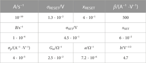
TABLE 1. Values assigned to the parameters in the Strachan DAE set (Strachan et al., 2013) so as to match the static and dynamic properties of a Ta2O5−x resistance switching memory from HP Labs (Ascoli et al., 2016c).
Back in 2016, powerful circuit- and system-theoretic methods applied to the Strachan model enabled to uncover a previously unknown dynamical phenomenon (Ascoli et al., 2016c) emerging in the nano-structure under both DC and AC periodic excitations, known5 as Fading Memory (Boyd and Chua, 1985), and explored extensively in the literature since then, e.g., in (Messaris et al., 2023) and, earlier, in (Ascoli et al., 2018) as well as in (Ascoli et al., 2022a).
3 Exploring the nonlinear dynamics of periodically-driven memristors
While an accurate graphic tool, namely, the DRM (Chua, 2018), was conceptualized for studying the response of first-order memristors to DC inputs, there is no homologous method for exploring the nonlinear behavior of these devices under AC stimuli. Under the assumption that, over each T-long cycle, a voltage signal applied across the aforementioned ReRAM cell (Yang et al., 2010) from HP Labs is null for most of the time, except within two brief temporal intervals of duration τ+ and τ−, where it respectively consists of a rectangular pulse of positive SET and a negative RESET amplitude, in turn V+ and V−, a graphic tool was recently introduced in (Pershin and Slipko, 2019a) for predicting the mean value of the oscillatory waveform of the device memory state for any given initial condition, on the basis of the Strachan model reviewed in section 2. We refer to such a tool as Time Average State Dynamic Route (TA-SDR). Unless otherwise stated, the investigations described in this manuscript assume AC periodic stimuli, which are generalized versions of the rectangular pulse train-based inputs employed in the study (Pershin and Slipko, 2019a) from Pershin and Slipko. First of all, given that the memristor is insensitive to zero input signals, each excitation waveform from the class considered in our research is never let vanish. Moreover, within each cycle, an AC periodic stimulus is here composed of P SET positive and N RESET negative rectangular pulses, as schematically depicted in Figure 1B. The total number of pulses in the input waveform per period is Q = P + N. The ith positive pulse features a height V+,i and a width τ+,i (i ∈ {1, 2, … , P}). The jth negative pulse features a height V−,j and a width τ−,j (j ∈ {1, 2, … , N}). The period of the stimulus is then T = τ+,1 + τ+,2 + ⋯ + τ+,P + τ−,1 + τ−,2 + ⋯ + τ−,N.
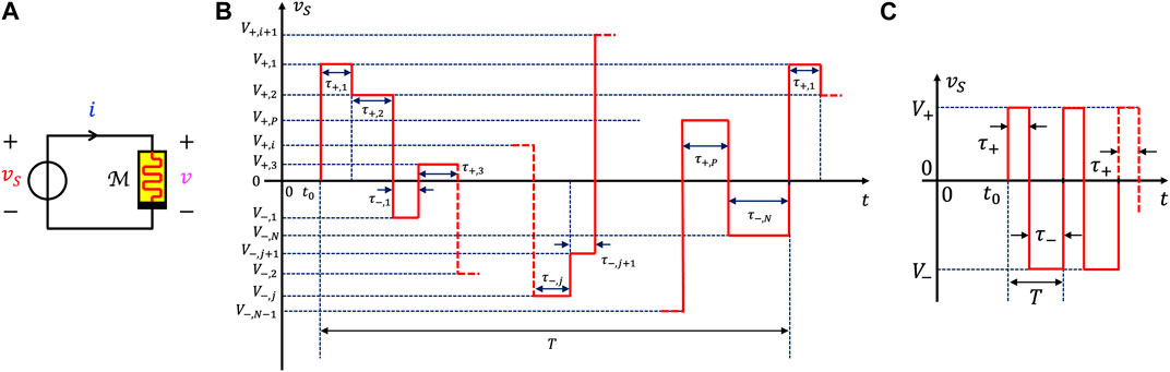
FIGURE 1. Circuit set-up (A) for the exploration of the response of the memristor
Consequently, any stimulus of this kind can be simply described by the associated parameter tuple (V+,1, τ+,1, … , V+,P, τ+,P, V−,1, τ−,1, … , V−,N, τ−,N). Crafting the pulse train with just two pulses per cycle, as in the study from Pershin and Slipko, the memory state of the ReRAM cell across which it is applied may be found to undergo one of at most two different locally stable limit-cycle oscillations after transients decay to zero (Pershin and Slipko, 2019a), depending upon its initial condition. On the other hand, increasing Q past 2, the periodically driven memristor may be endowed with a number of distinct oscillatory modes progressively larger than 2 at steady state, as revealed later on in section 4. Let us now briefly review the standard analysis tool proposed by Pershin and Slipko for investigating the nonlinear dynamics of periodically forced memristors.
3.1 The Time Average State Dynamic Route
By shaping the AC periodic voltage stimulus from Figure 1A in such a way that it would induce small changes in the memory state of the ReRAM cell (Messaris et al., 2023) across which it is applied over each cycle, precious insights into the response of the memristive device may be gained from the6 Time Average State Equation (TA-SE). Let us define the mean value of the memory state7 of the periodically driven ReRAM cell at any given time t ≥ t0, with t0 denoting the time instant at which the stimulus from Figure 1A is first applied between the device terminals, as
Employing the Leibniz integral formula, and making use of Equations 1–3, the derivative of the time average state with respect to the time may be expressed via
where τk ∈ {τ+,1, τ+,2, … , τ+,P, τ−,1, τ−,2, … , τ−,N}, Vk ∈ {V+,1, V+,2, … , V+,P, V−,1, V−,2, … , V−,N}, and tk = tk−1 + τk. Now, invoking the aforementioned hypothesis on the input shape, it is assumed that replacing the memory state by its time average in each of the Q integrands from Equation 9 does not introduce a noticeable error in the resulting approximation (Messaris et al., 2023). The TA-SE is then cast in the form (Pershin and Slipko, 2019a)
where the explicit dependence of the left hand side upon the time has been omitted, while.
May be respectively referred to as SET and RESET TA-SE components, given the sign invariance of the state evolution function 1) in the memristor model under focus. For Q = 2, with P = N = 1 (refer to Figure 1C), the formulas for the SET and RESET TA-SE components reduce to.
where (V+, τ+) and (V−, τ−) are the positive SET and negative RESET pulse height-width pairs, respectively (Pershin and Slipko, 2019a). Importantly, a TA-SE is strictly associated to a given stimulus as well as to a specific model. The formulation in Equation 10 provides an approximation for the ODE, which governs the time evolution of the time average state of the ReRAM cell under a particular periodic input belonging to the class illustrated in Figure 1B, and on the basis of the Strachan model (Strachan et al., 2013). As sketched qualitatively through an exemplary blue (red) trace in Figure 2A, plotting the right hand side of Equation 11 ((12)) versus the time average state, which is constrained to assume values in the closed set
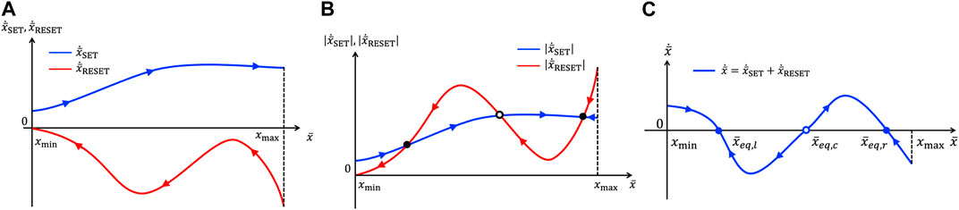
FIGURE 2. Visualization of exemplary graphs, enabling studying the response of the time average state of the ReRAM cell to the application of a specific AC periodic voltage stimulus belonging to the class illustrated in Figure 1B between its terminals, as shown in plot (a) of the same figure. Here, xmin =0 and xmax =1, in agreement with the Strachan memristor model. (A) Loci of the SET
3.2 The State Change Per Cycle Map: a novel system-theoretic tool for exploring the response of a ReRAM cell to any AC periodic stimulus
The novel graphic tool to be introduced and discussed shortly is inspired by the Poincaré Map Technique (Ascoli et al., 2005), a powerful analysis method from the theory of nonlinear dynamics. Let us then provide a pedagogical introduction to this precious investigation method, first introduced by the French mathematician Jules Henri Poincaré (1854–1912).
B.1 The Poincaré Map.The Poincaré Map Technique enables one to study the nonlinear dynamics of an nth-order continuous-time system through the investigation of a simpler (n − 1)-dimensional discrete-time one. This analysis tool requires a preliminary choice for an (n − 1)-dimensional sub-space, called Poincaré section, here indicated as Π.
Let us first assume the nth-order continuous-time system to be autonomous8. Its state vector is denoted here as
Focusing now on the class of case studies our periodically driven ReRAM cell falls into, let us consider an nth-order non-autonomous10 continuous-time system with state vector
Studying a Poincaré map allows one to gain precious insights on the nonlinear dynamics of the original continuous-time system, whether the latter be autonomous or non-autonomous. Our ReRAM cell is a first-order system. The Poincaré map of a first-order system under periodic stimulation reduces to the one-dimensional form

FIGURE 3. (A) Magenta curve: exemplary illustration of a Poincaré map
Remark 1. Given a one-dimensional Poincaré map
1. Find the point on the graph of the map of interest with abscissa x0. The ordinate of this point is
2. Draw an horizontal line from this point to the graph of the identity map. The horizontal and diagonal lines meet at the point (x (1), x (1)).
3. A vertical line drawn through this point is found to intersect the graph of the map of interest at a location with coordinates (x (1), x (2)), where
Given a generic map
B.2 The State Change Per Cycle Map.In some cases, especially for stimulus parameter settings whereby the memory state undergoes negligible changes over each input cycle across its entire existence domain
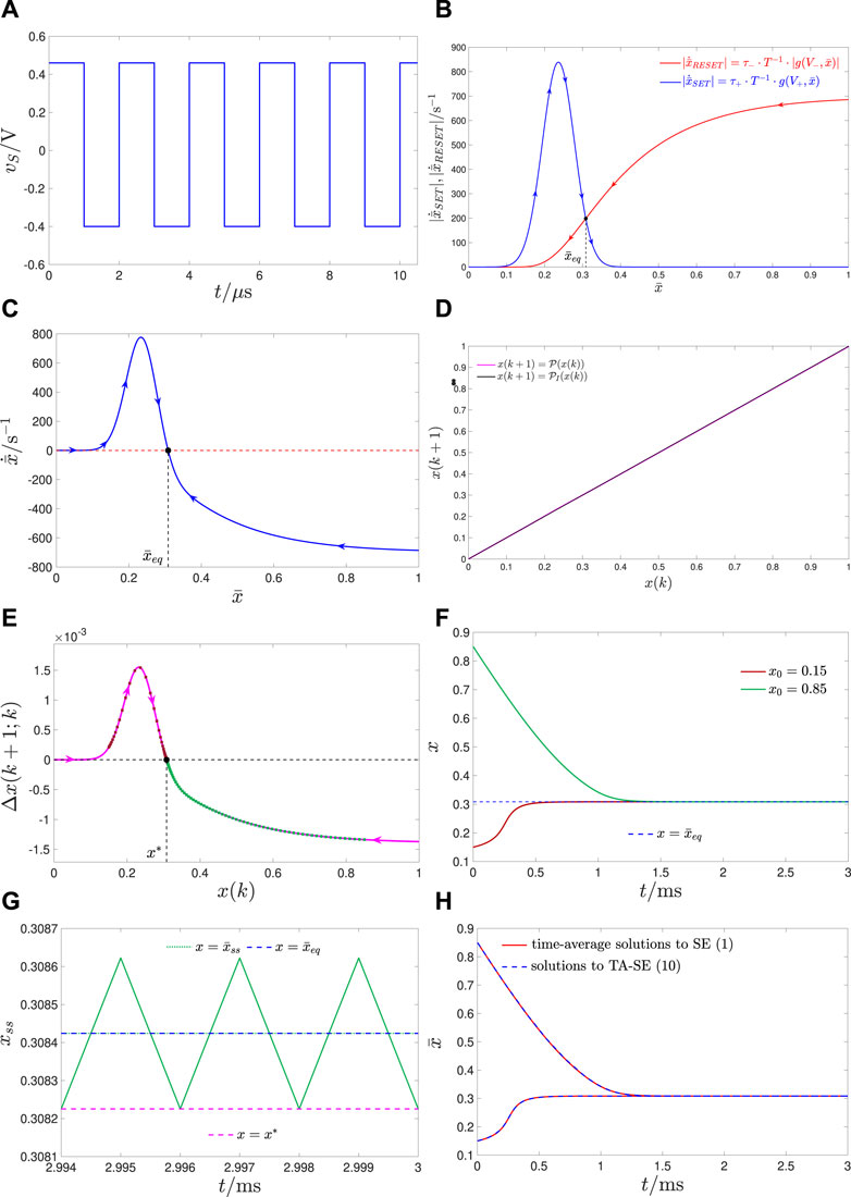
FIGURE 4. Case study 4.1.1 on the input-induced ReRAM cell mono-stability: (A) Voltage waveform generated by the AC periodic source vS across the memristor (see Figure 1A). With reference to the stimulus parameters defined in Figure 1C, the first SET and second RESET rectangular pulses in the input pulse doublet within each cycle feature height-width pairs (V+, τ+)=(0.46V,1 µs) and (V−, τ−)=(−0.4V,1 µs), respectively. Here, the input period T is equal to 2μs and t = t0=0s. (B) Blue (Red) trace: graph of the SET (RESET) TA-SE component versus the time average state. As indicated by the arrows on the first (latter) trace, the SET (RESET) dynamics, active as the positive (negative) pulse stimulates the device, determine a progressive increase (decrease) in the time average state. The TA-SE (10), tailored to this input, features a single equilibrium at
With reference to Figure 3, the magenta trace in plot b) qualitatively depicts the locus of Δx (k + 1; k) versus x(k), which corresponds to the Poincaré map from plot a). The magenta trace shows the graph of an exemplary SCPCM, characterizing the oscillatory response of the ReRAM cell to the periodic stimulation envisaged in the pedagogical case study from Figure 2. The same information, extracted from the Poincaré map, may be retrieved from the associated SCPCM. For example, the sequence of return points x (1), x (2), …, associated with a given initial condition x (0), may be easily inferred from Equation 15, given that x (k + 1) = x(k) + Δx (k + 1; k),
Remark 2. A time-efficient approach to derive the graph of the SCPCM of the ReRAM cell under the application of any given AC periodic stimulus between its terminals, either experimentally, in the case where the device memory state is physically accessible, or numerically, where a predictive model for the nonlinear dynamics of the non-volatile memristor is available, envisages the following steps. Preliminarily, a set of regularly spaced values
4 Application of the theory
This section, composed of two sub-sections, shall provide strong evidence for the significance of the novel analysis tool for the investigation of the response of an arbitrary first-order ReRAM cell to AC periodic stimuli of any kind. In the first subsection 4.1, the properties of the pulse train stimulus, applied across the particular memristor under focus in this manuscript, are carefully set (Messaris et al., 2023) so as to guarantee a small change in the respective memory state per cycle, which is the conditio sine qua non, to endow the TA-SDR investigation tool with a good predictive capability. In the second subsection 4.2, scenarios where either the pulse train stimulus or a triangular wave induces non-negligible changes in the device memory state per cycle shall be investigated, revealing the general applicability of the proposed system-theoretic technique to explore the nonlinear dynamics of the periodically driven ReRAM cell.
4.1 From mono-stability to multi-stability
In the three case studies13 discussed in this sub-section, the pulse train stimulus shall be respectively crafted in such a way to induce mono-stability, bi-stability, and tri-stability in the oscillatory dynamics of the non-volatile memristor from HP Labs (refer to Figure 4; Figure 5; Figure 6, respectively).
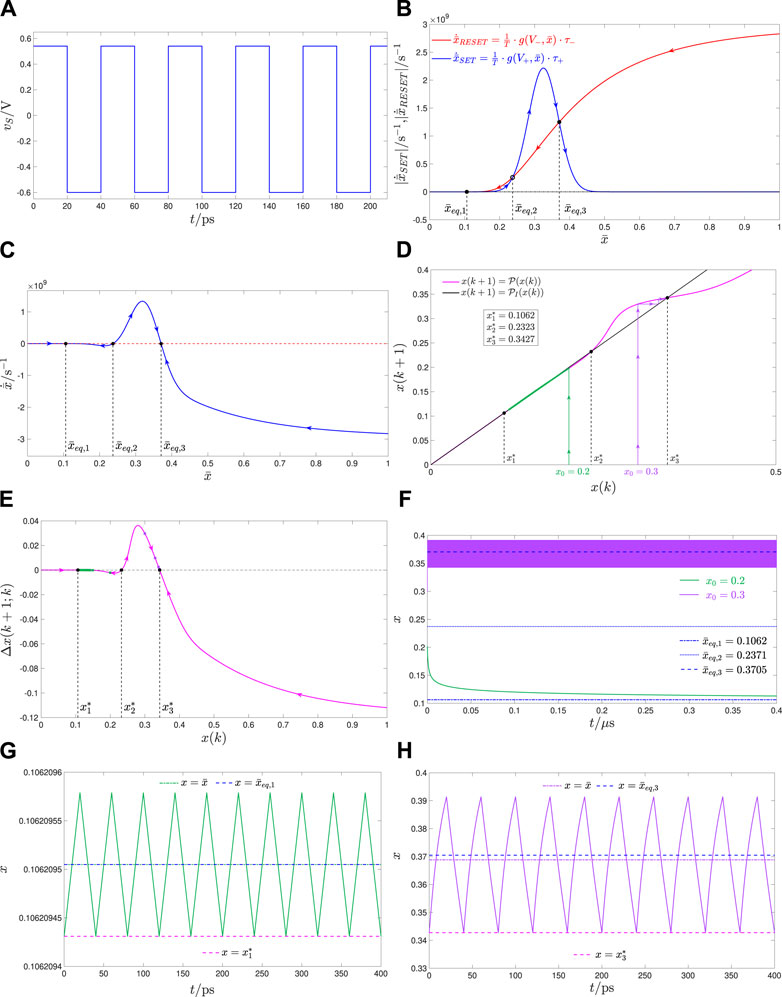
FIGURE 5. Case study 4.1.2 on the input-induced ReRAM cell bi-stability: (A) Rectangular pulse train-based voltage stimulus vS for the ReRAM cell in the test circuit of Figure 1A. With reference to plot (c) in the same figure, the tuple defining the input signal is here (V+, τ+, V−, τ−)=(+0.54 V,20 ps,−0.6 V,20 ps). The input period is then T = τ++ τ−=40 ps. Here, t = t0=0s. (B) Blue (red) trace: locus of
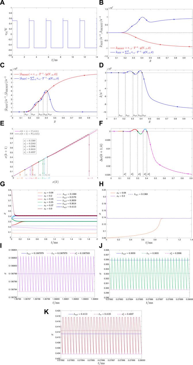
FIGURE 6. Case study 4.1.3 on the input-induced ReRAM cell tri-stability: (A) Time waveform of a pulse train-based voltage signal, which, stimulating the ReRAM cell, as illustrated in the circuit of Figure 1A, induces the emergence of a more interesting form of local fading memory, namely, tri-stability, across its physical stack. The input belongs to the class of Figure 1B, being composed of Q =3 consecutive pulses per cycle. The first, second, and third pulse in each cycle of the pulse train feature heights V+,1=0.6V, V+,2=0.51V, and V−,1=−0.52V, and widths τ+,1=3⋅10−19s, τ+,2=0.8⋅10−9s, and τ−,1=2⋅10−9s, respectively. Thus, here, p =2 and N =1. Moreover, the input period amounts to T = τ+,1+ τ+,2+ τ+,3=2.8 ns, while t0=0s. (B) Blue (Red) trace: graph of the SET (RESET) TA-SE component
Remark 3. Remarkably, as shown in the last figure, a more elaborate variant of the pulse train adopted in the study from Pershin and Slipko in (Pershin and Slipko, 2019a) allows one to endow the ReRAM cell with tri-stability. A systematic method enabling one to induce the emergence of a predefined number of oscillatory dynamical phenomena in the nano-device under pulse train stimulation, including an interesting discussion on potential applications, is about to appear shortly in (Ascoli et al., 2023).
4.2 On the general applicability of the SCPCM analysis tool
In the examples to follow, the stimulus applied across the ReRAM cell induces major changes in its memory state over each cycle. In these circumstances, the time averaging-based approximation of the Strachan model loses reliability, and, consequently, the predictions of the standard TA-SDR analysis tool are either prone to error (refer to the case study illustrated in Figure 7) or completely wrong (see the case studies in Figure 8; Figure 9). On the other hand, as revealed in Figures 7–9, the SCPCM investigation tool enables accurate estimation of both the number and the stability properties of the possible oscillatory modes for the periodically driven non-volatile memristor, irrespective of the input characteristics. Last but not least, and very importantly, the SCPCM tool is also applicable in scenarios where the ReRAM cell is stimulated via AC periodic stimuli other than the pulse trains considered so far, as demonstrated in the final case study illustrated in Figure 10, which provides further evidence for the superior performance of the novel system-theoretic technique over the standard TA-SDR method.
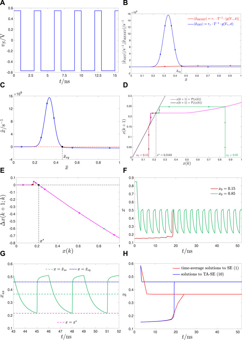
FIGURE 7. Case study 4.2.1 on the SCPCM accuracy in predicting the asymptotic memristor response upon large state excursions per input cycle: (A) Time course of the voltage signal vS, acting as an AC periodic stimulus for the ReRAM cell in the circuit of Figure 1A. The first SET and second RESET pulses, which, as sketched in plot (c) from the same figure, compose the excitation waveform in each cycle, of duration T = τ++ τ−=3ns, have height-width pairs (V+, τ+)=(0.55V,1ns) and (V−, τ−)=(−0.57V,2ns), respectively. Here, t0=0s. (B) Blue (Red) trace: locus of

FIGURE 8. Case study 4.2.2 on the SCPCM accuracy in predicting the number (here, 1) of admissible and stable memristor oscillatory modes upon large state excursions per input cycle: (A) Time waveform of the AC periodic voltage signal applied across the ReRAM cell in the test circuit of Figure 1A. With reference to plot (C) from the same figure, vS is unequivocally identified through the tuple (V+, τ+, V−, τ−)=(0.52 V,15⋅10−3s,−0.58 V,2⋅10−3s). The input period is T = τ++ τ−=17⋅10−3s. Once again, t0=0s. (B) Blue trace: TA-SDR associated with the pulse train-based stimulus from plot (A). The TA-SE (10) admits here three equilibria, of which the outer ones, specifically
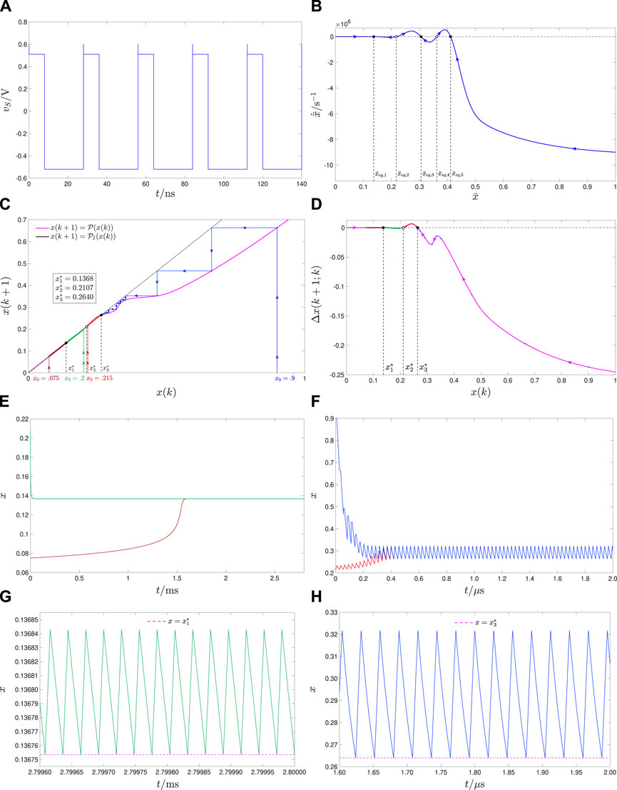
FIGURE 9. Case study 4.2.3 on the SCPCM accuracy in predicting the number (here, 2) of admissible and stable memristor oscillatory modes upon large state excursions per input cycle: (A) Time evolution of the pulse train-based voltage signal, which stimulates the ReRAM cell in the circuit from Figure 1A. With reference to plot (B) from the same figure, three are the pulses, which the train accommodates over each cycle, i.e., Q =3 here. The height-width pairs of the pulses are (V+,1, τ+,1)=(0.6 V,3⋅10–18 s) (V+,2, τ+,2)=(0.51 V,8⋅10–9 s), and (V−,1, τ−,1)=(−0.52 V,20⋅10–9 s) (thus p =2, and N =1). The input period is then T = τ+,1+ τ+,2+ τ−,1=28⋅10−9s, whereas t0=0s. (B) Blue trace: TA-SDR of the memristive system in the periodic stimulation scenario illustrated in plot (A). In this example, five are the equilibria of the TA-SE (10), namely,
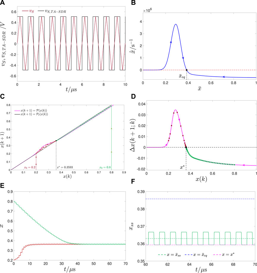
FIGURE 10. Case study 4.2.4 on the input-agnostic SCPCM predictive capability: (A) Magenta trace: AC periodic triangular voltage waveform vS, featuring amplitude V =0.5V, offset V0=0.01V, and period T =1⋅10−6s, and let fall across the ReRAM cell from t0=0s in the test circuit from Figure 1A. Black trace: Pulse train-based voltage signal vS,TA−SDR, employed as an approximation of the triangular wave stimulus, so as to enable the application of the TA-SDR analysis tool in this case study. The pulse train falls into the class depicted in Figure 1C, accommodating two pulses per cycle, specifically first a SET one of height V+=0.51 V and width τ+=5.1⋅10−7s, and then a RESET one of height V−=−0.49 V and width τ−=4.9⋅10−7s. (B) Blue trace: TA-SDR of the ReRAM cell under the assumption that the pulse train-based voltage waveform vS,TA−SDR from plot (A) falls between its terminals. The TA-SE (10) admits one globally asymptotically stable equilibrium at
4.3 Discussion
Comparing the TA-SDR and SCPCM analysis methods, the technique from Pershin and Slipko, revolving around a time averaging approximation of the device model, is trustworthy only in excitation scenarios where approximating the memory state of the periodically forced ReRAM cell with its time average in each input cycle is reasonable, whereas the tool proposed in this manuscript, relying strictly on the true un-approximated switching kinetics of the memory state, enables one to accurately explore the response of a first-order memristor to any kind of AC periodic stimulation. Provided physical measurements of the memory state of a device were feasible, the SCPCM tool more naturally lends itself to experimental validation. In fact, acquiring a TA-SDR in the lab would be cumbersome as it would preliminarily require estimation of the time derivative of the state across its existence domain under the application, across the ReRAM cell of each DC voltage from a set, including the heights of all the pulses and composing the input train over each cycle according to Equations 10 and 11, and 12. However, upon availability of a predictive device model, the derivation of a TA-SDR is computationally inexpensive, as it merely requires plotting the time average state evolution function versus the time average state, while the acquirement of a SCPCM envisages the run of a number of numerical simulations. A couple of important observations should be made at this point in regard to the examples from case studies 4.1.3 and 4.2.3. They call for the use of rather small input pulse widths. To the best of our knowledge, no instrumentation tool available nowadays would be capable of producing a pulse with a temporal width of the order of 10−19s in a practical experiment. As a result, future research efforts shall be devoted to the development of a strategy that allows increasing the minimum input pulse width without jeopardizing the device response of interest. Perhaps some adaptation of the simple experimental set-up shown in Figure 1A shall allow us to resolve the issue; however, its design might take a long time and is reserved for a future publication. It is important to remark, however, the theoretical relevance of these two examples, granted that the Strachan model is capable of predicting the nonlinear dynamics of the HP Ta2O5−x nano-device with high accuracy, as demonstrated in the seminal work (Ascoli et al., 2016c) in the past. In fact, as established by the TA-SE (10), each pulse contributes to the device time average kinetics as an additive term, appearing on the right hand side of the same equation and consisting of the product between the ratio between its time duration and the input period and the value of the time average state evolution function, evaluated at the voltage level and corresponding to the pulse amplitude, as shown in (11) and 12 for the SET and RESET cases, respectively. Therefore, even if a pulse has a rather short temporal width, it may still have a significant impact on the device time average dynamics because this is also affected by the range of values assumed by the time average state evolution function for the DC level corresponding to the pulse amplitude across the domain of existence of the device state (for the Strachan model, such a range can span several orders of magnitudes and its upper bound may be as high as 1035s−1 for a voltage level of just 0.7V, as shown in Fig. 15a) from (Demirkol et al., 2022)). On the basis of these observations, were it possible 1 day in the near future to avail of instrumentation tools capable to generate pulses of temporal widths on the order of 10−19s, the theoretically sound predictions from examples 4.1.3 and 4.2.3 could be experimentally tested. Furthermore, it is fair and worthy to mention that the unique opportunity offered by the analysis technique from Pershin and Slipko to decompose the time average state evolution function into SET and RESET components, allows the development of a system-theoretic procedure, enabling the setting of number, heights, and widths of the pulses within each period of a train stimulus so as to endow the ReRAM cell with as many locally stable steady-state oscillatory modes as desired, as discussed in (Ascoli et al., 2023). Here, the SCPCM tool can be used for verification purposes, so as to validate the theoretical predictions drawn from the TA-SDR analysis. Finally, with an outlook on other research works planned in our agenda, the evaluation of the transient dynamics of a non-volatile memristor ((Slipko and Pershin, 2019; Slipko and Pershin, 2021)) toward the respective asymptotic behavior in response to a given stimulus is worthy of consideration, especially in view of an in-depth evaluation of the practical feasibility of a potential exploitation of its peculiar features, including, in relation to the work presented in this manuscript, its global and local fading memory properties.
5 Conclusion
While the response of a first-order ReRAM cell may be completely characterized by means of a standard Dynamic Route Map analysis (Ascoli et al., 2022a), no homologous tool has ever been introduced for exploring the nonlinear dynamics of a memristive nanodevice of this kind under any AC excitation. In order to fill this gap in the literature, Pershin and Slipko (Pershin and Slipko, 2019a) recently proposed a new insightful method, which revolves around a time averaging-based approximation of the mathematical description of a first-order memristive device, and is applicable in scenarios where the memristive device itself is driven by pulse train-based stimuli (refer to (Pershin and Slipko, 2019b) for more insights). As shown in (Pershin and Slipko, 2019a), when applied to the predictive model (Strachan et al., 2013) of a first-order ReRAM cell from Hewlett Packard (HP) Labs, this method, which we call Time Average State Dynamic Route, enables one to infer the time evolution of the mean value of the device memory state under the assumption that the pulse train-based voltage stimulus, falling across the non-volatile memristor, induces small changes in the memory state itself over each cycle. In order for such an assumption to hold true, the amplitudes of the pulses included over each cycle in the waveform of the AC periodic stimulus, as well as the input frequency, must be carefully chosen, as thoroughly explained in (Messaris et al., 2023). A ReRAM cell is typically excited by pulse trains; therefore, the Time Average State Dynamic Route enables us to investigate its behavior for a very important class of case studies. However, this tool is not rigorously applicable to studying the device response to other AC periodic excitations. Motivated by the necessity to derive a more general analysis method for periodically driven ReRAM cells, this manuscript introduces a novel system-theoretic tool, referred to as State Change Per Cycle Map, which is inspired by the Poincaré Map technique, and is applicable in all case studies where an arbitrarily shaped AC periodic signal stimulates a first-order device of this kind. The new tool enables one to infer the change that the device memory state undergoes during one complete cycle of the stimulus from any of its admissible values. In particular, it allows us to determine the number and stability properties of all the possible oscillatory modes of the periodically driven nano-device, which is effectively a second-order autonomous continuous-time system, through the investigation of a simpler one-dimensional discrete-time one (Ascoli et al., 2005). Light is shed on the significance and general applicability of the proposed system-theoretic tool through the analysis of a number of illustrative case studies. The State Change Per Cycle Map technique could be employed to explore a time- and energy-efficient approach to program a ReRAM cell. An in-depth study of this kind could allow the synthesis of a look-up table, which would provide the most appropriate characteristics of a suitable AC periodic stimulus for programming a ReRAM cell from a given initial state into a desired final one within the shortest time and at the lowest possible energy cost. Last but not least, the manuscript reveals, for the first time, how applying, across the ReRAM cell, a pulse train more elaborate than the stimulus employed in the study from Pershin and Slipko may induce the asymptotic convergence of the respective memory state toward any of a number of locally stable oscillatory waveforms larger than two, depending upon the initial condition (see (Ascoli et al., 2023) for more details). This research study contributes to laying the foundations of memristor theory, providing the research community with a new, powerful analysis tool to unlock the full potential of memristive nanotechnologies for the electronics of the future.
Data availability statement
The raw data supporting the conclusions of this article will be made available by the authors, without undue reservation.
Author contributions
AA and NS conceived the theoretical framework, and wrote the manuscript. AA, NS, IM, and ASD performed the numerical simulations to validate the theory. RT, and LC supported the research work, providing precious suggestions, and constructive comments. All authors contributed to the article and approved the submitted version.
Funding
LC is supported in part by USA Air Force Office of Scientific Research (AFOSR) grant number FA 9550-18-1-0016.
Acknowledgments
The authors wish to thank the Editor and the Reviewers for the highly-professional constructive criticism, which helped us to improve considerably the manuscript relative to its original version.
Conflict of interest
The authors declare that the research was conducted in the absence of any commercial or financial relationships that could be construed as a potential conflict of interest.
Publisher’s note
All claims expressed in this article are solely those of the authors and do not necessarily represent those of their affiliated organizations, or those of the publisher, the editors and the reviewers. Any product that may be evaluated in this article, or claim that may be made by its manufacturer, is not guaranteed or endorsed by the publisher.
Footnotes
1Referring, without loss of generality, to a voltage-controlled first-order memristor, with Differential Algebraic Equation (DAE) set (1)–(2), its DRM is a family of State Dynamic Routes (SDRs), each of which visualizes the time derivative
2The interested reader is invited to consult (Messaris et al., 2023) for more details on the constraints to be enforced on the ReRAM stimulus for the application of the time averaging method to its mathematical description to deliver reliable predictions for the time evolution of the mean value of the respective memory state from a given initial condition.
3If v = 0, the memory state x of an analogue non-volatile memristor such as the one under consideration in this study, is motionless.
4The state evolution function g(x, v) in Eq. 1 is said to be sign-invariant (Chua, 2018), since it features the same sign as the voltage, falling across the memristor, irrespective of the state variable value.
5A system is said to have Fading Memory on a given input if it exhibits a unique asymptotic behavior, irrespective of the initial condition, as it is exposed to its stimulation. In case, on the other hand, a forced system may feature one of a set of distinct operating modes, at the end of the transient phase, depending upon the initial state, it is said to have Local Fading Memory on the respective stimulus. Input-induced fading memory effects were first discovered in a ReRAM cell from HP Labs back in 2016. As revealed more recently (Ascoli et al., 2023), under suitable stimulation the very same non-volatile memristor may experience local fading memory, endowing the ReRAM cell with an interesting multi-modal operating capability, which may be leveraged for application purposes.
6The TA-SE is an ODE, which predicts rather well the dynamical evolution of the time average of the state of a first-order memristor under pulse train stimulation, provided the input is shaped in such a way so as to trigger a rather slow device response over each period. Despite the fact that Pershin and Slipko did not coin a name for this ODE, they should be credited for its introduction in the bifurcation analysis of the Strachan DAE set (Strachan et al., 2013) reported in (Pershin and Slipko, 2019a). The TA-SE was recently employed in (Messaris et al., 2023) to study the response of the non-volatile memristor from HP Labs to high-frequency AC periodic excitations.
7For simplicity, the mean value of the memory state is referred to as time average state in the remainder of the paper.
8A nth-order continuous-time system is said to be autonomous if no input signal drives its dynamics, which are then only controlled by means of the initial conditions assigned to its n state variables.
9The sequence of time instants
10An nth-order continuous-time system is said to be non-autonomous if some input signal controls its dynamics.
11An nth-order non-autonomous ODE of the form
12With f′(⋅) denoting the derivative of a function
13Without loss of generality, in each of the AC periodic stimuli shown in Figures 4A, 5A, 6A, the sequence of pulses included in the train over each cycle is arranged in such a way to accommodate only one RESET pulse featuring a negative height at its very end. As a result, inspecting the behavior of the device, evolving from a certain initial condition in response to any of these excitation signals, the sample of the memory state at the end of each input period, after transients decay to zero, coincides with the minimum of the asymptotic oscillatory solution to the periodically driven continuous-time ODE 1), adapted to the Strachan state evolution function, expressed by Eqs 3, 4, and 5. In each of these ReRAM cell excitation scenarios, a stable (an unstable) fixed point x* for the relevant one-dimensional discrete-time system
References
Ascoli, A., Demirkol, A. S., Tetzlaff, R., and Chua, L. O. (2022b). Edge of chaos is sine qua non for turing instability. IEEE Trans. Circuits Systems-I (TCAS-I) Regul. Pap. 69 (11), 4596–4609. doi:10.1109/tcsi.2022.3194465
Ascoli, A., Demirkol, A. S., Tetzlaff, R., and Chua, L. O. (2022c). Edge of chaos theory resolves smale paradox. IEEE Trans. Circuits Systems-I (TCAS-I) Regul. Pap. 69 (3), 1252–1265. doi:10.1109/tcsi.2021.3133627
Ascoli, A., Demirkol, A. S., Tetzlaff, R., Slesazeck, S., Mikolajick, T., and Chua, L. O. (2021a). On local activity and edge of chaos in a NaMLab memristor. Front. Neurosci. 15 (651452), 651452. doi:10.3389/fnins.2021.651452
Ascoli, A., Mahon, A., and Feely, O. (2005). Nonlinear dynamics of first- and second-order log-domain circuits. IEEE Trans. Circuits Systems-I (TCAS-I) Regul. Pap. 52 (7), 1372–1381. doi:10.1109/tcsi.2005.851715
Ascoli, A., Menzel, S., Rana, V., Kempen, T., Messaris, I., Demirkol, A. S., et al. (2022a). A deep study of resistance switching phenomena in TaOx ReRAM cells: system-theoretic dynamic Route map analysis and experimental verification. Adv. Electron. Mater., 8 (8), 2200182. doi:10.1002/aelm.202200182
Ascoli, A., Schmitt, N., Messaris, I., Demirkol, A. S., Tetzlaff, R., Strachan, J. P., et al. (2023). “Multistability in the response of a ReRAM cell from Hewlett packard labs to pulse train stimulation,” in IEEE trans. On circuits and systems–I: Regular papers (TCAS-I) (IEEE), in preparation.
Ascoli, A., Tetzlaff, R., Chua, L. O., Strachan, J. P., and Williams, R. S. (2016c). History erase effect in a non-volatile memristor. IEEE Trans. Circuits Systems–I (TCAS–I) Regul. Pap. 63 (3), 389–400. doi:10.1109/tcsi.2016.2525043
Ascoli, A., Tetzlaff, R., and Chua, L. O. (2016a). The first ever real bistable memristors–Part I: theoretical insights on local fading memory. IEEE Trans. Circuits Systems–II Express Briefs 63 (12), 1091–1095. doi:10.1109/tcsii.2016.2604567
Ascoli, A., Tetzlaff, R., and Chua, L. O. (2016b). The first ever real bistable memristors–Part II: design and analysis of a local fading memory system. IEEE Trans. Circuits Systems–II Express Briefs 63 (12), 1096–1100. doi:10.1109/tcsii.2016.2613560
Ascoli, A., Tetzlaff, R., Kang, S. M., and Chua, L. O. (2021b). System-theoretic methods for designing bio-inspired mem-computing memristor cellular nonlinear networks. Front. Nanotechnol. 3 (633026), 33. doi:10.3389/fnano.2021.633026
Ascoli, A., Tetzlaff, R., and Menzel, S. (2018). Exploring the dynamics of real-world memristors on the basis of circuit theoretic model predictions. IEEE Circuits Syst. Mag. 18 (2), 48–76. doi:10.1109/mcas.2018.2821760
Boyd, S., and Chua, L. O. (1985). Fading memory and the problem of approximating nonlinear operators with Volterra series. IEEE Trans. Circuits Syst. 32 (11), 1150–1161. doi:10.1109/tcs.1985.1085649
Chua, L. O. (2018). Five non-volatile memristor enigmas solved. Appl. Phys. A 124 (563), 563. doi:10.1007/s00339-018-1971-0
Demirkol, A. S., Ascoli, A., Messaris, I., Al Chawa, M. M., Chua, L. O., and Tetzlaff, R. (2022). A compact and continuous reformulation of the strachan TaOx memristor model with improved numerical stability. IEEE Trans. Circuits Systems-I Regul. Pap. 69 (3), 1266–1277. doi:10.1109/tcsi.2021.3132278
Ielmini, D., and Waser, R. (2016). Resistive switching: From fundamentals of nanoionic redox processes to memristive device applications. first edition. Weinheim, Germany: Wiley VCH.
Messaris, I., Ascoli, A., Demirkol, A. S., and Tetzlaff, R. (2023). High frequency response of non-volatile memristors. IEEE Trans. Circuits Systems-I (TCAS-I) Regul. Pap. 70 (2), 566–578. doi:10.1109/tcsi.2022.3219368
Pershin, Y. V., and Slipko, V. A. (2019a). Bifurcation analysis of a TaO memristor model. J. Phys. D Appl. Phys. 52 (50), 505304. doi:10.1088/1361-6463/ab4537
Pershin, Y. V., and Slipko, V. A. (2019b). Dynamical attractors of memristors and their networks. Europhys. Lett. (EPL) 125 (2), 20002. doi:10.1209/0295-5075/125/20002
Pickett, M. D., and Williams, R. S. (2013). Phase transitions enable computational universality in neuristor-based cellular automata. Nanotechnology 24 (38), 384002. doi:10.1088/0957-4484/24/38/384002
Slipko, V. A., and Pershin, Y. V. (2021). Importance of the window function choice for the predictive modelling of memristors. Trans. Circuits Syst. II Express Briefs 68 (6), 2167–2171. doi:10.1109/tcsii.2019.2906295
Slipko, V. A., and Pershin, Y. V. (2019). Transient dynamics of pulse-driven memristors in the presence of a stable fixed point. Phys. E Low-dimensional Syst. Nanostructures 114 (113561), 113561. doi:10.1016/j.physe.2019.113561
Strachan, J. P., Torrezan, A. C., Miao, F., Pickett, M. D., Yang, J. J., Yi, W., et al. (2013). State dynamics and modeling of Tantalum oxide memristors. IEEE Trans. Electron Devices 60 (7), 2194–2202. doi:10.1109/ted.2013.2264476
Strogatz, S. H. (2015). Nonlinear dynamics and chaos: With applications to physics, biology, chemistry, and engineering. second edition. Boulder, Colorado, United States: Westview Press.
Yang, J. J., Zhang, M. X., Strachan, J. P., Miao, F., Pickett, M. D., Kelley, R. D., et al. (2010). High switching endurance in TaOx memristive devices. Appl. Phys. Lett. 97 (23), 232102. doi:10.1063/1.3524521
Keywords: ReRAM, non-volatility, fading memory, local fading memory, multi-stability, State Change Per Cycle Map, Poincaré Map
Citation: Ascoli A, Schmitt N, Messaris I, Demirkol AS, Tetzlaff R and Chua LO (2023) The State Change Per Cycle Map: a novel system-theoretic analysis tool for periodically-driven ReRAM cells. Front. Electron. Mater. 3:1228899. doi: 10.3389/femat.2023.1228899
Received: 25 May 2023; Accepted: 16 August 2023;
Published: 12 September 2023.
Edited by:
Yuriy Pershin, University of South Carolina, United StatesReviewed by:
Clodoaldo Irineu Levartoski de Araujo, Universidade Federal de Viçosa, BrazilValeriy Slipko, Opole University, Poland
Copyright © 2023 Ascoli, Schmitt, Messaris, Demirkol, Tetzlaff and Chua. This is an open-access article distributed under the terms of the Creative Commons Attribution License (CC BY). The use, distribution or reproduction in other forums is permitted, provided the original author(s) and the copyright owner(s) are credited and that the original publication in this journal is cited, in accordance with accepted academic practice. No use, distribution or reproduction is permitted which does not comply with these terms.
*Correspondence: A. Ascoli, YWxvbi5hc2NvbGlAdHUtZHJlc2Rlbi5kZQ==