 Keshari Nandan
 Amit Agarwal
 Somnath Bhowmick
 Yogesh S. Chauhan
- 1Department of Electrical Engineering, IIT Kanpur, Kanpur, India
- 2Department of Physics, IIT Kanpur, Kanpur, India
- 3Department of Material Sciences and Engineering, IIT Kanpur, Kanpur, India
Two-dimensional (2-D) semiconductors are emerging as strong contenders for the future of Angstrom technology nodes. Their potential lies in enhanced device scaling and energy-efficient switching compared to traditional bulk semiconductors like Si, Ge, and III-V compounds. These materials offer significant advantages, particularly in ultra-thin devices with atomic scale thicknesses. Their unique structures enable the creation of one-dimensional nanoribbons and vertical and lateral heterostructures. This versatility in design, coupled with their distinctive properties, paves the way for efficient energy switching in electronic devices. Moreover, 2-D semiconductors offer opportunities for integrating metallic nanoribbons, carbon nanotubes (CNT), and graphene with their 2-D channel materials. This integration helps overcome lithography limitations for gate patterning, allowing the realization of ultra-short gate dimensions. Considering these factors, the potential of 2-D semiconductors in electronics is vast. This concise review focuses on the latest advancements and engineering strategies in 2-D logic devices.
Introduction
In 2004, a groundbreaking discovery marked the beginning of a new era in materials science: isolating a single layer of graphite from its bulk form (Novoselov et al., 2004; Novoselov et al., 2005; Novoselov, 2011). This revolutionary achievement led to the emergence of an exciting family of 2-D materials. The remarkable graphene is at the forefront of this family, composed of just a single layer of graphite. Graphene’s extraordinary physical and electronic properties have captivated researchers worldwide, making it the most extensively studied 2-D material. Its unique characteristics hold the promise of unlocking a multitude of transformative applications across various fields. From revolutionizing electronics and optoelectronics to advancing biomedical and electrochemical technologies, graphene’s potential knows no bounds. This incredible material has opened doors to innovation and sparked a wave of scientific exploration, fueling hopes for a brighter and more technologically advanced future. It has the minimum possible thickness, is the strongest material (∼200 times stronger than steel), is an exceptional heat conductor, is almost transparent, lightweight, flexible, and the best electrical conductor at room temperature. The electrons in this material behave differently than other known materials, manifesting in several fundamental discoveries like Klein tunneling, the half-integer quantum Hall effect, and electrons as massless particles, to name a few. In 2010, the “Nobel Prize” was awarded to Andre Geim and Konstantin Novoselov for this remarkable discovery. A zero band gap in graphene makes it undesirable for logic applications. Different approaches have been used to introduce band gaps in graphene, but they increase the fabrication complexity and reduce the mobility to the level of strained Si (Obradovic et al., 2006; Han et al., 2007; Jiao et al., 2009).
Around 2010, another class of 2-D material was discovered beyond graphene, known as transition metal dichalcogenides (TMDCs) (Mak et al., 2010; Splendiani et al., 2010). Unlike semi-metallic graphene, they are semiconductors with moderate bandgaps, which open other application fields like logic devices. MoS2, a member of the TMDCs family, has a band gap ∼ 1.8 eV, which is satisfactory for logic switches to discriminate between two logic states sharply. Also, combining a low dielectric constant (ϵch) and the ability to grow atomic layers within channels (tch = # of layers × thickness of monolayer) results in a reduced characteristic length
The crystallinity, purity, large-area growth, and thickness controllability of the grown 2-D channel material are essential for manufacturable device technology. For 2-D channel material growth, these targets must be fulfilled for industrialization. For large-area production, different methods have been used; promising ones are chemical vapor deposition (CVD) (Li et al., 2017; Lin et al., 2017), metal-organic chemical vapor deposition (MOCVD) (Lee et al., 2020; Maxey et al., 2022), liquid-phase exfoliation Shen et al., 2015; Coleman et al., 2011), epitaxial growth (Dong et al., 2020; Dong et al., 2022), and molecular beam epitaxy (MBE) (Cheng et al., 2020), to name a few. CVD is a widely used method to grow high-quality 2D materials. It allows scalability and is suitable for large-area growth, making it essential for industrial applications, but it requires precise temperature and pressure control. MOCVD is a variation of CVD that uses metal-organic precursors to grow 2-D materials. It offers reasonable control over film thickness and uniformity. MBE is a precise technique where atoms or molecules are deposited on a substrate to create thin films layer by layer. While it allows excellent control over layer thickness and composition, it is generally more complex and expensive than CVD. Epitaxy involves growing a crystalline film on a single-crystal substrate, producing high-quality, uniform 2-D layers.
Over the last decade, tremendous progress has been made in logic devices based on 2-D materials (see Figure 1). These include wafer-scale production of single-crystalline 2-D semiconductors and fabrication of logic devices at large scale, high-quality and ultralow-resistance metal contact to 2-D semiconducting channels, high-quality integration of 2-D channels with high-k oxides, demonstration of state-of-the-art devices on a wafer scale, breaking Boltzmann’s tyranny using the exotic and versatile E − k dispersion of 2-D materials, alleviation of the lithography limitations on gate patterning, and facilitation of ultra-short gate dimensions using CNTs, graphene, and metallic nanowires, to name a few. Several reports have been presented, discussing: i) the critical performance metrics for aggressively scaled 2-D transistors, offering their extraction and reporting guidelines (Das et al., 2021), materials preparation (Liu et al., 2017), electrical characterization Mitta et al. (2020), and ii) the promising potential of 2-D FETs in very large scale integration (VLSI) design (Fiori et al., 2014; Dorow et al., 2022; Knobloch et al., 2023; Naylor et al., 2023; Sheng et al., 2023). Here, we discuss the family of 2-D materials from the perspective of device design, recent developments to improve the performance of 2-D logic devices, and the unique features facilitated by 2-D semiconductors.
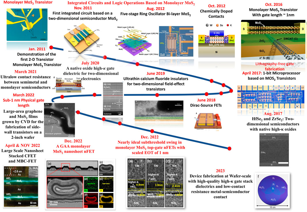
FIGURE 1. Major Milestones in the Development of 2-D Logic Devices: In 2011, a research breakthrough emerged from EPFL as they showcased the inaugural transistor utilizing monolayer MoS2. Following this milestone, subsequent years witnessed a series of demonstrations involving transistors crafted from transition metal dichalcogenides (TMDCs). The primary thrust was to enhance their performance while delving into integrated circuits built upon these materials. However, a notable stumbling block in this journey was achieving large-scale, single-crystalline growth and favorable interface properties with high-k oxides and metallic contacts. Over the past few years, commendable strides have been taken to overcome these hurdles, resulting in successful demonstrations that validate the progress made in tackling these significant issues.
Nanoelectronics-specific applications of the 2-D family
The versatile family of 2-D materials offers a broad spectrum of material properties, ranging from metallic and semi-metallic to semiconductor, insulator, topological insulator, ferroelectric, magnetic, and superconducting properties (Liu et al., 2016; Qi et al., 2021; Zhang et al., 2022a; Elahi et al., 2022). This extensive array of 2-D materials with customizable characteristics opens the door to atomic-scale heterogeneous integration. This, in turn, allows for the creation of innovative hybrid structures that showcase novel physical phenomena and provide unique functionalities (Geim and Grigorieva, 2013; Novoselov et al., 2016; Jie et al., 2018; Ghiasi et al., 2019). One can find a suitable material for integrated circuit applications within this diverse family. Figure 2 provides a glimpse of some nanoscale device applications employing materials from this class. In the following sections, we will explore the essential properties pertinent to front-end devices.
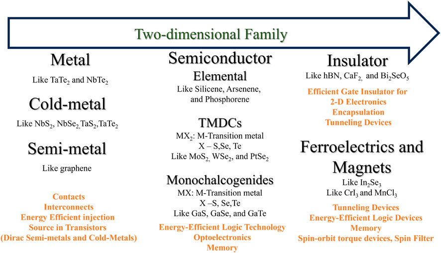
FIGURE 2. The 2-D material family encompasses a wide range of unique properties, each with its own set of applications when viewed through the lens of nanoscale devices.
Milestones in the development of 2-D materials based logic electronics
Metal contacts on 2-D semiconductors
Since doping foreign atoms into 2-D semiconductors is difficult and problematic because of the high probability of causing damage, source and drain electrodes’ work function is engineered to inject carries into a 2-D semiconductor channel. So, contact with these ultra-thin semiconductors is vital for harvesting their potential. During the initial years of development, reliable n-and p-type contacts have not been made to these ultra-thin semiconductors as direct metal deposition leads to interface defects and defects in the semiconductors. These undesirable effects pin the Fermi-level, and theoretically expected Schottky–Mott model (Mott, 1939; Schottky, 1939) results are not observed experimentally (Liu et al., 2018; Mleczko et al., 2019). For example, it is expected theoretically that Ag and Ti will work as n-type contact to MoTe2 and Ni, Au, and Pt will act as p-type contact. However, due to Fermi-level pinning (FLP) resulting from defects, the n-type contact is observed for all the metals with pinning factor (S) ∼ 0.06 (Mleczko et al., 2019). This value for S is almost close to pinned materials (S = 0). However, the ideal case is S = 1, which means ideal charge neutrality. Different strategies have been used to eliminate these defects and deepen the Fermi level. Prominent approaches include side metallic contact, use of hBN as a buffer layer over 2-D (Lizzit et al., 2022), ultraclean Ohmic vdW contacts (Boandoh et al., 2018; Wang et al., 2019; Kim et al., 2021; Jang et al., 2022; Wang and Chhowalla, 2022), different phases of 2-D material (Jiang et al., 2023), local doping, mechanical transfer of metal over 2-D (Liu et al., 2018), and semi-metallic contact (Chou et al., 2021; Shen et al., 2021; Jiang et al., 2023; Li et al., 2023; Wang et al., 2023), to name a few. The performance metrics of 2-D based FETs (fabricated devices) are plotted in Figure 3 for LG ≤ 50 nm. The best performance is achieved in InSe FET with semimetallic Y-InSe contact.
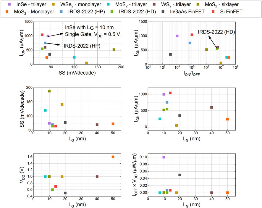
FIGURE 3. Comparision of performance metrics for 2-D based FETs with LG ≤ 50 nm (Natarajan et al., 2014; Yang et al., 2015; Nourbakhsh et al., 2016; Convertino et al., 2018; Zhu et al., 2018; Pang et al., 2020; O’Brien et al., 2021a; IRDS, 2021; Jiang et al., 2023). Metrics for IRDS expectation for 2037, Si FinFET, and InGaAs FinFET are also plotted for comparison.
Except for semi-metallic contact, other methods to decouple the metal-semiconductor interaction result in RC in the order of kΩ μm, which is one order higher than RC in Si-metal (Chhowalla et al., 2016). Also, local doping and mechanical transfer strategies are technologically challenging. However, the significant tunneling barrier in vdW contacts results in high RC, in the order of kΩ. Alternatively, semi-metallic contact with 2-D semiconductors suppresses metal-induced gap states (MIGS), resulting in gap state saturation (GSS) and Schottky barrier-free interface with ultralow RC, approaching the quantum limit. The devices with semi-metallic contact can potentially deliver performance for future
Insulator for 2-D electronics
Integrating channel material and scalable gate insulators with a high-quality interface, i.e., low defect density, is a stringent requirement in the semiconductor industry. Defects lead to undesirable effects in metal-oxide-semiconductor field-effect transistors (MOSFETs) and distort the characteristics, viz. charge trapping and de-trapping, bias temperature instabilities (BTI) (contributed by charge de-trapping), and mobility degradation (coulomb scattering due to trapped oxide charge), to name a few. Si technology is blessed due to the availability of a native oxide with a low defect density SiO2, also integrated with high-k insulators (like HfO2) with SiO2 as an interfacial layer using atomic layer deposition (ALD) (Green et al., 2001). However, this integration technique is not suitable in the case of 2-D materials due to its natural van der Waals (vdW) bonding in out-of-plane directions, which results in poor interfacial properties if one deposits oxides using ALD (Lemme et al., 2007). Surface treatments, like rapid thermal annealing (RTA), could reduce defects. Still, the defect density is high after surface treatments, which deteriorates the device’s performance. Another way is to use a molecular seeding layer of thickness ∼ 0.3 nm to grow HfO2 using ALD, resulting in uniform HfO2 with a minimum thickness of ∼ 1.5 nm (Li et al., 2019). The molecular seeding layer’s thickness is insufficient to block charge trapping due to oxide defects.
The widely known 2-D vdW insulator, hBN, has been used and shown ultra-clean interface with 2-D semiconductors. However, higher leakage and non-scalable process make the sub-1 nm EOT integration in 2-D electronics unsuitable (Britnell et al., 2012; Knobloch et al., 2021). Another crystalline insulator, CaF2, has been shown to have good interface quality and scalable down to 0.9 nm EOT (Illarionov et al., 2020). It is a good gate insulator for 2-D electronics. High-k native oxide, Bi2O2Se5, has been synthesized by layer-by-layer oxidation of Bi2O2Se, a high-mobility 2-D semiconductor with outstanding stability and excellent mechanical properties, and suitable for sub-0.5 nm EOT electronics (Li et al., 2020; Zhang et al., 2022b; Zhang et al., 2023). Recently, LaoBr, a rare earth oxyhalide, was synthesized with a static dielectric constant of
Sub-1 nm gate length: lithography-free process
Recent experimental reports demonstrate the feasibility of lithography-free ultra-short gate length in 2-D FETs, gated with core/shell nanowire with a minimum diameter of 6 nm (Cao et al., 2016), CNT with the physical gate length of
Breaking Boltzmann tyranny/energy-efficient switching: originating from intrinsic properties of 2-D materials
Overcoming Boltzmann’s tyranny is indeed a significant challenge in designing ultralow-power transistors. The concept refers to the fundamental limit imposed by thermal energy (kT) at room temperature, which sets a lower bound on traditional transistors’ subthreshold swing (SS). The subthreshold swing is related to the steepness of the current-voltage curve and directly impacts the transistors’ energy efficiency and power consumption. Two strategies have been explored to address this challenge: tunnel FETs (Appenzeller et al., 2004; Zhang et al., 2006; Nagavarapu et al., 2008) and Landau FETs (Salahuddin and Datta, 2008; Salvatore et al., 2008; Rusu et al., 2010). Tunnel FETs leverage quantum tunneling for carrier transport instead of traditional thermionic emission. By using a thin tunneling barrier, they can achieve steeper switching behavior, leading to lower SS and reduced power consumption. However, TFETs suffer from a limitation in the ON-state current due to the nature of tunneling transport. This restriction makes achieving sufficiently high current levels for practical applications challenging. Landau FETs rely on increasing the barrier height’s steepness with the application of gate voltages. This approach can potentially reduce the subthreshold swing and allow for ultralow-power operation. However, significant technological challenges are associated with Landau FETs, both at the material and device levels. One major issue is achieving low hysteresis while maintaining the required ON-state current (Lee et al., 2015; Li et al., 2015; Khan et al., 2016; Si et al., 2018). Hysteresis refers to the dependence of the transistor’s behavior on its history, and excessive hysteresis can negatively affect device performance and reliability.
The intrinsic exotic E-k dispersion in 2-D materials and their heterostructures offers alternative solutions to overcome Boltzmann’s tyranny in conventional FETs with 2-D materials as channel (Qiu et al., 2018; Liu et al., 2020a; Nadeem et al., 2021a; Liu et al., 2021; Tang et al., 2021). Below, the physical concepts of these devices are briefly described.
Dirac-source (DS)-FETs: Dirac materials, like graphene, as source in FETs
The carrier density decays sub-exponentially and exponentially with infinity thermal tail in conventional source FETs comprised of 3-D (like Si, Ge, III-V) and 2-D (like MoS2, MoSi2N4) semiconductors, respectively. Therefore, the SS is limited to ≥60 mV/decade at room temperature. However, the carrier density decays superexponentially in graphene and cuts down the infinite thermal tail, owing to linear dispersion E-k and Dirsc point in graphene. As a result, the FETs with graphene sources overcome Boltzmann’s tyranny and facilitate energy-efficient switching.
For the first time, in 2018, a group of researchers from China and Canada demonstrated the concept of DS-FETs by integrating graphene in a source of CNT-FET (Qiu et al., 2018). Unlike negative capacitance FETs, the reported device shows negligible hysteresis and meets the desired performance metrics for sub-60 mV/decade devices. The I60 lies in the range 1–40 μA/μm and SS
In principle, graphene/2-D semiconductors hetero-bilayers can show sub-60 mV/decade characteristics. Other reported system is graphene-MoS2 hetero-bilayer in conventional device structure (Liu et al., 2020b; Liu et al., 2021), state-of-the-art (GAA) device structure (Tang et al., 2021), and diode (Myeong et al., 2022). Graphene/MoS2 device shows I60 > 1 μA/μm with sub-60 SS over more than thee decades of drain current. In GAA structure, improved switching characteristics and 40% enhanced ON-state current. The diode based on graphene has shown a sub-unity ideality factor over more than four decades of change in current with a minimum ideality factor of 0.8 and rectification ratio
Topological FETs
The bandgap can be tuned in topological materials by applying a vertical electric field. Alternatively, the conduction is enabled by applying a vertical electric field due to quantum spin Hall effects resulting from Rashba spin-orbit interaction (Vergniory et al., 2019; Kumar et al., 2020; Gilbert, 2021). Recently, it has been shown that by using 2-D topological insulators as channels in conventional FETs, the incompressible limit on SS at room temperature can be overcome, and SS could be lowered by
All the above demonstrations are paving the path toward low-power electronic circuits.
Wafer-scale demonstration of 2-D fin field-effect transistors, multibridge-channel field-effect transistors (MBC-FETs) and complementary field-effect transistors (C-FETs)
The current mainstream device architecture, FinFETs, has taken us far in terms of CMOS scaling, but as we venture into sub-5 nm territory, we confront new challenges. The quest for enhanced performance, energy efficiency, and integration density necessitates the exploration of alternative materials and designs that can overcome the issues posed by ultrathin Si fin-oxide heterostructures. In pursuit of next-generation logic devices offering higher integration density and lower power consumption, researchers have achieved a significant milestone: developing TMDC FinFETs with fin widths of less than 1 nm. These ultra-thin fins exhibit an impressive ON-to-OFF current ratio of approximately 107, making them promising candidates for advanced semiconductor technology (Chen et al., 2020).
Recently, vertically aligned arrays of 2-D fin-oxide heterostructures have been demonstrated, ushering in a new era of 3-D architectural design (Tan et al., 2023). This cutting-edge method involves using epitaxial integration to combine two important parts: a high-mobility 2-D semiconductor material, like B2O2Se, and a single-crystal high-k gate oxide, like Bi2SeO5. These 2-D fin-oxide epitaxial heterostructures with atomically smooth interfaces and remarkably thin fin thickness can be whittled down to just one unit cell, measuring a mere 1.2 nm. This groundbreaking achievement empowers the large-scale, precisely targeted growth of high-density arrays, all with a consistent orientation. These devices achieve electron mobility levels of up to 270 cm2/(V-s), signifying the rapid movement of charge carriers. For 400 nm channel length, with off-state currents as low as approximately 1 pA/μm, they demonstrate minimal leakage when in the off-state with a high ON-to-OFF ratio (108) and high ON-state current 830 μA/μm. These performance metrics align with the low-power specifications projected by the International Roadmap for Devices and Systems (IRDS) (IRDS, 2021), making them highly suitable for low-power applications. Developing these 2-D fin-oxide epitaxial heterostructures paves the way for exciting opportunities in advancing semiconductor technology, potentially extending the boundaries of Moore’s law.
The GAA nanosheet structures, also known as MBC, are contenders for sub-3 nm technology nodes owing to superior gate control, better area scaling, and large drive current per footprint. With Si nanosheet, the thickness cannot be scaled below 5 nm, and excessive leakage with large number nanosheet stacking. It has been demonstrated that the channel thickness in MoS2 nanosheet FETs can be scaled down to a thickness of monolayer ∼ 0.7 nm with LG ∼ 40 nm (Chung et al., 2022). The device is nearly free from DIBL with ION ∼ 410 μA/μm at VDS = 1 V.
Nearly ideal SS ∼ 60 mV/decade at room temperature has been demonstrated in two stacked multilayers MoS2 MBC-FET of channel thickness ∼ 2 nm with ION/IOFF ∼ 4 × 10⁸. The current density in this device exceeds the recently demonstrated seven stacked Si MBC-FETs (Huang et al., 2021). Two vertically stacked MBC-FETs have been shown with three monolayer thick MoS2 channels on wafer-scale (Xia et al., 2022). Also, NAND and NOR logic circuits comprised of two vertically stacked channels have been fabricated on wafer-scale (Xia et al., 2022).
Vertically stacked MoS2 n-type nanosheet FET and WSe2 p-type nanosheet, also known as C-FETs, has been demonstrated on wafer scale (Liu et al., 2023), as possible device configuration for sub-1 nm technology node. Statistical data of devices indicates excellent uniformity, desirable for large-scale applications (Liu et al., 2023). Also, C-FETs based on MoS2 n-type FET and MoTe2 p-type have been demonstrated on wafer scale for large-scale applications (Xia et al., 2022).
Monolithic integration of 2-D FETs and Si FinFETs
The fabrication of a monolithic 3-D CMOS inverter with a vertically integrated p-type Si FinFET and an n-type MoS2 FET represents a significant achievement in semiconductor technology (Guan et al., 2023). It combines a p-type silicon FinFET with a 20 nm fin width and an n-type molybdenum disulfide (MoS2) FET. To accomplish this integration, a sequence of low-temperature processes was strategically employed. Both the p-type Si FinFET and the n-type MoS2 FET demonstrated comparable on/off current ratios and on-currents. This indicates that they exhibit compatible performance, which is essential for CMOS technology. It achieved a maximum voltage gain of approximately 38.
Challenges
Numerous factors drive the evolution of technology, from its initial discovery to its eventual commercial production. The foremost criterion is its ability to outperform existing technologies. However, the challenges specific to that technology heavily influence the trajectory from discovery to commercialization. Take, for instance, the realm of 2-D semiconductors. These hold exceptional promise for logic device applications, boasting capabilities beyond current technologies. Nonetheless, their journey to fruition requires the development of cost-effective and scalable manufacturing processes—a pivotal requirement for widespread adoption. Several vital considerations underscore the advancement of 2-D semiconductor technology:
Large-Scale Synthesis: Achieving a scalable and reproducible synthesis of high-quality 2-D materials across expansive surfaces presents an ongoing challenge. Ensuring uniformity and consistent properties across a substrate is imperative for practical, real-world applications.
Disorder in FETs based on 2-D materials and their Heterostructures: To unleash the full potential of 2-D channel materials in electronic devices, we must prioritize high-quality 2-D channels, gate stacks, and reliable metal contacts. Simultaneously, addressing sources of disorder is crucial to maintaining material properties and device performance. Poor gate stack quality can introduce mid-band-gap interface states in 2-D materials, significantly hampering device sub-threshold characteristics. Solutions include using crystalline insulators like hBN or CaF2 with vdW interaction or integrating native oxide to reduce these states. Suboptimal metal contacts can cause mid-gap states and FLP, affecting devices’ Schottky barrier height (SBH) tunability and carrier injection control. These could be minimized through semimetallic contacts or buffer layers, making vdW stacking possible.
Heterostructures present exciting opportunities for advanced electronics but also have notable challenges. Engineering interfaces between different 2-D materials with varying properties can be challenging, as defects and misalignment can degrade device performance. Aligning electronic band structures in heterostructures is essential but complex. Achieving low-resistance electrical contacts in 2-D materials, especially in heterostructures, can be difficult. Carrier tunneling due to vdW gaps between layers poses a challenge. Scalability for high-density integration, thermal management, materials integration, device variability, stability, and optoelectronic integration also demand attention. Overcoming these challenges requires ongoing research to harness the potential of heterostructured 2-D FETs in future electronics.
Standardized Performance Metrics: Establishing standardized methods for characterizing and benchmarking the performance of 2-D electronic devices is paramount. Such metrics facilitate meaningful comparisons and catalyze progress within the field.
Long-Term Reliability: A critical concern pertains to the long-term reliability and operational lifespan of 2-D electronic devices, especially under diverse and changing conditions. Ensuring sustained functionality over time is a crucial aspect of technology maturation.
Benchmarking and Comparison: Reiterating the significance, standardized methods for characterizing and benchmarking performance are essential. They serve as a cornerstone for enabling effective comparisons among various 2-D electronic devices and thus propelling the field forward.
Stable Interfaces and Electrical Contacts: A pivotal factor for successful commercialization revolves around achieving low-resistance electrical contacts and stable interfaces between 2-D materials on a large scale. This stability is a linchpin for seamlessly integrating 2-D materials into practical applications.
In summation, the evolution of 2-D semiconductor technology hinges on surmounting multifaceted challenges. By establishing scalable manufacturing processes, standardized performance metrics, and robust interfaces, the pathway to widespread adoption becomes increasingly viable. As these challenges are met and overcome, the potential for 2-D semiconductors to reshape the technological landscape comes one step closer to realization.
Conclusion
Much research is being conducted on novel device architecture and alternate channel materials to discover a feasible solution for sub-3 nm nodes. On the geometry front, nanowire and nanosheet FETs are being investigated. These topologies exhibit exceptional electrostatic control and a relatively simple production method compared to previous technology. Regarding alternative channel materials, 2-D semiconductors are intriguing because of their atomic-scale thinness, bond-free interfaces, and quick turn-on of the density of states near band boundaries. This makes them promising candidates for future technology nodes. This mini-review presents the recent progress in logic devices based on two-dimensional semiconductors.
The field of logic devices based on 2-D materials has witnessed tremendous progress over the last decade. The demonstrated devices using 2-D channel material primarily involve planar architecture. Currently, one of the better planar FET is InSe FET (Jiang et al., 2023) with the ultra-scaled channel of 10 nm length, ultra-low contact resistance (∼62 Ω-μm), and low-power supply, VDD, of 0.5 V. Ideal performance is observed with ballisticity ∼ 83%, SS ∼ 75 mV/dec., DIBL ∼ 22 mV/V, and ON-state current
In the current landscape of 2-D device technology, significant progress has been made in integrating 2-D materials into various aspects of integrated circuits despite ongoing challenges at the device level. Developing synthesis and fabrication methods compatible with industrial processes is crucial to fully unlock the potential of 2-D devices in the electronics industry. Encouragingly, major semiconductor giants like the Taiwan Semiconductor Manufacturing Company (TSMC) are heavily investing in research to explore incorporating 2-D materials. While silicon will undoubtedly remain essential for the foreseeable future, the prospect of commercial electronics built upon 2-D materials may be closer than anticipated.
Author contributions
KN: Conceptualization, Investigation, Writing–original draft, Writing–review and editing. AA: Conceptualization, Writing–review and editing. SB: Conceptualization, Writing–review and editing. YC: Conceptualization, Writing–review and editing.
Funding
The author(s) declare that no financial support was received for the research, authorship, and/or publication of this article.
Conflict of interest
The authors declare that the research was conducted in the absence of any commercial or financial relationships that could be construed as a potential conflict of interest.
The authors declared that they were an editorial board member of Frontiers, at the time of submission. This had no impact on the peer review process and the final decision.
Publisher’s note
All claims expressed in this article are solely those of the authors and do not necessarily represent those of their affiliated organizations, or those of the publisher, the editors and the reviewers. Any product that may be evaluated in this article, or claim that may be made by its manufacturer, is not guaranteed or endorsed by the publisher.
References
Appenzeller, J., Lin, Y.-M., Knoch, J., and Avouris, P. (2004). Band-to-band tunneling in carbon nanotube field-effect transistors. Phys. Rev. Lett. 93, 196805. doi:10.1103/PhysRevLett.93.196805
Boandoh, S., Agyapong-Fordjour, F. O.-T., Choi, S. H., Lee, J. S., Park, J.-H., Ko, H., et al. (2018). Wafer-scale van der waals heterostructures with ultraclean interfaces via the aid of viscoelastic polymer. ACS Appl. Mater. interfaces 11, 1579–1586. doi:10.1021/acsami.8b16261
Britnell, L., Gorbachev, R. V., Jalil, R., Belle, B. D., Schedin, F., Katsnelson, M. I., et al. (2012). Electron tunneling through ultrathin boron nitride crystalline barriers. Nano Lett. 12, 1707–1710. doi:10.1021/nl3002205
Cao, W., Liu, W., and Banerjee, K. (2016). “Prospects of ultra-thin nanowire gated 2d-fets for next-generation cmos technology,” in 2016 IEEE International Electron Devices Meeting (IEDM) (IEEE), 14–17.
Chen, M.-L., Sun, X., Liu, H., Wang, H., Zhu, Q., Wang, S., et al. (2020). A finfet with one atomic layer channel. Nat. Commun. 11, 1205. doi:10.1038/s41467-020-15096-0
Cheng, P., Zhang, W., Zhang, L., Gou, J., Wong, P. K. J., and Chen, L. (2020). “Molecular beam epitaxy fabrication of two-dimensional materials,” in 2D semiconductor materials and devices (Elsevier), 103–134.
Chhowalla, M., Jena, D., and Zhang, H. (2016). Two-dimensional semiconductors for transistors. Nat. Rev. Mater. 1, 16052. doi:10.1038/natrevmats.2016.52
Chou, A.-S., Wu, T., Cheng, C.-C., Zhan, S.-S., Ni, I.-C., Wang, S.-Y., et al. (2021). “Antimony semimetal contact with enhanced thermal stability for high performance 2d electronics,” in 2021 IEEE International Electron Devices Meeting (IEDM), 2–4. doi:10.1109/IEDM19574.2021.9720608
Chung, Y.-Y., Chou, B.-J., Hsu, C.-F., Yun, W.-S., Li, M.-Y., Su, S.-K., et al. (2022). “First demonstration of gaa monolayer-mos 2 nanosheet nfet with 410μa μ m id 1v vd at 40nm gate length,” in 2022 International Electron Devices Meeting (IEDM) (IEEE), 34–35.
Coleman, J. N., Lotya, M., O’Neill, A., Bergin, S. D., King, P. J., Khan, U., et al. (2011). Two-dimensional nanosheets produced by liquid exfoliation of layered materials. Science 331, 568–571. doi:10.1126/science.1194975
Convertino, C., Zota, C., Sant, S., Eltes, F., Sousa, M., Caimi, D., et al. (2018). “Ingaas-on-insulator finfets with reduced off-current and record performance,” in 2018 IEEE International Electron Devices Meeting (IEDM) (IEEE), 39–42.
Das, S., Sebastian, A., Pop, E., McClellan, C. J., Franklin, A. D., Grasser, T., et al. (2021). Transistors based on two-dimensional materials for future integrated circuits. Nat. Electron. 4, 786–799. doi:10.1038/s41928-021-00670-1
Desai, S. B., Madhvapathy, S. R., Sachid, A. B., Llinas, J. P., Wang, Q., Ahn, G. H., et al. (2016). Mos2 transistors with 1-nanometer gate lengths. Science 354, 99–102. doi:10.1126/science.aah4698
Dong, J., Liu, Y., and Ding, F. (2022). Mechanisms of the epitaxial growth of two-dimensional polycrystals. npj Comput. Mater. 8, 109. doi:10.1038/s41524-022-00797-5
Dong, J., Zhang, L., Dai, X., and Ding, F. (2020). The epitaxy of 2d materials growth. Nat. Commun. 11, 5862. doi:10.1038/s41467-020-19752-3
Dorow, C., O’Brien, K., Naylor, C. H., Lee, S., Penumatcha, A., Hsiao, A., et al. (2021). Advancing monolayer 2-d nmos and pmos transistor integration from growth to van der waals interface engineering for ultimate cmos scaling. IEEE Trans. Electron Devices 68, 6592–6598. doi:10.1109/ted.2021.3118659
Dorow, C., Penumatcha, A., Kitamura, A., Rogan, C., O’Brien, K., Lee, S., et al. (2022). “Gate length scaling beyond si: mono-layer 2d channel fets robust to short channel effects,” in 2022 International Electron Devices Meeting (IEDM) (IEEE), 7–5.
Elahi, E., Dastgeer, G., Nazir, G., Nisar, S., Bashir, M., Qureshi, H. A., et al. (2022). A review on two-dimensional (2d) magnetic materials and their potential applications in spintronics and spin-caloritronic. Comput. Mater. Sci. 213, 111670. doi:10.1016/j.commatsci.2022.111670
Fang, H., Chuang, S., Chang, T. C., Takei, K., Takahashi, T., and Javey, A. (2012). High-performance single layered wse2 p-fets with chemically doped contacts. Nano Lett. 12, 3788–3792. doi:10.1021/nl301702r
Fiori, G., Bonaccorso, F., Iannaccone, G., Palacios, T., Neumaier, D., Seabaugh, A., et al. (2014). Electronics based on two-dimensional materials. Nat. Nanotechnol. 9, 768–779. doi:10.1038/nnano.2014.207
Geim, A. K., and Grigorieva, I. V. (2013). Van der waals heterostructures. Nature 499, 419–425. doi:10.1038/nature12385
Ghiasi, T. S., Kaverzin, A. A., Blah, P. J., and Van Wees, B. J. (2019). Charge-to-spin conversion by the rashba–edelstein effect in two-dimensional van der waals heterostructures up to room temperature. Nano Lett. 19, 5959–5966. doi:10.1021/acs.nanolett.9b01611
Green, M., Gusev, E., Degraeve, R., and Garfunkel, E. (2001). Ultrathin (<4 nm) sio 2 and si–o–n gate dielectric layers for silicon microelectronics: understanding the processing, structure, and physical and electrical limits. J. Appl. Phys. 90, 2057–2121. doi:10.1063/1.1385803
Guan, S.-X., Yang, T. H., Yang, C.-H., Hong, C.-J., Liang, B.-W., Simbulan, K. B., et al. (2023). Monolithic 3d integration of back-end compatible 2d material fet on si finfet. npj 2D Mater. Appl. 7, 9. doi:10.1038/s41699-023-00371-7
Han, M. Y., Özyilmaz, B., Zhang, Y., and Kim, P. (2007). Energy band-gap engineering of graphene nanoribbons. Phys. Rev. Lett. 98, 206805. doi:10.1103/physrevlett.98.206805
Huang, J., Somu, S., and Busnaina, A. (2012). A molybdenum disulfide/carbon nanotube heterogeneous complementary inverter. Nanotechnology 23, 335203. doi:10.1088/0957-4484/23/33/335203
Huang, X., Liu, C., Zeng, S., Tang, Z., Wang, S., Chen, X., et al. (2021). Ultrathin multibridge channel transistor enabled by van der waals assembly. Adv. Mater. 33, 2102201. doi:10.1002/adma.202102201
Illarionov, Y. Y., Knobloch, T., Jech, M., Lanza, M., Akinwande, D., Vexler, M. I., et al. (2020). Insulators for 2d nanoelectronics: the gap to bridge. Nat. Commun. 11, 3385. doi:10.1038/s41467-020-16640-8
IRDS (2021). International Roadmap for devices and systems 2021 edition (IEEE, 2021). Tech. rep. [Online; accessed 2023-09-10].
Jang, J., Ra, H.-S., Ahn, J., Kim, T. W., Song, S. H., Park, S., et al. (2022). Fermi-level pinning-free wse2 transistors via 2d van der waals metal contacts and their circuits. Adv. Mater. 34, 2109899. doi:10.1002/adma.202109899
Jiang, J., Xu, L., Qiu, C., and Peng, L.-M. (2023). Ballistic two-dimensional inse transistors. Nature 1–6, 470–475. doi:10.1038/s41586-023-05819-w
Jiao, L., Zhang, L., Wang, X., Diankov, G., and Dai, H. (2009). Narrow graphene nanoribbons from carbon nanotubes. Nature 458, 877–880. doi:10.1038/nature07919
Jie, W., Yang, Z., Bai, G., and Hao, J. (2018). Luminescence in 2d materials and van der waals heterostructures. Adv. Opt. Mater. 6, 1701296. doi:10.1002/adom.201701296
Kanungo, S., Ahmad, G., Sahatiya, P., Mukhopadhyay, A., and Chattopadhyay, S. (2022). 2d materials-based nanoscale tunneling field effect transistors: current developments and future prospects. npj 2D Mater. Appl. 6, 83. doi:10.1038/s41699-022-00352-2
Khan, A. I., Chatterjee, K., Duarte, J. P., Lu, Z., Sachid, A., Khandelwal, S., et al. (2016). Negative capacitance in short-channel finfets externally connected to an epitaxial ferroelectric capacitor. IEEE Electron Device Lett. 37, 111–114. doi:10.1109/LED.2015.2501319
Kim, B.-K., Kim, T.-H., Choi, D.-H., Kim, H., Watanabe, K., Taniguchi, T., et al. (2021). Origins of genuine ohmic van der waals contact between indium and mos2. npj 2D Mater. Appl. 5, 9. doi:10.1038/s41699-020-00191-z
Kim, S., Konar, A., Hwang, W.-S., Lee, J. H., Lee, J., Yang, J., et al. (2012). High-mobility and low-power thin-film transistors based on multilayer mos2 crystals. Nat. Commun. 3, 1011. doi:10.1038/ncomms2018
Kis, A. (2021). How we made the 2d transistor. Nat. Electron. 4, 853. doi:10.1038/s41928-021-00675-w
Knobloch, T., Illarionov, Y. Y., Ducry, F., Schleich, C., Wachter, S., Watanabe, K., et al. (2021). The performance limits of hexagonal boron nitride as an insulator for scaled cmos devices based on two-dimensional materials. Nat. Electron. 4, 98–108. doi:10.1038/s41928-020-00529-x
Knobloch, T., Selberherr, S., and Grasser, T. (2023). (Invited) high-performance field-effect transistors based on two-dimensional materials for VLSI circuits. ECS Trans. 111, 219–228. doi:10.1149/11101.0219ecst
Kumar, N., Guin, S. N., Manna, K., Shekhar, C., and Felser, C. (2020). Topological quantum materials from the viewpoint of chemistry. Chem. Rev. 121, 2780–2815. doi:10.1021/acs.chemrev.0c00732
Lee, D. H., Sim, Y., Wang, J., and Kwon, S.-Y. (2020). Metal–organic chemical vapor deposition of 2d van der waals materials—the challenges and the extensive future opportunities. Apl. Mater. 8. doi:10.1063/1.5142601
Lee, M. H., Chen, P.-G., Liu, C., Chu, K.-Y., Cheng, C.-C., Xie, M.-J., et al. (2015). “Prospects for ferroelectric hfzrox fets with experimentally cet=0.98nm, ssfor=42mv/dec, ssrev=28mv/dec, switch-off lt;0.2v, and hysteresis-free strategies,” in 2015 IEEE International Electron Devices Meeting (IEDM). 5.1–22.5.4. doi:10.1109/IEDM.2015.7409759
Lemme, M. C., Echtermeyer, T. J., Baus, M., and Kurz, H. (2007). A graphene field-effect device. IEEE Electron Device Lett. 28, 282–284. doi:10.1109/led.2007.891668
Li, H., Li, Y., Aljarb, A., Shi, Y., and Li, L.-J. (2017). Epitaxial growth of two-dimensional layered transition-metal dichalcogenides: growth mechanism, controllability, and scalability. Chem. Rev. 118, 6134–6150. doi:10.1021/acs.chemrev.7b00212
Li, K.-S., Chen, P.-G., Lai, T.-Y., Lin, C.-H., Cheng, C.-C., Chen, C.-C., et al. (2015). “Sub-60mv-swing negative-capacitance finfet without hysteresis,” in 2015 IEEE International Electron Devices Meeting (IEDM). 6.1–22.6.4. doi:10.1109/IEDM.2015.7409760
Li, T., Tu, T., Sun, Y., Fu, H., Yu, J., Xing, L., et al. (2020). A native oxide high-κ gate dielectric for two-dimensional electronics. Nat. Electron. 3, 473–478. doi:10.1038/s41928-020-0444-6
Li, W., Gong, X., Yu, Z., Ma, L., Sun, W., Gao, S., et al. (2023). Approaching the quantum limit in two-dimensional semiconductor contacts. Nature 613, 274–279. doi:10.1038/s41586-022-05431-4
Li, W., Zhou, J., Cai, S., Yu, Z., Zhang, J., Fang, N., et al. (2019). Uniform and ultrathin high-κ gate dielectrics for two-dimensional electronic devices. Nat. Electron. 2, 563–571. doi:10.1038/s41928-019-0334-y
Lin, M.-W., Liu, L., Lan, Q., Tan, X., Dhindsa, K. S., Zeng, P., et al. (2012). Mobility enhancement and highly efficient gating of monolayer mos2 transistors with polymer electrolyte. J. Phys. D Appl. Phys. 45, 345102. doi:10.1088/0022-3727/45/34/345102
Lin, W.-H., Brar, V. W., Jariwala, D., Sherrott, M. C., Tseng, W.-S., Wu, C.-I., et al. (2017). Atomic-scale structural and chemical characterization of hexagonal boron nitride layers synthesized at the wafer-scale with monolayer thickness control. Chem. Mater. 29, 4700–4707. doi:10.1021/acs.chemmater.7b00183
Liu, B., Abbas, A., and Zhou, C. (2017). Two-dimensional semiconductors: from materials preparation to electronic applications. Adv. Electron. Mater. 3, 1700045. doi:10.1002/aelm.201700045
Liu, H., Gu, J., and Ye, P. D. (2012a). MoS2 nanoribbon transistors: transition from depletion mode to enhancement mode by channel-width trimming. IEEE Electron Device Lett. 33, 1273–1275. doi:10.1109/LED.2012.2202630
Liu, H., Neal, A. T., and Ye, P. D. (2012b). Channel length scaling of mos2 mosfets. ACS Nano 6, 8563–8569. doi:10.1021/nn303513c
Liu, M., Jaiswal, H. N., Shahi, S., Wei, S., Fu, Y., Chang, C., et al. (2020a). “Monolayer MoS2 steep-slope transistors with record-high sub-60-mv/decade current density using Dirac-source electron injection,” in IEEE International Electron Devices Meeting (IEDM). 5.1–12.5.4. doi:10.1109/IEDM13553.2020.9371961
Liu, M., Jaiswal, H. N., Shahi, S., Wei, S., Fu, Y., Chang, C., et al. (2020b). “Monolayer mos2 steep-slope transistors with record-high sub-60-mv/decade current density using Dirac-source electron injection,” in 2020 IEEE International Electron Devices Meeting (IEDM). 12.5.1–12.5.4. doi:10.1109/IEDM13553.2020.9371961
Liu, M., Jaiswal, H. N., Shahi, S., Wei, S., Fu, Y., Chang, C., et al. (2021). Two-dimensional cold electron transport for steep-slope transistors. ACS Nano 15, 5762–5772. doi:10.1021/acsnano.1c01503
Liu, M., Niu, J., Yang, G., Chen, K., Lu, W., Liao, F., et al. (2023). Large-scale ultrathin channel nanosheet-stacked cfet based on cvd 1l mos2/wse2. Adv. Electron. Mater. 9, 2200722. doi:10.1002/aelm.202200722
Liu, Y., Guo, J., Zhu, E., Liao, L., Lee, S.-J., Ding, M., et al. (2018). Approaching the Schottky–mott limit in van der waals metal–semiconductor junctions. Nature 557, 696–700. doi:10.1038/s41586-018-0129-8
Liu, Y., Weiss, N. O., Duan, X., Cheng, H.-C., Huang, Y., and Duan, X. (2016). Van der waals heterostructures and devices. Nat. Rev. Mater. 1, 16042. doi:10.1038/natrevmats.2016.42
Lizzit, D., Khakbaz, P., Driussi, F., Pala, M., and Esseni, D. (2022). “Ab-initio transport simulations unveil the Schottky versus tunneling barrier trade-off in metal-tmd contacts,” in 2022 International Electron Devices Meeting (IEDM) (IEEE), 28–32.
Mak, K. F., Lee, C., Hone, J., Shan, J., and Heinz, T. F. (2010). Atomically thin mos2: a new direct-gap semiconductor. Phys. Rev. Lett. 105, 136805. doi:10.1103/PhysRevLett.105.136805
Maxey, K., Naylor, C. H., O’Brien, K. P., Penumatcha, A., Oni, A., Mokhtarzadeh, C., et al. (2022). “300 mm mocvd 2d cmos materials for more (than) moore scaling,” in 2022 IEEE Symposium on VLSI Technology and Circuits (VLSI Technology and Circuits), 419–420. doi:10.1109/VLSITechnologyandCir46769.2022.9830457
Mitta, S. B., Choi, M. S., Nipane, A., Ali, F., Kim, C., Teherani, J. T., et al. (2020). Electrical characterization of 2d materials-based field-effect transistors. 2D Mater. 8, 012002. doi:10.1088/2053-1583/abc187
Mleczko, M. J., Yu, A. C., Smyth, C. M., Chen, V., Shin, Y. C., Chatterjee, S., et al. (2019). Contact engineering high-performance n-type mote2 transistors. Nano Lett. 19, 6352–6362. doi:10.1021/acs.nanolett.9b02497
Mott, N. F. (1939). The theory of crystal rectifiers. Proc. R. Soc. Lond. Ser. A. Math. Phys. Sci. 171, 27–38. doi:10.1098/rspa.1939.0051
Myeong, G., Shin, W., Sung, K., Kim, S., Lim, H., Kim, B., et al. (2022). Dirac-source diode with sub-unity ideality factor. Nat. Commun. 13, 4328. doi:10.1038/s41467-022-31849-5
Nadeem, M., Di Bernardo, I., Wang, X., Fuhrer, M. S., and Culcer, D. (2021a). Overcoming Boltzmann’s tyranny in a transistor via the topological quantum field effect. Nano Lett. 21, 3155–3161. doi:10.1021/acs.nanolett.1c00378
Nadeem, M., Di Bernardo, I., Wang, X., Fuhrer, M. S., and Culcer, D. (2021b). Overcoming Boltzmann’s tyranny in a transistor via the topological quantum field effect. Nano Lett. 21, 3155–3161. doi:10.1021/acs.nanolett.1c00378
Nagavarapu, V., Jhaveri, R., and Woo, J. C. S. (2008). The tunnel source (pnpn) n-mosfet: a novel high performance transistor. IEEE Trans. Electron Devices 55, 1013–1019. doi:10.1109/TED.2008.916711
Natarajan, S., Agostinelli, M., Akbar, S., Bost, M., Bowonder, A., Chikarmane, V., et al. (2014). “A 14nm logic technology featuring 2 nd-generation finfet, air-gapped interconnects, self-aligned double patterning and a 0.0588 μm 2 sram cell size,” in 2014 IEEE international electron devices meeting (IEEE), 3–7.
Naylor, C., Maxey, K., Jezewski, C., Obrien, K., Penumatcha, A., Kavrik, M., et al. (2023). “2d materials in the beol,” in 2023 IEEE Symposium on VLSI Technology and Circuits (VLSI Technology and Circuits) (IEEE), 1–2.
Nourbakhsh, A., Zubair, A., Sajjad, R. N., Tavakkoli Kg, A., Chen, W., Fang, S., et al. (2016). Mos2 field-effect transistor with sub-10 nm channel length. Nano Lett. 16, 7798–7806. doi:10.1021/acs.nanolett.6b03999
Novoselov, K. S. (2011). Nobel lecture: graphene: materials in the flatland. Rev. Mod. Phys. 83, 837–849. doi:10.1103/RevModPhys.83.837
Novoselov, K. S., Geim, A. K., Morozov, S. V., Jiang, D., Zhang, Y., Dubonos, S. V., et al. (2004). Electric field effect in atomically thin carbon films. Science 306, 666–669. doi:10.1126/science.1102896
Novoselov, K. S., Jiang, D., Schedin, F., Booth, T. J., Khotkevich, V. V., Morozov, S. V., et al. (2005). Two-dimensional atomic crystals. Proc. Natl. Acad. Sci. 102, 10451–10453. doi:10.1073/pnas.0502848102
Novoselov, K. S., Mishchenko, A., Carvalho, o. A., and Castro Neto, A. (2016). 2d materials and van der waals heterostructures. Science 353, aac9439. doi:10.1126/science.aac9439
Obradovic, B., Kotlyar, R., Heinz, F., Matagne, P., Rakshit, T., Giles, M., et al. (2006). Analysis of graphene nanoribbons as a channel material for field-effect transistors. Appl. Phys. Lett. 88, 142102. doi:10.1063/1.2191420
O’Brien, K. P., Dorow, C., Penumatcha, A., Maxey, K., Lee, S., Naylor, C., et al. (2021a). “Advancing 2d monolayer cmos through contact, channel and interface engineering,” in 2021 IEEE International Electron Devices Meeting (IEDM) (IEEE), 7–1.
O’Brien, K. P., Dorow, C., Penumatcha, A., Maxey, K., Lee, S., Naylor, C., et al. (2021b). “Advancing 2d monolayer cmos through contact, channel and interface engineering,” in 2021 IEEE International Electron Devices Meeting (IEDM) (IEEE), 7–1.
Pang, C.-S., Wu, P., Appenzeller, J., and Chen, Z. (2020). “Sub-1nm eot ws 2-fet with i ds> 600μa/μm at v ds= 1v and ss< 70mv/dec at l g= 40nm,” in 2020 IEEE International Electron Devices Meeting (IEDM) (IEEE), 3–4.
Qi, L., Ruan, S., and Zeng, Y.-J. (2021). Review on recent developments in 2d ferroelectrics: theories and applications. Adv. Mater. 33, 2005098. doi:10.1002/adma.202005098
Qiu, C., Liu, F., Xu, L., Deng, B., Xiao, M., Si, J., et al. (2018). Dirac-source field-effect transistors as energy-efficient, high-performance electronic switches. Science 361, 387–392. doi:10.1126/science.aap9195
Radisavljevic, B., Radenovic, A., Brivio, J., Giacometti, V., and Kis, A. (2011). Single-layer mos2 transistors. Nat. Nanotechnol. 6, 147–150. doi:10.1038/nnano.2010.279
Rusu, A., Salvatore, G. A., Jimà ⓒ nez, D., and Ionescu, A. M. (2010). “Metal-ferroelectric-meta-oxide-semiconductor field effect transistor with sub-60mv/decade subthreshold swing and internal voltage amplification,” in 2010 International Electron Devices Meeting. 3.1–16.3.4. doi:10.1109/IEDM.2010.5703374
Salahuddin, S., and Datta, S. (2008). Use of negative capacitance to provide voltage amplification for low power nanoscale devices. Nano Lett. 8, 405–410. doi:10.1021/nl071804g
Salvatore, G. A., Bouvet, D., and Ionescu, A. M. (2008). “Demonstration of subthrehold swing smaller than 60mV/decade in Fe-FET with P(VDF-TrFE)/SiO<inf>2</inf> gate stack,” in 2008 IEEE International Electron Devices Meeting, 1–4. doi:10.1109/IEDM.2008.4796642
Schottky, W. (1939). Zur halbleitertheorie der sperrschicht-und spitzengleichrichter. Z. für Phys. 113, 367–414. doi:10.1007/bf01340116
Shen, J., He, Y., Wu, J., Gao, C., Keyshar, K., Zhang, X., et al. (2015). Liquid phase exfoliation of two-dimensional materials by directly probing and matching surface tension components. Nano Lett. 15, 5449–5454. doi:10.1021/acs.nanolett.5b01842
Shen, P.-C., Su, C., Lin, Y., Chou, A.-S., Cheng, C.-C., Park, J.-H., et al. (2021). Ultralow contact resistance between semimetal and monolayer semiconductors. Nature 593, 211–217. doi:10.1038/s41586-021-03472-9
Sheng, C., Dong, X., Zhu, Y., Wang, X., Chen, X., Xia, Y., et al. (2023). Two-dimensional semiconductors: from device processing to circuit integration. Adv. Funct. Mater., 2304778. doi:10.1002/adfm.202304778
Si, M., Su, C.-J., Jiang, C., Conrad, N. J., Zhou, H., Maize, K. D., et al. (2018). Steep-slope hysteresis-free negative capacitance mos2 transistors. Nat. Nanotechnol. 13, 24–28. doi:10.1038/s41565-017-0010-1
Söll, A., Lopriore, E., Ottesen, A. K., Luxa, J., Pasquale, G., Sturala, J., et al. (2023). A high-k wide-gap layered dielectric for two-dimensional van der waals heterostructures. arXiv preprint arXiv:2307.13431.
Splendiani, A., Sun, L., Zhang, Y., Li, T., Kim, J., Chim, C.-Y., et al. (2010). Emerging photoluminescence in monolayer mos2. Nano Lett. 10, 1271–1275. doi:10.1021/nl903868w
Tan, C., Yu, M., Tang, J., Gao, X., Yin, Y., Zhang, Y., et al. (2023). 2d fin field-effect transistors integrated with epitaxial high-k gate oxide. Nature 616, 66–72. doi:10.1038/s41586-023-05797-z
Tang, Z., Liu, C., Huang, X., Zeng, S., Liu, L., Li, J., et al. (2021). A steep-slope mos2/graphene Dirac-source field-effect transistor with a large drive current. Nano Lett. 21, 1758–1764. doi:10.1021/acs.nanolett.0c04657
Vergniory, M., Elcoro, L., Felser, C., Regnault, N., Bernevig, B. A., and Wang, Z. (2019). A complete catalogue of high-quality topological materials. Nature 566, 480–485. doi:10.1038/s41586-019-0954-4
Wang, H., Yu, L., Lee, Y.-H., Shi, Y., Hsu, A., Chin, M. L., et al. (2012). Integrated circuits based on bilayer mos2 transistors. Nano Lett. 12, 4674–4680. doi:10.1021/nl302015v
Wang, Y., and Chhowalla, M. (2022). Making clean electrical contacts on 2d transition metal dichalcogenides. Nat. Rev. Phys. 4, 101–112. doi:10.1038/s42254-021-00389-0
Wang, Y., Kim, J. C., Wu, R. J., Martinez, J., Song, X., Yang, J., et al. (2019). Van der waals contacts between three-dimensional metals and two-dimensional semiconductors. Nature 568, 70–74. doi:10.1038/s41586-019-1052-3
Wang, Z., Ali, N., Ngo, T. D., Shin, H., Lee, S., and Yoo, W. J. (2023). Achieving ultrahigh electron mobility in pdse2 field-effect transistors via semimetal antimony as contacts. Adv. Funct. Mater. 33, 2301651. doi:10.1002/adfm.202301651
Wu, F., Tian, H., Shen, Y., Hou, Z., Ren, J., Gou, G., et al. (2022). Vertical mos2 transistors with sub-1-nm gate lengths. Nature 603, 259–264. doi:10.1038/s41586-021-04323-3
Xia, Y., Zong, L., Pan, Y., Chen, X., Zhou, L., Song, Y., et al. (2022). Wafer-scale demonstration of mbc-fet and c-fet arrays based on two-dimensional semiconductors. Small 18, 2107650. doi:10.1002/smll.202107650
Yang, L., Lee, R., Rao, S. P., Tsai, W., and Ye, P. (2015). “10 nm nominal channel length mos 2 fets with eot 2.5 nm and 0.52 ma/μm drain current,” in 2015 73rd Annual Device Research Conference (DRC) (IEEE), 237–238.
Zhang, C., Tu, T., Wang, J., Zhu, Y., Tan, C., Chen, L., et al. (2023). Single-crystalline van der waals layered dielectric with high dielectric constant. Nat. Mater. 22, 832–837. doi:10.1038/s41563-023-01502-7
Zhang, G., Wu, H., Zhang, L., Yang, L., Xie, Y., Guo, F., et al. (2022a). Two-dimensional van der waals topological materials: preparation, properties, and device applications. Small 18, 2204380. doi:10.1002/smll.202204380
Zhang, Q., Zhao, W., and Seabaugh, A. (2006). Low-subthreshold-swing tunnel transistors. IEEE Electron Device Lett. 27, 297–300. doi:10.1109/LED.2006.871855
Zhang, Y., Yu, J., Zhu, R., Wang, M., Tan, C., Tu, T., et al. (2022b). A single-crystalline native dielectric for two-dimensional semiconductors with an equivalent oxide thickness below 0.5 nm. Nat. Electron. 5, 643–649. doi:10.1038/s41928-022-00824-9
Keywords: field-effect transistors, two-dimensional semiconductors, nanoribbons, metal-contact, Boltzmann’s tyranny
Citation: Nandan K, Agarwal A, Bhowmick S and Chauhan YS (2023) Two-dimensional semiconductors based field-effect transistors: review of major milestones and challenges. Front. Electron. 4:1277927. doi: 10.3389/felec.2023.1277927
Received: 15 August 2023; Accepted: 23 October 2023;
Published: 08 November 2023.
Edited by:
Aida Todri-Sanial, Eindhoven University of Technology, NetherlandsReviewed by:
Sayan Kanungo, Birla Institute of Technology and Science, IndiaCopyright © 2023 Nandan, Agarwal, Bhowmick and Chauhan. This is an open-access article distributed under the terms of the Creative Commons Attribution License (CC BY). The use, distribution or reproduction in other forums is permitted, provided the original author(s) and the copyright owner(s) are credited and that the original publication in this journal is cited, in accordance with accepted academic practice. No use, distribution or reproduction is permitted which does not comply with these terms.
*Correspondence: Yogesh S. Chauhan, Y2hhdWhhbkBpaXRrLmFjLmlu