 Arwa Saud Abbas
- King Abdulaziz City for Science and Technology (KACST), Riyadh, Saudi Arabia
The scientific explanation of utilizing the positron and Weyl fermion in semiconductors is presented. In view of the slow e+ beam-generation development for imaging technology alongside the Weyl fermion which carries charge like an electron, but has no mass, thus moves much faster, injecting semiconductor devices is addressed. The information gained from this prediction has allowed the broadening of its implementation to semiconductor technology with electronic excitation using sources other than e-. Developing the positron microbeam and Weyl fermions can be described with the concept of type I positron beam source is an alternative source of electron beam, thus harnessing the generation of γ-ray radiations inside the semiconductor heterostructures with indicating e+ and e− interaction with materials are different and type II Weyl fermions. Thus, the properties of positrons and Weyl fermion are considered suitable for carrier transport in optoelectronics. Perspectives of the development of alternative beam source for super-transport are provided.
1 Introduction
Investigating the use of alternative particles for injection into semiconductors offers an exciting opportunity to explore new areas of physics. Various types of e− microscopes, including scanning tunneling, and field-emission microscopes, have been employed in a wide range of imaging applications. Notably, Van House et al. introduced the initial findings using positrons (e+) as the imaging particles in a transmission microscope (Van House and Rich, 1988). Furthermore, several microscopes utilizing other particles, such as various types of ions and neutrons, have also been developed (Levi-Setti et al., 1985; Levi-Setti, 1980; Herrmann et al., 1985). Broadening the use of e+/e− not only as imaging particles but also as transport carriers in semiconductors. Furthermore, Weyl fermions, being massless particles, is promising due to their capability to move at extraordinary velocities (Xu et al., 2015). For the next-generation opto-electronics, this development could facilitate the seamless and highly efficient transport of electricity, significantly enhancing power delivery and performance capabilities with regarding the implanting of e+ charged particles and Weyl fermion.
Bosons and fermions are the two classes into which elementary charged particles fall, as shown in Figure 1. Both their inherent characteristics and the statistics that follow form the basis of this classification. Fermions are half integer spin particles (e.g., 1/2ℏ, 3/2ℏ). Fermions are electrons, protons, neutrons, and quarks. When there are many bosons that can occupy the identical quantum state and condense in a single quantum state, the bosonic particles are integer spin particles (e.g., ℏ, 2ℏ) that obey Bose-Einstein statistics rather than the Pauli exclusion principle. Force-carrier particles are exchanged, giving rise to three fundamental forces. Differential amounts of energy are transferred between matter particles by means of boson exchange. (CERN, 2024; Griffiths, 2008; Peskin and Schroeder, 1995). It has been discovered that the fundamental particles, which make up the entirety of the universe, are subject to four fundamental forces as shown in Figure 2.
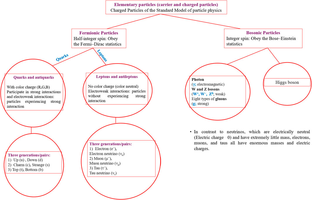
Figure 1. The elementary charged particles are summarized (CERN, 2024; Griffiths, 2008; Peskin and Schroeder, 1995; Krane, 1987; Navas et al., 2024; Kittel, 2005; Mann, 1955; The standard model of particle physics, 2007). Reproduced with permission (Nature, 448(7151), 2007). Copyright 2007, Springer Nature Publisher.
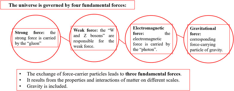
Figure 2. The four fundamental forces (CERN, 2024; Griffiths, 2008; Peskin and Schroeder, 1995; Krane, 1987; Navas et al., 2024; Kittel, 2005; Mann, 1955; Nature 2007). Reproduced with permission (The standard model of particle physics, 2007). Copyright 2007, Springer Nature Publisher.
Additionally, the electrons are considered slow since the optoelectronics are small. Frequent bumping, scattering, and heating occur among the transport of electrons; thus, Weyl fermions based on optoelectronics have many benefits. The current study examines alternative beam sources other than the conventional transport of electrons or optical types, such as antimatter and positron beam implementation, along with methods for producing electricity based on Weyl fermions. Introducing the positron and Weyl fermions’ interaction with the semiconductor is crucial in optoelectronics, which work by the movement of charge carriers between atoms. In Figure 3. Scientist’s work related to e+ in connection to some major progress in e+ physics (Zafar, 1990; Saud Abbas, 2024).
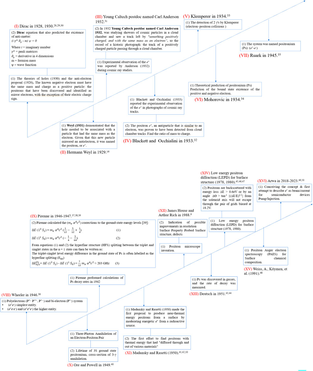
Figure 3. Pioneering work which is related e+ with years and references details to implement e+ towards semiconductor advancement (Zafar, 1990; Saud Abbas, 2024).
2 Electron and positron energy forms and distinguishable features of positrons and holes
2.1 Electrons and positrons
Fundamental particles categorized as leptons include electrons, which have a negative electric charge. The opposite of an electron is a positron. They are positively charged but have the same mass as electrons. Positrons are fermions and are similar to electrons in their quantum characteristics. However, gamma-ray photons can be produced when an electron and a positron collide and annihilate one another. The subatomic particles known as electrons and positrons have distinct characteristics and energy forms. A brief description of each is provided in Table 1.
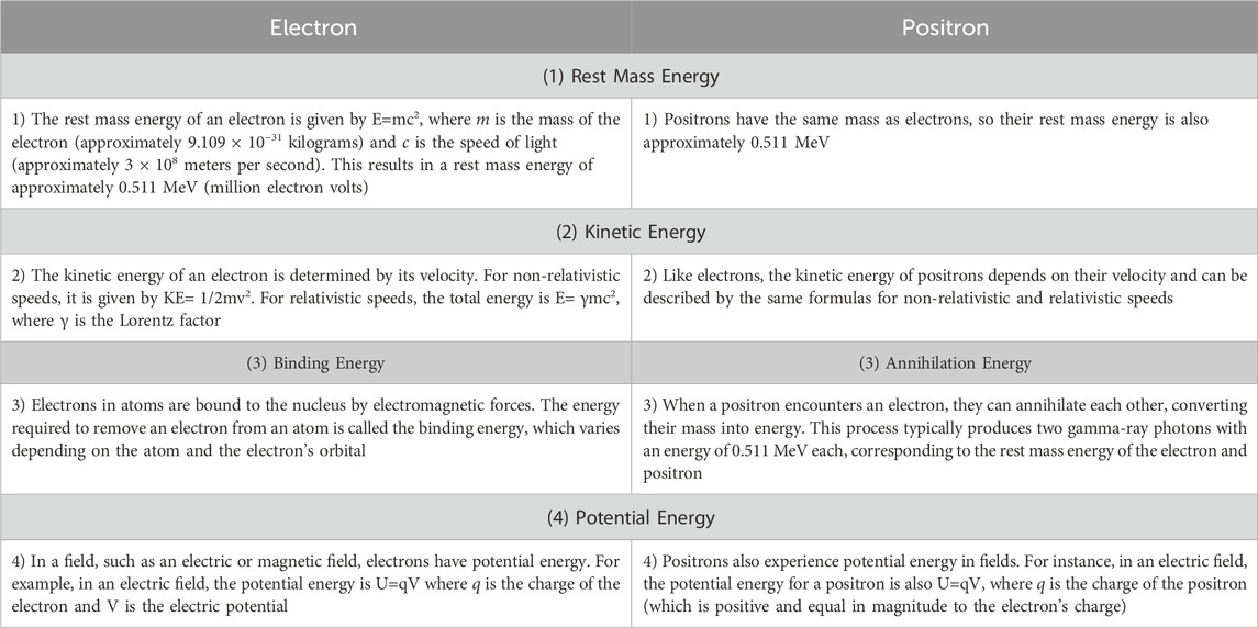
Table 1. The electrons and positrons have distinct characteristics and energy forms (Navas et al., 2024; Ahmed, 2015; Bertozzi, 1964; Elert, 1998-2024; Santhanam, 2018; Libretexts, 2024).
2.2 Positrons and holes
Although both particles—positrons and holes—carry positive charge, their origins and characteristics differ. These are the qualities that set them apart, as shown in Table 2. Positrons are real particles with a positive charge. They have equal mass to electrons, and they originate from particle interactions and decay processes. Positrons annihilate with electrons and are used as medical imaging or semiconductors defect investigations. Holes are quasi-particles representing the absence of electrons in semiconductors, and they have an effective positive charge and mass depending on the material. Holes are vital for the function of semiconductor devices (Griffiths, 2008; Krane, 1987; Navas et al., 2024; Kittel, 2005).
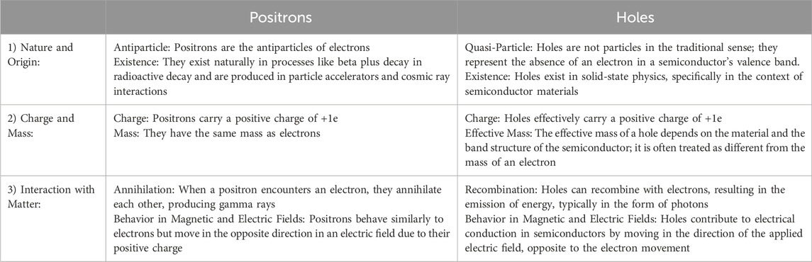
Table 2. The distinguishable features of positrons and holes (Navas et al., 2024; Kittel, 2005; Ahmed, 2015; Alvarez, 2013; Hemenway et al., 1967; Cross, 1978).
3 Working concept of positron in semiconductor devices
First, the antiparticle of electrons, known as positrons, is primarily employed in semiconductor devices for defect analysis using a method known as positron annihilation spectroscopy (PAS). Utilizing the special interactions between positrons and the electrical structure of the material, PAS offers insightful data regarding the defects present in the semiconductor (Krause-Rehberg and Leipner, 1999; Coleman, 2000). Second, positron sources are not realized for the majority of semiconductor carrier injection’s practical applications. An overview of the literature reveals that the primary practical uses of semiconductor carrier injection do not involve the utilization of positron sources or any other sources, such as Weyl fermions. Contributions to the flow of e+ could solve this problem. As shown in Figure 4, the process of activation of light emitters based-semiconductor involves (a) Injecting the devices with Lepton particles, and (b) Positron operation in semiconductor devices. This is a working concept for the generation of photons in semiconductors using other sources than e−.
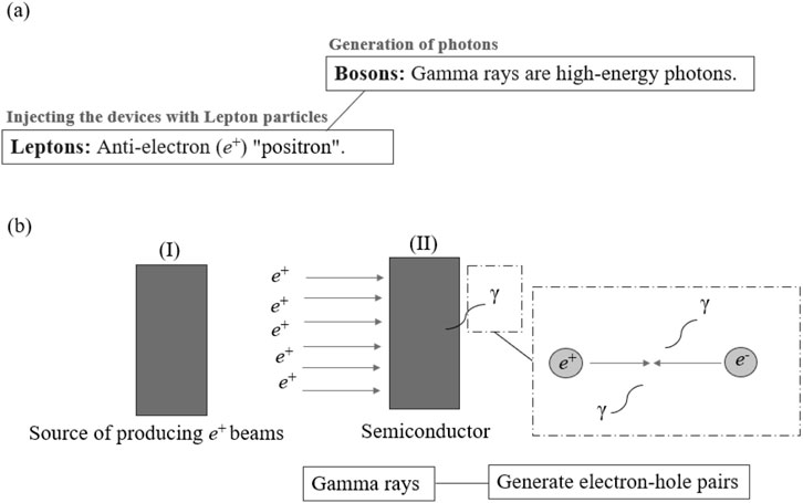
Figure 4. The process of activation of light emitters based-semiconductor: (A) Injecting the devices with Lepton particles, and (B) Positron operation in semiconductor devices; this is a working concept.
3.1 e+ beam source
The sodium-22 source, which emits β+, is the radioactive source (Van House and Rich, 1988) used to produce the positron beam in Figure 4. The positrons from this decay have a high energy of approximately 300 keV and have the potential to produce a slowing beam. James House et al. observed the interaction between approximately 2 eV e+ beam and the near-surface region of a solid, reporting e+ as the imaging particle (Van House and Rich, 1988). During this procedure, the high-energy (∼100–500 keV) source e+ thermalized in a crystal, such as a W crystal, and was expelled at an energy value of approximately 2 eV with a probability of 10−3–10–4. A beam is then created as a result of the ejected e+. The existence of the positron, the electron’s antimatter counterpart, has prompted a great deal of research into its behavior, especially in this recently-developed area of study on the properties of its interactions with a semiconductor. A positron beam source can be used in place of the electron emitter in a new generation of energetic source-driven semiconductor devices, which is their principal advantage. Mesons are often composed of a quark and an antiquark, while positronium is typically composed of an electron and a positron, and for the positron can be inelastically, or elastically backscattered towards annihilation or to be free positronium (Mills and Platzman, 1980). The positron and electron have similar masses and spins, but the positron’s charge has the opposite sign even if its magnitude is the same. Wide energy distribution positron sources up to high energies [keV-MeV] (Zafar, 1990) have been proposed for pumping and injecting semiconductor-based emitters based on a (Al,Ga)N material system. However, taking into account the evaluation of specific electron beam delivery must fall within the accepted range of eV values in order to prevent any damage that could result from the influence of e−/e+ beam irradiation on optical or electrical properties.
As the electron’s antimatter counterpart is readily accessible, there have been numerous studies conducted on the behavior of positrons as well as their production and application. The two techniques used to generate and use the positron beam emission—the laser-based source for electron and positron creation and the slow/fast positron beam technique—are essential to comprehending the behavior of the positron. As “slow positron moderators,” several materials are employed, such as thin single-crystal Ni(l00) and W(100) foils. The radioactive sources producing the rapid positrons have mean energies varying from several hundred keV to MeV (Zafar, 1990). Positron beam energy is comparable to electron beam energy. The starting point for the creation of positron beams is a sodium-22 source that emits β+. To regulate the positrons for use in further research, they must first be slowed down due to their high energy (300 keV) that results from their decay. The first findings were acquired using a transmission microscope equipped with the positron imaging particle. Similar to how electrons interact with matter, positrons’ interactions can reveal information about basic processes (Jmerik et al., 2023). The e+ generating radioactive source’s brightness, which is originally not high for imaging, can be increased by the process of moderation, which also boosts the instrument’s success (Mills et al., 1983; Schultz and Lynn, 1988). Heterostructure device development is based on the positron beam produced by a light emitter converting into positrons or the other potential process to convert an electron into a positron (Rosen, 2015).
3.2 The positron beam’s interactions with materials
In Figure 5, there is an obvious distinction between the electron and e+ images (Matsuya et al., 2011; Autjors Anonymous, 1924). To clarify the difference in imaging between e− and e+, e+ imaging process should be a similar working concept to e− as shown in Figure 6.
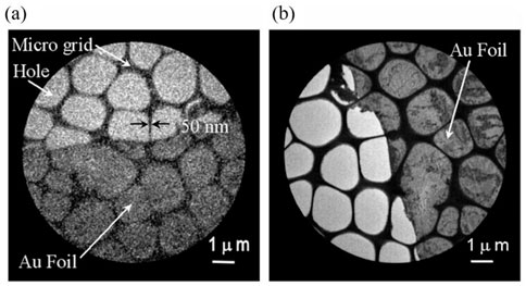
Figure 5. Transmission e− and e+ images of Au. (A) Imaged by positrons only. (B) Electron. Reproduced with permission (Matsuya et al., 2011). Copyright 2011, Elsevier Publisher.
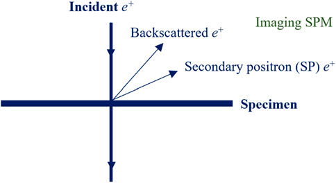
Figure 6. Schematic showing the similar workings of SEM as scanning positron microscopy (SPM) for imaging and the products of the interactions between the positron beam and the material such as the e+ backscattered (Mills and Platzman, 1980) and the secondary positron.
For the imaging principle:
• When the main e− in a scanning electron microscope (SEM) is targeted onto the material surface, various particles and waves are emitted, including photons, Auger e−, back-scattered e−, X-rays, secondary e−, etc.
• The imaging uses backscattered and secondary electrons, while the X-rays provide chemical details about the emitting atoms.
• Because the electron beam travels in a vertical direction via the microscope’s column, additional electrons are ejected from the sample as it comes into contact with it. The secondary or backscattered electrons are gathered by the detectors, which then transform them into a signal and send it to a viewing screen that resembles a regular television to produce a picture.
Rohrlich and Carlson et al. have demonstrated that, when using a transmission positron microscope (TPM), positron cross-sections could be greater than electron cross-sections. That indicates e+ with a certain energy range, a small scattering angle corresponds to a large scattering intensity. (Rohrlich and Carlson, 1954). Ultimately, significant variations between the e− and e+ diffraction contrast are predicted to transpire at energies of up to 1 MeV. (Ramamoorthy and Haji-Saeid, 2004; Hulett et al., 1984).
4 Massless particle for carrier transport in semiconductors
Weyl fermions are massless, highly mobile, and exhibit both matter-like and anti-matter behavior, in contrast to electrons (Kelly, 2015). The distinct characteristics of Weyl fermions, first proposed in 1929, may play a role in the development of quantum computers and rapid electrical circuits (Weyl, 1929). Hermann Weyl discovered an additinal solution to the Dirac equation which involved massless particles (Wang et al., 2017). Due to their fundamental characteristics, Weyl fermions travel rapidly on the crystal surface without backscattering, which in typical electronic materials increases heat rate and decreases efficiency. There are numerous benefits to using electronics with Weyl fermions. This is due to the requirement that an electron without mass move at the speed of light. Due to some spin features that are difficult to explain at this level, their transfer is faster and avoids colliding with objects. The distinct features of Weyl fermions are as follows:
1) Chirality: In terms of spin and motion direction, Weyl fermions are classified as left- or right-handed.
2) Massless: Weyl fermions are potentially massless in contrast to electrons and positrons.
3) Topology: Quasiparticles in some materials can exhibit Weyl fermionic behavior, giving rise to exotic phenomena such as the Weyl semimetal phase in which the conduction and valence bands touch at discrete locations known as Weyl points.
In 2013, Ling Lu et al. suggested that Weyl points physics, which is incorporated into condensed-matter physics, may also be achieved in photonic crystals. (Lu et al., 2013). Weyl quasiparticles exhibit non-trivial topological features and obey relativistic equations of motion, which partially protects them against scattering. Since Weyl fermions have no mass, Weyl fermions can transport electricity through a substance far more quickly than regular electrons. Faster optoelectronic devices might be created by utilizing this feature (Xu et al., 2015; Johnston, 2015; Jeffrey, 2015). The transformation to Weyl fermion is thought to transfer electric charge through a device significantly faster than that of regular electrons.
5 Conclusion and future work
In conclusion, I have taken the first attempt towards scientifically describing the utilization of the e+ and Weyl fermion in semiconductors. In view of the rapid developments in imaging analysis and slow e+ beam generation, there may be more opportunities to increase the use of positrons in semiconductor technology. Since this research will offer a distinct advantage for using other charged carriers instead of e− arising from this proposal, the upcoming years could be critical for furthering this technology. In light of the e+ and Weyl fermions’ potential application in the semiconductor industry, the beam sources should be developed to improve the efficiency of electronics and opto-electronic devices.
Data availability statement
The raw data supporting the conclusions of this article will be made available by the authors, without undue reservation.
Author contributions
AA: Conceptualization, Data curation, Formal Analysis, Funding acquisition, Investigation, Methodology, Project administration, Resources, Software, Supervision, Validation, Visualization, Writing–original draft, Writing–review and editing.
Funding
The author(s) declare that no financial support was received for the research, authorship, and/or publication of this article.
Conflict of interest
The author declares that the research was conducted in the absence of any commercial or financial relationships that could be construed as a potential conflict of interest.
Publisher’s note
All claims expressed in this article are solely those of the authors and do not necessarily represent those of their affiliated organizations, or those of the publisher, the editors and the reviewers. Any product that may be evaluated in this article, or claim that may be made by its manufacturer, is not guaranteed or endorsed by the publisher.
References
Ahmed, S. N. (2015). Elsevier Inc. Physics and engineering of radiation detection. doi:10.1016/C2013-0-15270-1
Alvarez, L. (2013). Introduction of the concepts of hole and effective mass using an alternative to the E-k diagram. Revista. Mexicana. de Física E 59, 128–132.
Autjors Anonymous (1924). Scanning electron microscopy and energy dispersive X-ray spectroscopy, chem 502 adv. Anal. Chem., Available at: https://web.iyte.edu.tr/∼serifeyalcin/lectures/chem502/L8.pdf.
Bertozzi, W. (1964). Speed and kinetic energy of relativistic electrons. Amer. J. Phy. 32 (7), 551–555. doi:10.1119/1.1970770
CERN (2024). The standard model. CERN Science. Available at: https://home.cern/science/physics/standard-model (Accessed September 10, 2024).
Coleman, P. G. (2000). Positron beams and their applications. Singapore: World Scientific Publishing Co. Pte. Ltd., 425. 9810233949.
Cross, R. C. (1978). Interpreting positive Hall voltages in terms of electron rather than hole motion. Amer. J. Phy. 46 (7), 771–772. doi:10.1119/1.11207
Elert, G. (1998-2024). Mass-energy. The Physics Hypertextbook. Available at: https://physics.info/mass-energy/ (Accessed December 21, 2024).
Griffiths, D. J. (2008). Introduction to elementary particles. 2nd ed. Weinheim: Wiley VCH, 480. 3527406018, 9783527406012.
Herrmann, P., Steinhauser, K.-A., Gähler, R., Steyerl, A., and Mampe, W. (1985). Neutron microscope. Phys. Rev. Lett. 54 (18), 1969–1972. doi:10.1103/physrevlett.54.1969
Hulett, L. D., Dale, J. M., and Pendyala, S. (1984). The generation of monoenergetic positrons and some potential applications in materials science. Mater. Sci. Forum 2, 133–150. doi:10.4028/www.scientific.net/MSF.2.133
Jeffrey, C. (2015). Available at: https://newatlas.com/massless-particle-weyl-fermion-princeton/38527/.
Jmerik, V., Kozlovsky, V., and Xinqiang, W. (2023). Electron-beam-pumped UVC emitters based on an (Al,Ga)N material system. Nanomaterials 13 (14), 2080. doi:10.3390/nano13142080
Johnston, H. (2015). Weyl fermions are spotted at long last. Available at: https://physicsworld.com/a/weyl.-fermions-are-spotted-at-long-last/.
Kelly, M. (2015). After 85-year search, massless particle with promise for next-generation electronics discovered. Princeton University. Available at: https://www.princeton.edu/news/2015/07/16/after-85-year-search-massless-particle-promise-next-generation-electronics.
Kittel, C. (2005). Introduction to solid state physics. 8th ed. Hoboken, NJ: Wiley, 704. 9780471415268.
Krause-Rehberg, R., and Leipner, H. S. (1999). Positron annihilation in semiconductors: defect studies. Berlin: Springer-Verlag, 387. 3-540-64371-0.
Libretexts (2024). S7.3: Electric potential and potential difference, Physics LibreTexts, Available at: https://phys.libretexts.org/Bookshelves/University_Physics/University_Physics_(OpenStax)/University_Physics_II_-_Thermodynamics_Electricity_and_Magnetism_(OpenStax)/07%3A_Electric_Potential/7.03%3A_Electric_Potential_and_Potential_Difference.
Levi-Setti, R. (1980) Adv. Electron. Electron phys. HIGH-RESOLUTION scanning transmissION LOW-ENERGY ION microscopes and microanalyzers, 13C, 261–320.
Levi-Setti, R., Crow, G., Wang, Y. L., Parker, N. W., Mittleman, R., and Hwang, D. M. (1985). High-resolution scanning-ion-microprobe study of graphite and its intercalation compounds. Phys. Rev. Lett. 54 (24), 2615–2618. doi:10.1103/physrevlett.54.2615
Lu, L., Fu, L., Joannopoulos, J., and Soljačić, M. (2013). Weyl points and line nodes in gyroid photonic crystals. Nat. Photonics 7, 294–299. doi:10.1038/nphoton.2013.42
Mann, R. (1955). University of Waterloo Ontario, Canada, an introduction to particle physics and the standard model. doi:10.1201/9781420083002
Matsuya, M., Jinno, S., Ootsuka, T., Inoue, M., Kurihara, T., Doyama, M., et al. (2011). Development of a transmission positron microscope. Nucl. Instrum. Methods Phys. Res. Sect. A Accel. Spectrom. Detect. Assoc. Equip. 645 (1), 102–112. doi:10.1016/j.nima.2010.12.228
Mills, A. P. (1983). “Enrico fermi,” in Positron solid state physics. Editors W. Brandt,, and A. Dupasquier (Amsterdam: North-Holland, International School of Physics “Enrico Fermi” Course), 1–16.
Mills, A. P., and Platzman, P. M. (1980). Observation of positron bragg reflection from Al and Cu surfaces. Solid State Commun. 35 (4), 321–324. Pergamon Press Ltd. Printed in Great Britain. doi:10.1016/0038-1098(80)90507-4
Navas, S., Amsler, C., Gutsche, T., Hanhart, C., Hernández-Rey, J., Lourenço, C., et al. (2024). Particle data group, review of particle physics. Phys. Rev. D. 110, 030001. Published 1 August 2024. Available at: https://pdg.lbl.gov. doi:10.1103/PhysRevD.110.030001
Peskin, M. E., and Schroeder, D. V. (1995). An introduction to quantum field theory. Boulder, CO: Westview Press, 864. 0201503972, 9780201503975.
Ramamoorthy, N., and Haji-Saeid, M. (2004) Industrial applications of radioisotopes and radiation technology and agency's role, in International atomic energy agency, Vienna, austri proceedings of the third eurasian conference nuclear science and its application, 5–8.
Rohrlich, F., and Carlson, B. C. (1954). Positron-electron differences in energy loss and multiple scattering. Phys. Rev. 93 (1), 38–44. doi:10.1103/PhysRev.93.38
Rosen, M. D. (2015). Transforming an electron into a positron: a new paradigm for physics. Harvard University. Available at: https://www.researchgate.net/publication/273318602_Transforming_an_Electron_into_a_Positron_A_New_Paradigm_for_Physics.
Santhanam, T. S. (2018). On a Generalization of Einstein’s E = mc2. J. Appl. Mathemat. Phy. 6, 1012–1016. doi:10.4236/jamp.2018.65088
Saud Abbas, A. (2024). Descripting e+ and Weyl fermion as beam/current for pump/injection semiconductor devices. Apl. Energy 1 (3), 030901. doi:10.1063/5.0203238
Schultz, P. J., and Lynn, K. G. (1988). Interaction of positron beams with surfaces, thin films, and interfaces. Rev. Mod. Phys. 60 (3), 701–779. doi:10.1103/revmodphys.60.701
Van House, J., and Rich, A. (1988). First results of a positron microscope. Phys. Rev. Lett. 60 (3), 169–172. doi:10.1103/physrevlett.60.169
Wang, S., Lin, B.-C., Wang, A.-Q., Yu, D.-P., and Liao, Z.-M. (2017). Quantum transport in Dirac and Weyl semimetals: a review. Adv. Phys. X 2 (3), 518–544. doi:10.1080/23746149.2017.1327329
Xu, S.-Y., Belopolski, I., Alidoust, N., Neupane, M., Bian, G., Zhang, C., et al. (2015). Discovery of a Weyl fermion semimetal and topological Fermi arcs. Science 349 (6248), 613–617. doi:10.1126/science.aaa9297
Keywords: positron and electron beams, positron-based laser setup, fermions and bosons, Weyl fermion-optoelectronics, and Weyl/Dirac fermions
Citation: Abbas AS (2025) Scientific explanation of e+ and Weyl fermion for injecting semiconductor devices. Front. Electron. 5:1372631. doi: 10.3389/felec.2024.1372631
Received: 23 March 2024; Accepted: 12 December 2024;
Published: 14 January 2025.
Edited by:
Abdus Salam Sarkar, Stevens Institute of Technology, United StatesReviewed by:
Subhashis Das, University of Arkansas, United StatesCopyright © 2025 Abbas. This is an open-access article distributed under the terms of the Creative Commons Attribution License (CC BY). The use, distribution or reproduction in other forums is permitted, provided the original author(s) and the copyright owner(s) are credited and that the original publication in this journal is cited, in accordance with accepted academic practice. No use, distribution or reproduction is permitted which does not comply with these terms.
*Correspondence: Arwa Saud Abbas, YXNhYmJhc0BrYWNzdC5nb3Yuc2E=