 Adwait Inamdar
 Willem D. Van Driel
 GuoQi Zhang
- Electronic Components Technology and Materials (ECTM), Microelectronics Department, Delft University of Technology, Delft, Netherlands
Electronic components are complex systems consisting of a combination of different materials, which undergo degenerative changes over time following the second law of thermodynamics. The loss of their quality or functionality is reflected in degraded performance or behaviour of electronic components, which can lead to failures during their operation lifetime. Thus, it is crucial to understand the physics of material degradation and the factors causing it to ensure component reliability. This paper focuses on the physics-of-degradation of packaging materials, which are typically exposed the most to the environmental and operating loads. The content of this article is organised into three parts. First, an overview of the packaging technology and encapsulating materials is presented. Then, the most common degradation-causing factors and package-associated failure modes are reviewed. Lastly, the hardware requirements are discussed, including specialised sensors, measurement techniques, and Digital Twins, to capture the degradation effects and facilitate component-level health monitoring for microelectronics.
1 Packaging technology
Electronic packages have evolved dramatically over the last 50 years, starting from the Dual In-line Package (DIP), Quad Flat Package (QFP), and Small Outline Package (SOP) in the early 1970s; then, the more efficient Leadless Chip Carrier (LCC), Pin Grid Array (PGA), and Ball Grid Array (BGA) packages in the 1980s to early 1990s; next, the smaller scale packages such as Quad Flat No-leads (QFN) and Chip-Scale Package (CSP) in the late 1990s; later, the multi-die packaging with System in Package (SiP) and Package on Package (PoP) in the 2000s; Wafer-Level Package (WLP) in the late 2000s; and finally, 2. XD (i.e., 2.1D, 2.3D, and 2.5D) and 3D integration in the 2010s and later (Lau, 2021; AnySilicon, 2011). In these components, electronic circuits and sub-components are encapsulated with different materials, such as ceramics, metals, and plastics, to form electronic packages.
The primary function of an electronic package is to protect the internal circuitry from external environmental and operating conditions that can potentially damage it or obstruct its proper functioning. Advanced packaging techniques provide high interconnect density and facilitate multi-layered, multi-functional heterogeneous integration. Thus, modern electronic packages are designed to also support signal transmission via interconnects, shielding electromagnetic interference (e.g., radio frequency applications), electric power distribution, thermal management, and heat dissipation (National Research Council, 1990; Lancaster and Keswani, 2018).
Several factors govern the performance and characteristics of an electronic package. For instance, the electrical performance is affected by the packaging delay, which depends on the type, complexity, and arrangement of the interconnects (Edwards, 2012; Lapedus, 2016). Moreover, the thermomechanical behaviour of an electronic package is also highly influenced by the thermal and mechanical properties of the encapsulating material, as it contributes to a large volume-share in a package (Phansalkar et al., 2022; Wei et al., 2009). Electronics packaging plays an important role in the functionality and useful life of an electronic assembly. Thus, the selection of an appropriate packaging material is crucial.
1.1 Encapsulating materials
An encapsulating material is required to have chemical stability, hydrophobic nature, thermomechanical properties in a certain suitable range, electrical insulation, thermal stability, and specific dielectric properties (Na et al., 2018). Historically, hermetic packaging with glass, ceramic, or metals (primarily the latter two) was commonly used for housing electronic circuits, making it up to 80% of worldwide microcircuit production in the 1960s. Emerging as an inexpensive alternative in the 1970s, plastic packaging took over virtually all high-volume packaging products, acquiring 97% of the total market share in 1993 and more than 99% by the year 2000. Due to this large-scale adoption, polymer-based compounds have dominated the packaging market in the last 2 decades [(Ardebili et al., 2018, ch.1)]. Figure 1 summarises the timeline of two competing packaging technologies, with all hermetic packaging materials classified as one category.
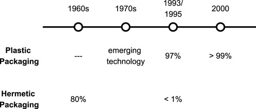
Figure 1. The evolution of the per cent (%) market share of packaging materials in the commercial microelectronic devices. Plastic-based packaging became the default for most applications (
Thermosetting polymers such as epoxy, polyimide, bismaleimide-triazine, etc. are widely used in packaging materials because of their low dielectric permittivity (Li et al., 2022). Owing to their ability to be moulded, they are also referred to as “moulding compounds.” Their relatively low cost compared to traditional ceramic packages and also comparable reliability make them a more practical choice for packaging. There is a wide variety of resins suitable for Plastic-Encapsulated Microelectronicss (PEMs) (Ardebili et al., 2018, ch.2), (Charles, 1993). Considering the superior electrical performance, achievable thermal and mechanical behaviour, and economical aspects, the use of epoxy-based plastics is widespread for commercial electronic devices (Pecht et al., 1999).
1.2 Epoxy moulding compounds
A typical Epoxy Moulding Compound (EMC) is a composite material, utilizing epoxy resin as a matrix along with silica-based filler material and other additives. A wide range of thermomechanical properties can be achieved by varying the quantities of the fillers and additives (Carolan et al., 2016; Kandola et al., 2010). For example, the glass transition temperature
The constitutive materials of EMC help it attain the desired thermomechanical properties. The epoxy resin contributes to excellent chemical resistance, weight reduction due to its lower density, as well as high adhesion strength due to the formation of hydroxyl groups during cure (Na et al., 2018; Mullins et al., 2012). Typically, EMC has a very high filler content (up to 90%), which helps reduce the Coefficient of Thermal Expansion (CTE) and increase the thermal conductivity of the moulding compound (Ardebili et al., 2018, ch.2). It also improves dimensional stability with the resulting low shrinkage and high
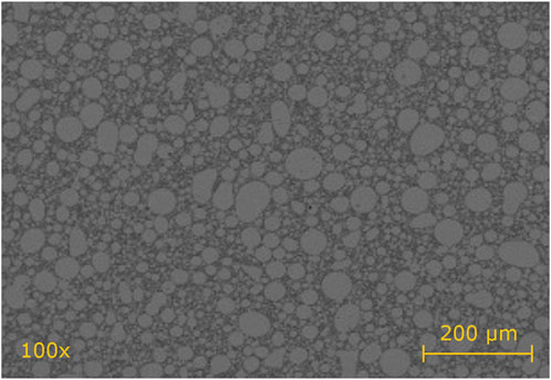
Figure 2. A cross-section of an EMC specimen observed under an SEM. The light grey region indicates the
The silica-based filler also ensures the reduction of moisture absorption (Sasajima et al., 2016) and of the large CTE-mismatch between silicon die (2–3 ppm/°C) and epoxy resin (above 80 ppm/°C), ensuring less warpage (Teh et al., 2006). The
2 Package-associated degradation
The encapsulating material occupies a large volume within a package [as high as 75% (Liu, 2012)]; thus, it is most exposed to external environmental conditions. It is not only true for simple single-chip packages but also for complex multi-chip packages such as PoP, SiP, and 3D integration. Figure 3 illustrates several options for modern electronics packaging. In all of the examples, a high volume-share of the encapsulating material is observed.
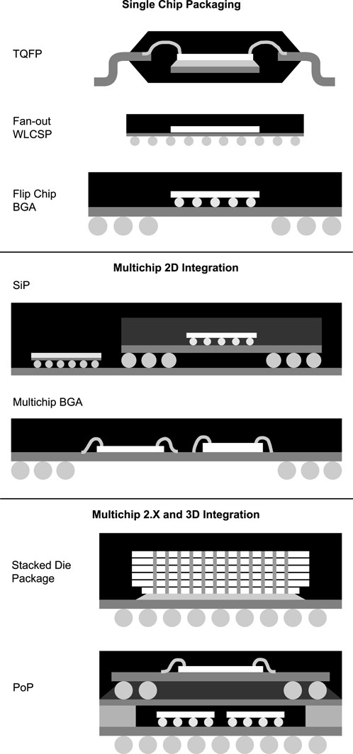
Figure 3. A schematic representation of different options for electronic packages, classified into three categories–single-chip packages, multi-chip 2D integration, and advanced 2.X and 3D integration. All options indicate the encapsulating material in black colour, which also has a dominant volume-share.
This trend is seen throughout the history of electronics packaging (1970s–2000s) and also the advancements in the recent past, reviewed in numerous publications (Lancaster and Keswani, 2018; Ardebili et al., 2018; Liu, 2012; AnySilicon, 2011; Greig, 2007; Zhang and Lu, 2016; Perfecto and Srivastava, 2013; Lau, 2021). Although most Wafer-Level Chip-Scale Packages (WLCSPs) do not have a plastic encapsulation (NXP Semiconductor, 2015; Qu and Liu, 2015), such WLCSPs get encapsulated after being integrated into a larger system (e.g., a SiP). This is illustrated in Figure 3 with a Fan-in WLCSP on the left-hand side portion of the package labelled as “SiP.” Thus, the encapsulation material is a dominant part of an electronic package. It is exposed the most to the surrounding environment and, thus, is prone to degradation and ageing.
2.1 Degradation factors
The factors responsible for component degradation can either be “environmental” or “functional” loads. The former depends on aspects such as the geographic location, season, and time of the day, while the latter on the application field and operating conditions such as the power requirement, runtime, etc. These factors can be categorised into eight types–thermal, electrical, mechanical, chemical, electromagnetic, radiation, humidity, and dust (ZVEI, 2015). Among these, harsh conditions such as high temperature, moisture, and mechanical vibrations have the most relevance for electronic components in a broad variety of applications. Exposure to these “stress-factors” alters the thermal, mechanical, electrical, and chemical behaviour of the constituting materials, which influences the performance, behaviour, and lifetime of an electronic component. Figure 4 indicates the distribution of the share of four major “stress-factors” in causing failures in electronic components.
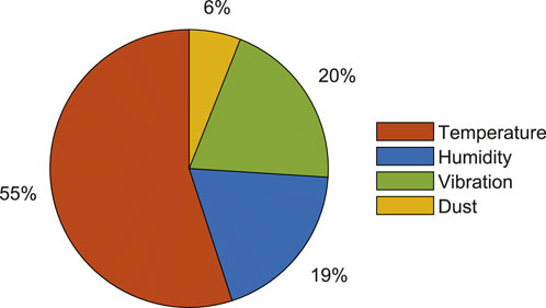
Figure 4. Four key “stress-factors” responsible for causing failures in electronic components–temperature, humidity, vibration, and dust. The pie chart indicates the percentage share of each factor in failures (Pecht, 1991; Chu et al., 2013; Xu et al., 2015; Qiu et al., 2022).
The data originates from a 1990 study by the US Air Force Avionics Integrity Program, which has later been reported on in handbooks such as Pecht (1991) and a variety of publications on the studies of different failure modes in electronics packages (Chu et al., 2013; Xu et al., 2015; Qiu et al., 2022). Temperature is the most significant stress-factor (accounting for more than 50%) to facilitate failure mechanisms in electronic components, while humidity and mechanical vibrations are the next two dominant ones. Failure mechanisms are also often accelerated by these factors, and thus, the knowledge of the exposure of an electronic component to the dominant stress-factors is crucial in determining its current state of degradation and predicting a potential failure mode.
In addition to these factors, exposure to gas (chemical exposure), salt (corrosion), ultraviolet light (ageing effects), electromagnetic radiation, power surges (electromigration), etc. have also been considered as a part of the reliability qualification tests in the recent past (ZVEI, 2015; ITA Labs, 2014; Sierra Circuits, 2021). However, the relevance of these additional factors remains application-dependent, keeping the aforementioned four stress-factors as almost exclusively cited degradation factors in a plethora of publications to date. The modern trends in reliability testing for microelectronics packaging also reflect the same (Bender et al., 2024).
Each of the dominant stress factors has certain degradation effects and associated failure mechanisms. Exposure to high temperature leads to oxidation of the encapsulating moulding compound, which is a chemical reaction leading to the formation of a stiffer layer compared to the original material (Inamdar et al., 2021). A PCB substrate also shows a similar degradation effect with a significant shift in its mechanical properties (Van Dijk et al., 2022; van Dijk et al., 2024). High temperature also accelerates the creep in solder joints, leading to a significant shift in its material properties and, thus, its mechanical behaviour (Lall et al., 2024; Mazumder et al., 2024). Thermal cycling and thermal shocks also have unique effects on the die-attach layer (which sits between the die and substrate for certain packaging configurations) and solder joints, leading to fatigue (Fahim et al., 2019; Abueed et al., 2019).
Humid environments can cause hygroscopic swelling of encapsulating moulding compounds due to moisture diffusion (Kwak and Park, 2015; Teverovsky, 2002; Jansen et al., 2020), which reflects in a change in thermomechanical behaviour (Zulueta et al., 2021). This effect, in particular, is partially reversible through the desorption of moisture, since it is a diffusion-dominated physical phenomenon (Placette et al., 2011; Chen et al., 2015). This degradation primarily leads to delamination, bond wire failure, and cracks in substrates, encapsulation, and solder joints (van Driel et al., 2010). A combination of thermal and humidity loads results in adhesion failure of moulding compounds (Ahsan and Schoenberg, 2014) as well as the “popcorning” effect in electronic packages (Chen and Li, 2011). Hygrothermal exposure causes a combination of physical and chemical degradation effects and has a significant influence on die-level mechanical stresses (Nguyen et al., 2018), which can lead to interfacial delamination (Wang and Wu, 2020).
Mechanical vibrations impose repetitive mechanical stresses on several layers within an electronic package or system (Thukral et al., 2024b). The effects of such a loading condition are heavily reflected in fatigue failure of solder joints (Wang et al., 2017; Libot et al., 2016) and can depend on the magnitude of vibration in a particular direction (Jian et al., 2024). These effects are typically accelerated under thermal loads and thus, a combined degradation due to thermal and mechanical stress has been extensively studied and characterised (Maruf et al., 2024; Arabi et al., 2020) and several board-level reliability studies are designed around solder fatigue under thermal-cyclic and mechanical vibratory loads (Bani Hani et al., 2023; Thukral et al., 2023; An et al., 2018).
The aforementioned stress-factors and corresponding degradation mechanisms and failure modes are applicable to different electronic packages depending on the utilised packaging technology. Simpler chip designs (single chip packaging in Figure 3) can experience a single dominant failure mode, such as wire-bond liftoff or popcorning effect. On the other hand, multi-chip 2D integration or advanced packaging (refer to the rest of Figure 3) have more complex structures and, thus, the complex interaction of multiple layers consisting of different materials. This leads to a combination of failure modes including solder interconnects at different layers, electromigration, and substrate cracking. Bernstein et al. (2024) shows the distribution of most commonly observed package-level failure mechanisms in the field as bond wire failure (32%), die cracking or damage (28%), delamination (13%), substrate cracking (10%) among others. These failure modes are identified using several Highly Accelerated Stress Testing (HAST) and cyclic loading profiles, which are based on temperature variation (thermal cycling, shock, isothermal), humid environments (moisture ingress), and mechanical loads (vibrations) (Bender et al., 2024).
2.2 Failure modes
Package-level degradation mechanisms can lead to both package-level failures as well as board-level failures. Figure 5 shows the distribution of different types of package-level and board-level failure modes associated with power electronic systems. The original source (Wolfgang, 2007) is not accessible, but the data were later reproduced in Yang et al. (2010) and Wang et al. (2012). The package-associated failure modes–semiconductors (die), connectors (interconnects), and solder joints–together account for a significant share of 37%. In general, there can be a large number of failure modes for an electronic component or system [(Ardebili et al., 2018, ch.5)]. Thus, a selection is necessary to focus the efforts on modelling the physics-of-degradation and building a physics-based Digital Twin for prognosis. The following three criteria were considered to determine the dominant failure modes and degradation mechanisms: (1) the three dominating stress-factors (viz., temperature, humidity, and vibration); (2) the large volume-share of the encapsulation material with a dominant role in the thermomechanical behaviour of a package; and (3) the trend of commonly observed categories of package-associated failures.
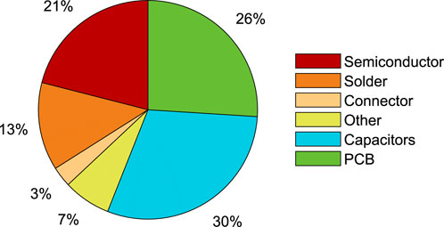
Figure 5. The distribution of failure modes associated with different sub-components of power electronic systems based on the data presented in Wolfgang (2007), Yang et al. (2010), Wang et al. (2012). The failures related to the semiconductor (die), connector (interconnects), and solder joints together account for over a third of total failure modes.
Delamination, i.e., separation of two heterogeneous surfaces, and cracking of materials are two of the most common mechanical failure mechanisms. Delamination is often observed at the interfaces between the moulding compound and other materials, such as EMC-leadframe, EMC-die, etc. Delamination can also lead to crack propagation in the bulk of EMC. Figure 6A shows the schematics of these failure modes, which are mainly caused by the difference between the thermomechanical properties (e.g., CTE-mismatch) and temperature differences between different layers. A cyclic thermal load during the component’s operation causes stress cycling which leads to crack initiation and propagation. Delamination can affect not only the electrical performance but also the thermal performance by altering the heat distribution within the package (Nieuwenkamp and Bosco, 2021).
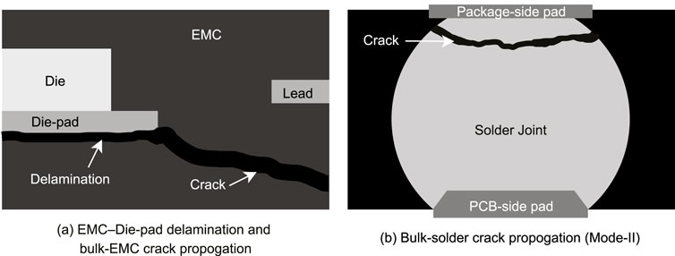
Figure 6. Examples of package-associated failure modes – (A) delamination of EMC-leadframe interface and cracking of bulk-EMC and (B) crack propagation in the bulk of a solder joint. Both failure modes are initiated by fatigue load and accelerated by thermomechanical degradation of EMC.
A cyclic thermal or mechanical load is also a primary cause of crack initiation and propagation within solder joints. Figure 6B depicts a crack in the bulk of solder material, which is also referred to as a Mode-II failure. Solder cracks can also develop within the intermetallic layer formed up to a certain depth from its contact with the metallisation (commonly copper) layer. This is called a Mode-I failure. The former is a predominantly ductile failure due to plastic deformation (i.e., the accumulated plastic strain), while the latter is a brittle failure. A mixed-mode failure can also be observed in solder joints. Both of the described failure modes (illustrated in Figure 6) have one common factor, which is they occur during product-operation, i.e., the in-use phase of an electronic product. Moreover, they can be accelerated by the changed thermomechanical behaviour of a package due to the ageing of the encapsulating EMC. Thus, the changes in material properties of the encapsulating material are of great significance when considering the effects of package-level degradation on the component-level failure modes.
3 Degradation monitoring and reliability
The reliability of a component refers to its future performance or behaviour, which inherently has the uncertainty and randomness involved (Kapur and Pecht, 2014). Thus, the mathematical formulation of reliability is a function of the random variable
This approach, being in use since the 1960s, has been heavily criticised in the past for being inaccurate and invalid because of being based on insufficient knowledge of component failures (Pecht and Kang, 2018). It has also been highly recommended to replace them with newer approaches, e.g., physics-of-failure (PoF). In addition, it provides only a collective overview and broader insights into an entire batch using a statistical approach, which also implies that it lacks the details of sample-specific insights. Methods of reliability estimation have evolved quite a lot from the birth of fault-tree analysis in the 1970s, the use of accelerated testing in the 1980s, the adoption of the physics-of-failure approach in the 1990s, to the hybrid approach using physics and statistics together (Azarkhail and Modarres, 2012; Wang and Blaabjerg, 2021).
The methodology needs to further develop to match the needs created by the next-generation and rapid electronification of industries and involvement of mission critical electronics. It should provide per-product (sample-specific) health monitoring but at a much larger scale, possibly for all the products (not just a smaller sample set) while they are in use. The industries are expected to move from an “application-based” to a “degradation-based” wave in reliability in the near future (van Driel et al., 2022), which means the focus would transition from a physics-of-failure to a physics-of-degradation approach to estimate a product’s service lifetime or its Remaining Useful Life (RUL).
In the physics-of-failure approach, the focus is on failure mechanisms and understanding the physics behind them. For instance, the mechanics behind the development of cracks due to solder fatigue under a cyclic load is the main focus. In a physics-of-degradation approach, the focus is on understanding the physics behind the change of state from nominal to degraded, until failure. Thus, this approach is aimed at capturing more information on the intermediate stages of degradation before failure. An example is presented in Thukral et al. (2024a), where four different stages of solder joint degradation are identified based on the four-point resistance measurement technique. These stages appear before the crack (i.e., the failure mode) actually starts to develop. Thus, a physics-of-degradation approach provides far more detailed information on the degradation and failure phenomena.
This approach can be realised using a Digital Twin-based framework for Prognostics and Health Management (PHM) of electronics. Figure 7A indicates the two-branched Digital Twin model, which leverages two modelling approaches–physics-based and data-driven. The model keeps a clear separation between the real and virtual spaces, and either one of these two branches can be the digital model on its own to provide a prognosis while forming a closed feedback loop with the physical product. Furthermore, the two modelling approaches can be combined to a varied capacity to get a hybrid Digital Twin. A Digital Twin implementation can exist in three forms, viz., Digital Twin Prototype (DTP), Digital Twin Instance (DTI), and Digital Twin Aggregate (DTA), during different phases of product lifecycle Grieves (2023). The last one refers to the in-use phase and facilitates component-level (product-specific) health monitoring at scale. An expanded version of the two-branched model and its workflow throughout a product life-cycle has been described in great detail in Inamdar et al. (2024b).
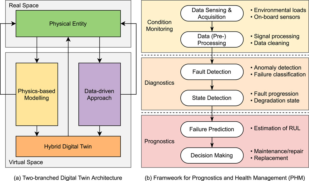
Figure 7. The two-branched Digital Twin architecture that leverages two modelling approaches (viz., physics-based and data-driven) and the six-step framework for PHM of microelectronics. The two branches of the digital models can be combined for a hybrid approach to component-level degradation monitoring. (A) Two-branched Digital Twin Architecture (B) Framweork for Prognostics and Health Management (PHM).
Figure 7B summarises the six-step framework for component-level PHM and degradation monitoring. The workflow of PHM begins with condition monitoring, which requires the collection of relevant data using appropriate sensors for capturing environmental loads, operating conditions, and additional measurements (e.g., current or voltage). Thus, the first three steps in the PHM workflow are data sensing, acquisition, and preprocessing. The second phase of the PHM framework is diagnostics. The collected data is processed to provide a preliminary assessment of the component’s condition, such as the detection of an anomaly. The state of component health is then evaluated, which requires physics-based validated models for quantifying degradation and fault progression. In the last phase, prognostics and decision-making come into the picture. A prognosis of the component’s performance and an estimation of its RUL is made. Based on the prediction, decisive action is chosen, such as scheduling maintenance for repair or replacement.
3.1 Hardware for degradation monitoring
Product-specific health monitoring and reliability prediction can be achieved when its exposure to the dominant stress-factors is known, which can be used to determine the current state of degradation. This requires incorporating embedded sensors and component-level measurement techniques in an electronic system. Thus, certain hardware considerations are necessary to realise the data-driven branch of the Digital Twin architecture presented in Figure 7A, especially the edge-processing aspect, and to establish the data flow from the physical product and its digital models in the virtual space. This is important for the “instance” (DTI) and crucial for the “aggregate” (DTA) phase of the Digital Twin. The hardware requirements are categorised into sensing and processing units.
3.1.1 Sensors and measurements
A set of sensors to measure temperature at various locations of a component, moisture content in the surroundings, and certain aspects of mechanical vibrations is the basic necessity. Multiple locations to measure the temperature are recommended. A measurement outside a package records the environmental (i.e., external temperature), while the ones within a component can measure the effects of joule heating due to the active power cycling. Moreover, a failure mode such as delamination could also be monitored as it affects the heat distribution. An example of temperature sensor-based prediction of the EMC-die delamination has been presented in Nieuwenkamp et al. (2023). A temperature sensor also helps in estimating the stresses when it is linked with a physics-based model such as a Finite Element model. Additional analogue sensors and external thermocouples can also serve to monitor the temperature at a specific location.
Moisture diffusion into EMC affects the mechanical behaviour of the encapsulation layer and, in turn, of the whole package (Sugiman et al., 2016). Relative humidity (%RH) measurements aided with an atmospheric pressure sensor can help quantify these effects. Humidity and temperature both affect the thermomechanical properties of EMC. Thermal ageing produces permanent oxidative changes, whereas the effects of moisture diffusion are reversible to a certain extent (Netting, 2012). Thus, real-time and accurate humidity measurements are crucial to accumulating moisture-induced effects on the mechanical behaviour.
Mechanical vibrations are a common source of the dynamic operating load for electronics in the automotive and manufacturing field. It causes stress cycling, leading to fatigue failures such as delamination and cracking due to cumulative damage of the EMC-die interface (package-level) and solder fatigue due to accumulated plastic strains (board-level). Linear motion is sensed by a 3-axis accelerometer, while angular motion is by a 3-axis gyroscope. A standard 6-axis Inertial Measurement Unit (IMU) (or a 9-axis IMU which includes a 3-axis magnetometer for the orientation in space) should be integrated at one or more locations to record the vibration load at the component- or board-level.
Apart from the individual effects of the stress-factors, it is also crucial to see the effect of coupled loading because such loads represent a more realistic scenario and generally have a greater influence on the acceleration of failure modes. Several publications indicate this by studying the effect of coupling temperature-humidity (Wang and Wu, 2020; Jansen et al., 2020; Zulueta et al., 2021) and temperature-vibrations (An et al., 2018; Arabi et al., 2020). Some ageing and degradation processes can have much longer characteristic times than the operation times of the device (Swingler and Feinberg, 2014, ch.3). Thus, the frequency of measurements should be tweaked according to the target failure mechanisms and the involved physics-of-degradation.
In addition to capturing the effects of the dominant stress-factors, specialised sensors and measurement methods can be implemented to get additional information about the state of degradation. For instance, electrical resistance measurements can identify a failed solder joint and also a few degraded stages before failure (Zhang, 2023, ch.4), as well as effects such as electromigration. Measurements from a piezoresistive sensor can represent the changes in stresses and indicate the progress of degradation or damage. Some examples of this have been demonstrated in Prisacaru et al. (2021), Prisacaru and Gromala (2021), Inamdar et al. (2024a).
3.1.2 Processing and communication
Data collection through sensors requires a controlling on-board unit, which a Microcontroller Unit (MCU) along with a multiplexer (or “mux”) can fulfil. The MCU needs to be selected so that some data processing can be done on the edge. The advantages of this are twofold – (1) high quality data can be directly processed without it leaving the device, and only the inference can be stored or transmitted. This is also a more secure option with respect to data privacy; and (2) it simplifies the workflow while saving a lot of energy by avoiding at least a part of data stream transmissions, which inherently has high energy consumption (Warden and Situnayake, 2019; Edge Impulse, 2021).
ARM-based architecture for processors is known for its energy efficiency and also provides a wide variety of high and low-power compute cores. Their “M” series of designs have limited compute power compared to the “A” series but are energy efficient, making them suitable for in-situ health monitoring. ARM recommends several tiers of processing units (xPUs) for data processing across different use cases (Vachani, 2020). The in-situ health monitoring implementation requires making sense of the data coming from different sensors or multiple sensors of the same kind (i.e., sensor fusion) and having embedded Machine Learning (ML) capabilities such as feature extraction, failure classification, and anomaly detection. Thus, at the least, Cortex M7 or equivalent compute architecture should be selected.
Since the computational power available at the edge (MCU) has its limitations, some sorts of data analysis (e.g., federated learning) can only be done on an external system (or cloud). This can be achieved by wireless communication interfaces such as WiFi and Bluetooth Low Energy (BLE). Wireless connectivity is also paramount for maintaining a continuous feed of sensor data to continuously update the physics-based model in the cloud. For transmitting data to a locally available but external computation infrastructure, connections for wired communication channels such as SPI and I2C should be available on the board-level. A USB interface or a dedicated port might also be necessary for data transfer and software/firmware updates. Finally, flash memory solutions can be considered for local storage of processed data and inferences.
3.2 Virtual sensors and Digital Twins
Predicting failures directly from the collected sensor data is not possible without a robust (purely) data-driven model, which typically requires huge amounts of training data gathered from experiments or in-field use of the product. The hybrid Digital Twin approach for prognostics and health monitoring of electronics (Figure 7) can address this challenge, and thus, linking the sensor data to physics-based models is necessary. Experimentally validated models can then also serve as a source for training data that is convenient and not as resource-intensive as a purely experimental approach. Moreover, these models can extract results from intricate places of the electronic component, serving as “virtual sensors,” where placing and physical sensor or performing actual measurements is either not possible or practical.
As concluded in Section 2, temperature-induced effects on the encapsulating layer of an electronic package are crucial. Thermal ageing results in progressive oxidation of the encapsulating EMC, forming a much stiffer outer layer. This affects the stresses on the EMC-die interface and may accelerate the delamination process. While embedding a piezoresistive stress sensor is a possible solution, it is also resource-intensive. As an alternative, an experimentally validated model of a thermally aged electronic package can be prepared to simulate its thermomechanical behaviour as a function of EMC oxidation. A step-by-step procedure of creating such a continuously updated and experimentally validated model for thermo-oxidative ageing of EMC is demonstrated in Inamdar et al. (2024c). This model can serve as a virtual sensor to extract the stress values along the EMC-die interface to evaluate the risk of delamination.
Figure 8 shows the aforementioned model with a quarter geometry of a flip-chip ball grid array package, that updates the thickness and material properties of the oxidized layer of EMC based on the quantified exposure (i.e., time) to a high temperature (
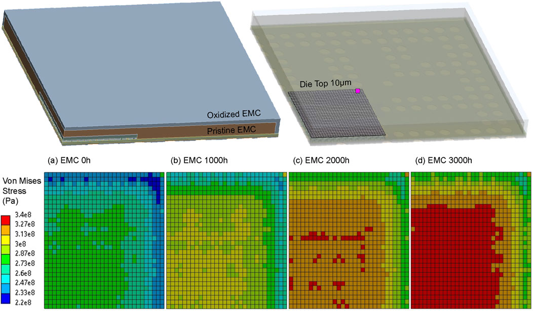
Figure 8. An example of implementing a virtual sensor for extracting stress along the EMC-die interface as a function of thermal ageing of an electronic package. The plots indicate the von Mises equivalent stress at room temperature for four different levels (hours) of EMC oxidation due to exposure to high temperature. (A) EMC 0 h (B) EMC 1,000 h (C) EMC 2,000 h (D) EMC 3,000 h.
4 Conclusion
This paper reviews the state of the art of electronics packaging and materials used for encapsulation. It shows that over 99% of commercial electronics utilise plastic encapsulation with epoxy-based moulding compounds being a popular choice. The encapsulation layer retains a dominant volume-share in several types of conventional or advanced packages and, thus, is a critical layer when package-level degradation and associated mechanical failure modes are concerned. Exposure to temperature, moisture, and mechanical vibrations influences the package-associated failure mechanisms, among which delamination and solder fatigue are two of the most commonly identified failure modes.
Dominant stress-factors have their individual effects on material degradation that lead to the acceleration of failure modes. However, it is also crucial to study the coupled effects, as they represent more realistic loading conditions. Thus, multi-physics superposition is necessary when preparing a physics-based Digital Twin model. In addition, a set of sensors and measurement techniques should be in place to achieve component-level, continuous, and in-situ condition monitoring. The advantages are twofold – (1) it can be utilised to update the physics-based model in the cloud to represent the current state of degradation, and (2) the data can be processed in-situ using sensor fusion and ML for quantification of degradation parameters, failure detection, and classification of failure modes.
The additional hardware required to realise in-situ component-level health monitoring can be categorised into sensing and processing units. The selection of suitable computing hardware, such as an MCU, depends on the required computational power and the necessary energy efficiency at the edge. Apart from the sensors for measuring the basic environmental loads, the inclusion of additional specialised sensors, such as a piezoresistive sensor, provides more insights into the progressive degradation of electronic components. In addition to the hardware sensors, Digital Twin-based virtual sensors serve as a more practical solution for gathering data. Thus, experimentally validated physics-based degradation models are a crucial aspect in realising a hybrid approach to component-level PHM of electronics.
Author contributions
AI: Conceptualization, Formal Analysis, Investigation, Methodology, Visualization, Writing–original draft. WV: Conceptualization, Funding acquisition, Project administration, Supervision, Writing–review and editing. GZ: Conceptualization, Funding acquisition, Supervision, Writing–review and editing.
Funding
The author(s) declare that financial support was received for the research, authorship, and/or publication of this article. A part of this work has been carried out within the ArchitectECA2030 project under the grant agreement No. 877539. The project is co-funded by grants from Germany, Netherlands, Czech Republic, Austria, Norway, and Electronic Component Systems for European Leadership Joint Undertaking (ECSEL JU).
Conflict of interest
The authors declare that the research was conducted in the absence of any commercial or financial relationships that could be construed as a potential conflict of interest.
Generative AI statement
The author(s) declare that no Generative AI was used in the creation of this manuscript.
Publisher’s note
All claims expressed in this article are solely those of the authors and do not necessarily represent those of their affiliated organizations, or those of the publisher, the editors and the reviewers. Any product that may be evaluated in this article, or claim that may be made by its manufacturer, is not guaranteed or endorsed by the publisher.
References
Abueed, M., Alathamneh, R., Suhling, J., and Lall, P. (2019). “Effect of creep and fatigue on individual SAC305 solder joint reliability in isothermal cycling,” in SMTA international conference proceedings.
Ahsan, T., and Schoenberg, A. (2014). “Investigation of the mechanisms of adhesion and failure in microelectronic packages,” in Adhesion in microelectronics. Editors K. Mittal, and T. Ahsan (John Wiley and Sons, Ltd), 9781118831, 313–341. doi:10.1002/9781118831373.CH8
An, T., Fang, C., Qin, F., Li, H., Tang, T., and Chen, P. (2018). Failure study of Sn37Pb PBGA solder joints using temperature cycling, random vibration and combined temperature cycling and random vibration tests. Microelectron. Reliab. 91, 213–226. doi:10.1016/J.MICROREL.2018.10.003
Arabi, F., Gracia, A., Delétage, J. Y., and Frémont, H. (2020). Effect of thermal and vibrational combined ageing on QFN terminal pads solder reliability. Microelectron. Reliab. 114, 113883. doi:10.1016/J.MICROREL.2020.113883
Ardebili, H., Zhang, J., and Pecht, M. G. (2018). Encapsulation technologies for electronic applications. second edn. Elsevier. doi:10.1016/C2016-0-01829-6
Azarkhail, M., and Modarres, M. (2012). The evolution and history of reliability engineering: rise of mechanistic reliability modeling. Int. J. Perform. Eng. 8, 35. doi:10.23940/IJPE.12.1.P35.MAG
Bani Hani, D., Al Athamneh, R., Abueed, M., and Hamasha, S. (2023). Reliability modeling of the fatigue life of lead-free solder joints at different testing temperatures and load levels using the Arrhenius model. Sci. Rep. 2023 13 (1), 2493–2513. doi:10.1038/s41598-023-29636-3
Bender, E., Bernstein, J. B., and Boning, D. S. (2024). Modern trends in microelectronics packaging reliability testing. Micromachines 15, 398–415. doi:10.3390/MI15030398
Bernstein, J. B., Bensoussan, A. A., and Bender, E. (2024). Reliability prediction for microelectronics. Hoboken, NJ: wiley. doi:10.1002/9781394210961
Carolan, D., Ivankovic, A., Kinloch, A. J., Sprenger, S., and Taylor, A. C. (2016). Toughening of epoxy-based hybrid nanocomposites. Polymer 97, 179–190. doi:10.1016/J.POLYMER.2016.05.007
Charles, H. K. (1993). Materials in electronic packaging at APL. Laurel, MD: Johns Hopkins APL. Technical Digest 14.
Chen, L., Chu, H. W., and Fan, X. (2015). A convection–diffusion porous media model for moisture transport in polymer composites: model development and validation. J. Polym. Sci. Part B Polym. Phys. 53, 1440–1449. doi:10.1002/POLB.23784
Chen, Y., and Li, P. (2011). “The “popcorn effect” of plastic encapsulated microelectronic devices and the typical cases study,” in ICQR2MSE 2011 - proceedings of 2011 international conference on quality, reliability, risk, maintenance, and safety engineering, 482–485. doi:10.1109/ICQR2MSE.2011.5976658
Chu, R. C., Simons, R. E., Iyengar, M., and Yeh, L.-T. (2013). “Thermal management of flip chip packages,” in Advanced flip chip packaging. Editors H.-M. Tong, L. Yi-Shao, and C. P. Wong (Boston, MA: Springer), 9781441957, 413–469. doi:10.1007/978-1-4419-5768-9_9
Edwards, D. (2012). Package interconnects can make or break performance. Electron. Des. Available at: https://www.electronicdesign.com/technologies/industrial/boards/article/21795545/package-interconnects-can-make-or-break-performance
Fahim, A., Hasan, K., Ahmed, S., Suhling, J. C., and Lall, P. (2019). “Mechanical behavior evolution of SAC305 lead free solder joints under thermal cycling,” in InterSociety conference on thermal and thermomechanical phenomena in electronic systems, ITHERM (IEEE Computer Society), 2019, 734–744. doi:10.1109/ITHERM.2019.8757273
Greig, W. J. (2007). “Integrated circuit packaging,” in Assembly and interconnections. Boston, MA: Springer US. doi:10.1007/0-387-33913-2
Grieves, M. (2023). “Digital twins: past, present, and future,” in The digital twin. Editors N. Crespi, A. T. Drobot, and R. Minerva (Springer International Publishing), 1, 97–121. doi:10.1007/978-3-031-21343-4_4
Inamdar, A., Thukral, V., Zhang, L., Zaal, J. J., van Soestbergen, M., Tuinhout, H., et al. (2024a). “Characterization of a piezoresistive sensor for in-situ health monitoring of solder bumps,” in IEEE 74th electronic components and technology conference (ECTC) 2024. doi:10.1109/ECTC51529.2024.00035
Inamdar, A., van Driel, W. D., and Zhang, G. (2024b). Digital twin technology - a review and its application model for prognostics and health management of microelectronics. Electronics 13, 3255. doi:10.3390/ELECTRONICS13163255
Inamdar, A., van Soestbergen, M., Mavinkurve, A., van Driel, W. D., and Zhang, G. Q. (2024c). Modelling thermomechanical degradation of moulded electronic packages using physics-based digital twin. Microelectron. Reliab. 157, 115416. doi:10.1016/j.microrel.2024.115416
Inamdar, A., Yang, Y.-H., Prisacaru, A., Gromala, P., and Han, B. (2021). High temperature aging of epoxy-based molding compound and its effect on mechanical behavior of molded electronic package. Polym. Degrad. Stab. 188, 109572. doi:10.1016/j.polymdegradstab.2021.109572
Jansen, K. M., Zhang, M. F., Ernst, L. J., Vu, D. K., and Weiss, L. (2020). Effect of temperature and humidity on moisture diffusion in an epoxy moulding compound material. Microelectron. Reliab. 107, 113596. doi:10.1016/J.MICROREL.2020.113596
Jian, Y., Peng, S., Chen, Z., He, Z., He, L., and Lv, X. (2024). Influence of different vibration directions on the solder layer fatigue in IGBT modules. Microelectron. Reliab. 162, 115526. doi:10.1016/J.MICROREL.2024.115526
Kandola, B. K., Biswas, B., Price, D., and Horrocks, A. R. (2010). Studies on the effect of different levels of toughener and flame retardants on thermal stability of epoxy resin. Polym. Degrad. Stab. 95, 144–152. doi:10.1016/J.POLYMDEGRADSTAB.2009.11.040
Kwak, J. B., and Park, S. (2015). Integrated hygro-swelling and thermo-mechanical behavior of mold compound for MEMS package during reflow after moisture preconditioning. Microelectron. Int. 32, 8–17. doi:10.1108/MI-04-2014-0014
Lall, P., Mehta, V., Suhling, J., and Blecker, K. (2024). Mechanical properties of doped solder SAC-Q for high strain rate testing at extreme surrounding temperatures for 6 Months of isothermal aging. J. Electron. Packag. 146. doi:10.1115/1.4064521
Lancaster, A., and Keswani, M. (2018). Integrated circuit packaging review with an emphasis on 3D packaging. Integration 60, 204–212. doi:10.1016/J.VLSI.2017.09.008
Lapedus, M. (2016). Interconnect challenges rising. Semicond. Eng. Available at: https://semiengineering.com/interconnect-challenges-grow-3/
Lau, J. H. (2021). Semiconductor advanced packaging. Singapore: Springer Singapore. doi:10.1007/978-981-16-1376-0
Li, R., Yang, X., Li, J., Shen, Y., Zhang, L., Lu, R., et al. (2022). Review on polymer composites with high thermal conductivity and low dielectric properties for electronic packaging. Mater. Today Phys. 22, 100594. doi:10.1016/J.MTPHYS.2021.100594
Libot, J. B., Arnaud, L., Dalverny, O., Alexis, J., Milesi, P., and Dulondel, F. (2016). “Mechanical fatigue assessment of SAC305 solder joints under harmonic vibrations,” in 2016 international conference on electronics packaging, ICEP 2016 (Hokkaido, Japan: Institute of Electrical and Electronics Engineers Inc.), 231–236. doi:10.1109/ICEP.2016.7486818
Linec, M., and Mušič, B. (2019). The effects of silica-based fillers on the properties of epoxy molding compounds. Materials 12, 1811–1812. doi:10.3390/MA12111811
Maruf, M. A., Rakib Mazumder, G., Chakraborty, S., Suhling, J. C., and Lall, P. (2024). “Effects of combined isothermal aging and mechanical cycling exposures on the mechanical behavior of lead-free solder alloys,” in InterSociety conference on thermal and thermomechanical phenomena in electronic systems, ITHERM (IEEE Computer Society). doi:10.1109/ITHERM55375.2024.10709399
Mazumder, G. R., Chakraborty, S., Maruf, M. A., Suhling, J. C., and Lall, P. (2024). “Mechanical characterization and aging behavior of iSAC lead free solder,” in ASME 2024 international technical conference and exhibition on packaging and integration of electronic and photonic microsystems (American Society of Mechanical Engineers Digital Collection). doi:10.1115/IPACK2024-141363
Mullins, M. J., Liu, D., and Sue, H. J. (2012). “Mechanical properties of thermosets,” in Thermosets: structure, properties and applications. Editor Q. Guo (Cambridge, United Kingdom: Woodhead Publishing), 28–61. chap. 2. doi:10.1533/9780857097637.1.28
Na, T., Jiang, H., Liu, X., and Zhao, C. (2018). Preparation and properties of novel fluorinated epoxy resins cured with 4-trifluoromethyl phenylbenzimidazole for application in electronic materials. Eur. Polym. J. 100, 96–102. doi:10.1016/J.EURPOLYMJ.2018.01.026
National Research Council (US) (1990). Materials for high-density electronic packaging and interconnection. Washington, DC: National Academy Press.
Netting, K. (2012). “Thermosets for electrical applications,” in Thermosets: structure, properties and applications. Editor Q. Guo (Cambridge, United Kingdom: Woodhead Publishing), 289–303. doi:10.1533/9780857097637.2.289
Nguyen, Q., Roberts, J. C., Suhling, J. C., Jaeger, R. C., and Lall, P. (2018). “A study on die stresses in flip chip package subjected to various hygrothermal exposures,” in Proceedings of the 17th InterSociety conference on thermal and thermomechanical phenomena in electronic systems, ITherm 2018, 1339–1350doi. doi:10.1109/ITHERM.2018.8419614
Nieuwenkamp, J., and Bosco, A. (2021). Selection of failure mode and mechanism for Digital Twin (Deliverable 1.4 of COMPAS project). Tech. Rep. Available at: https://itea4.org/project/compas.html
Nieuwenkamp, J., Reinders, K., Wisselink, H., Niessner, M., van Soestbergen, M., and Mendez, J. (2023). Digital Twin-driven prognostics of lifetime accuracy (Deliverable 3.3 of COMPAS project). Tech. Rep. Available at: https://itea4.org/project/compas.html
NXP Semiconductor (2015). Wafer level chip scale package (WLCSP) - application note. Tech. Rep. NXP Semicond. Available at: https://www.nxp.com/docs/en/application-note/AN3846.pdf
Pecht, M. G., Agarwal, R., McCluskey, P., Dishongh, T., Javadpour, S., and Mahajan, R. (1999). Electronic packaging materials and their properties. CRC Press LLC, 1. doi:10.1201/9781315214153
M. G. Pecht, and M. Kang (2018). Prognostics and health management of electronics: fundamentals, machine learning, and the internet of things (Wiley). doi:10.1002/9781119515326
Perfecto, E., and Srivastava, K. (2013). “Technology trends: past, present, and future,” in Advanced flip chip packaging. Editors H.-M. Tong, Y.-S. Lai, and C. Wong 1 edn. (Springer US), 9781441957, 23–52. doi:10.1007/978-1-4419-5768-9_2
Phansalkar, S. P., Kim, C., and Han, B. (2022). Effect of critical properties of epoxy molding compound on warpage prediction: a critical review. Microelectron. Reliab. 130, 114480. doi:10.1016/J.MICROREL.2022.114480
Placette, M. D., Fan, X., Zhao, J. H., and Edwards, D. (2011). “A dual stage model of anomalous moisture diffusion and desorption in epoxy mold compounds,” in 2011 12th int. Conf. On thermal, mechanical and multi-physics simulation and experiments in microelectronics and microsystems. EuroSimE 2011. doi:10.1109/ESIME.2011.5765824
Prisacaru, A., and Gromala, P. J. (2021). “Aging of the molding compound identification using piezoresistive silicon based stress sensor,” in 2021 22nd international conference on thermal, mechanical and multi-physics simulation and experiments in microelectronics and microsystems, EuroSimE 2021 (St. Julian, Malta: Institute of Electrical and Electronics Engineers Inc.). doi:10.1109/EUROSIME52062.2021.9410837
Prisacaru, A., Gromala, P. J., Han, B., and Zhang, G. Q. (2021). Degradation estimation and prediction of electronic packages using data driven approach. IEEE Trans. Industrial Electron. 69, 2996–3006. doi:10.1109/TIE.2021.3068681
Qiu, B., Xiong, J., Wang, H., Zhou, S., Yang, X., Lin, Z., et al. (2022). Survey on fatigue life prediction of BGA solder joints. Electronics 11, 542. doi:10.3390/ELECTRONICS11040542
Qu, S., and Liu, Y. (2015). Wafer-level chip-scale packaging. New York, NY: Springer. doi:10.1007/978-1-4939-1556-9
Ratna, D. (2012). “Thermal properties of thermosets,” in Thermosets: structure, properties and applications. Editor Q. Guo (Cambridge, United Kingdom: Woodhead Publishing), 62–91. chap. 3. doi:10.1533/9780857097637.1.62
Sasajima, H., Watanabe, I., Takamoto, M., Dakede, K., Itoh, S., Nishitani, Y., et al. (2016). “New development trend of epoxy molding compound for encapsulating semiconductor chips,” in Materials for advanced packaging. Editors D. Lu, and C. Wong Second Edition (Springer International Publishing), 373–419. doi:10.1007/978-3-319-45098-8{_}9
Stapelberg, R. F. (2009). Handbook of reliability, availability, maintainability and safety in engineering design. 1 edn. London: Springer. doi:10.1007/978-1-84800-175-6
Sugiman, S., Putra, I. K. P., and Setyawan, P. D. (2016). Effects of the media and ageing condition on the tensile properties and fracture toughness of epoxy resin. Polym. Degrad. Stab. 134, 311–321. doi:10.1016/J.POLYMDEGRADSTAB.2016.11.006
J. Swingler, and A. Feinberg (2014). The physics of degradation in engineered materials and devices: fundamentals and principles (New York, NY: Momentum Press).
Teh, P. L., Mariatti, M., Akil, H. M., Seetharamu, K. N., Wagiman, A. N., and Beh, K. S. (2006). “High filled epoxy composites for electronic packaging application,” in Proceedings of the IEEE/CPMT international electronics manufacturing technology (IEMT) symposium, 275–281. doi:10.1109/IEMT.2006.4456466
Teverovsky, A. (2002). “Environmentally induced swelling and shrinkage of molding compounds in PEMs,” in NASA electronic parts and packaging Program. Tech. rep.
Thukral, V., Bacquet, I., Van Soestbergen, M., Zaal, J., Roucou, R., Rongen, R., et al. (2023). “Impact of temperature cycling conditions on board level vibration for automotive applications,” in Proceedings - electronic components and technology conference 2023-may, 806–813. doi:10.1109/ECTC51909.2023.00140
Thukral, V., He, C., Chen, R., Zhang, L., Roucou, R., Van Soestbergen, M., et al. (2024a). “AI-enabled board level vibration testing: unveiling the physics of degradation,” in 2024 IEEE international test conference (ITC) (IEEE), 436–444. doi:10.1109/ITC51657.2024.00066
Thukral, V., Roucou, R., Chou, C., Zaal, J. J., van Soestbergen, M., Rongen, R. T., et al. (2024b). Understanding board level vibrations in automotive electronic modules. Microelectron. Reliab. 159, 115430. doi:10.1016/J.MICROREL.2024.115430
Van Dijk, M., Huber, S., Walter, H., Wittler, O., and Schneider-Ramelow, M. (2022). “Numerical simulation of transient thermomechanical ageing effects,” in 2022 23rd international conference on thermal, mechanical and multi-physics simulation and experiments in microelectronics and microsystems, EuroSimE 2022 (St Julian, Malta: Institute of Electrical and Electronics Engineers Inc.). doi:10.1109/EUROSIME54907.2022.9758865
van Dijk, M., Wittler, O., Wagner, S., and Schneider-Ramelow, M. (2024). Numerical simulation approach for consideration of ageing effects in PCB substrates by modifying viscoelastic materials properties. Microelectron. Reliab. 157, 115403. doi:10.1016/J.MICROREL.2024.115403
van Driel, W., Yang, D., Yuan, C., and Zhang, G. (2010). “Industrial applications of moisture-related reliability problems,” in Moisture sensitivity of plastic packages of IC devices. Editors X. Fan, and E. Suhir (Springer US), 411–434. doi:10.1007/978-1-4419-5719-1{_}16
van Driel, W. D., Mehr, M. Y., Fan, X. J., and Zhang, G. Q. (2022). “Outlook - from physics of failure to physics of degradation,” in Reliability of organic compounds in microelectronics and optoelectronics. Editors W. D. Van Driel, and M. Y. Mehr (Cham: Springer International Publishing), 535–538. doi:10.1007/978-3-030-81576-9{_}17
Wang, C. K., and Wu, M. L. (2020). “Simulation and analysis of Quad Flat No-lead package (QFN) under moisture, and thermal stress,” in InterSociety conference on thermal and thermomechanical phenomena in electronic systems, 1165–1169. ITHERM 2020-July. doi:10.1109/ITHERM45881.2020.9190947
Wang, H., and Blaabjerg, F. (2021). Power electronics reliability: state of the art and outlook. IEEE J. Emerg. Sel. Top. Power Electron. 9, 6476–6493. doi:10.1109/JESTPE.2020.3037161
Wang, H., Ma, K., and Blaabjerg, F. (2012). “Design for reliability of power electronic systems,” in IECON proceedings (industrial electronics conference), 33–44. doi:10.1109/IECON.2012.6388833
Wang, L., Burger, R., and Aloe, A. (2017). Considerations of vibration fatigue for automotive components. SAE Int. J. Commer. Veh. 10, 150–158. doi:10.4271/2017-01-0380
Warden, P., and Situnayake, D. (2019). TinyML: machine learning with TensorFlow lite on arduino and ultra-low-power microcontrollers (O’reilly).
Wei, T., Fang, Z., Xingming, C., Dong, D., and Juan, W. (2009). “The warpage control method in epoxy molding compound,” in 2009 international conference on electronic packaging technology and high density packaging (Beijing, China: ICEPT-HDP 2009), 722–724. doi:10.1109/ICEPT.2009.5270653
Wolfgang, E. (2007). “Examples for failures in power electronics systems,” in ECPE tutorial on reliability of power electronic systems (European center for power electronics (ECPE)).
Xu, Y., Chen, H., Hu, Z., and Li, D. (2015). Influence of relative humidity on the temperature increase of a power converter. J. Power Electron. 15, 841–848. doi:10.6113/JPE.2015.15.3.841
Yang, S., Xiang, D., Bryant, A., Mawby, P., Ran, L., and Tavner, P. (2010). Condition monitoring for device reliability in power electronic converters: a review. IEEE Trans. Power Electron. 25, 2734–2752. doi:10.1109/TPEL.2010.2049377
Zhang, D., and Lu, J. J. (2016). “3D integration technologies: an overview,” in Materials for advanced packaging. Editors D. Lu, and C. P. Wong Second Edition (Springer International Publishing), 1–26. doi:10.1007/978-3-319-45098-8{\_}1/FIGURES/24
Zhang, L. (2023). Characterization of solder joint degradation under board-level reliability tests for vibration and thermal cycling. Delft, Netherlands: Delft University of Technology. Ph.D. thesis.
Zulueta, K., Burgoa, A., and Martínez, I. (2021). Effects of hygrothermal aging on the thermomechanical properties of a carbon fiber reinforced epoxy sheet molding compound: an experimental research. J. Appl. Polym. Sci. 138. doi:10.1002/app.50009
Keywords: electronics packaging, encapsulation material, moulding compounds, physics of degradation, thermomechanical ageing, failure mechanisms, digital twin, prognostics and health management
Citation: Inamdar A, Van Driel WD and Zhang G (2025) Electronics packaging materials and component-level degradation monitoring. Front. Electron. 6:1506112. doi: 10.3389/felec.2025.1506112
Received: 04 October 2024; Accepted: 13 January 2025;
Published: 31 January 2025.
Edited by:
Hui Jae Yoo, Intel, United StatesReviewed by:
Raphaël Riva, IRT Saint Exupéry, FranceKhoirom Johnson Singh, Dhanamanjuri University, India
Copyright © 2025 Inamdar, Van Driel and Zhang. This is an open-access article distributed under the terms of the Creative Commons Attribution License (CC BY). The use, distribution or reproduction in other forums is permitted, provided the original author(s) and the copyright owner(s) are credited and that the original publication in this journal is cited, in accordance with accepted academic practice. No use, distribution or reproduction is permitted which does not comply with these terms.
*Correspondence: Adwait Inamdar, YS5zLmluYW1kYXItMUB0dWRlbGZ0Lm5s