 Khaled Humood
 Yihan Pan
 Grahame Reynolds
 Mohammed Mughal
 Shiwei Wang
 Alexander Serb
 Themis Prodromakis
- The Centre for Electronics Frontiers, Institute for Integrated Micro and Nano Systems, School of Engineering, University of Edinburgh, Edinburgh, United Kingdom
The increasing significance of machine learning (ML) has led to the development of circuit architectures suited to handling its multiply-accumulate-heavy computational load such as Compute-In-Memory (CIM). A big class of such architectures uses resistive RAM (RRAM) devices, typically in the role of neural weights, to save power and area. In this work, we introduce SPIKA, a novel RRAM-based ML accelerator implemented in 180nm CMOS technology. The design features a 64×128 crossbar array, supports 4-bit inputs, ternary weights, and 5-bit outputs. Post-layout analysis indicates a remarkable performance of the proposed system compared to state-of-the-art with a peak throughput of 1092 GOPS and energy efficiency of 195 TOPS/W. The key innovation of SPIKA lies in its natural signal domain crossing, which eliminates the need for power-hungry data converters. Specifically, digital input signals are converted to pulse-width modulated (time-domain), then applied on the RRAM weights that convert them to analog currents, and then aggregated into digital values using a simple switch capacitor read-out system.
1 Introduction
The deployment of neural networks (NNs) in machine learning (ML) applications such as computer vision, speech recognition and natural language processing has grown exponentially in the past few decades (Hertel et al., 2015; Graves et al., 2013; Bahdanau et al., 2015; Humood et al., 2023b). The biggest challenge in implementing such algorithms is the constant data movement between the compute units and memory units (Yu et al., 2021). Today’s computing systems, primarily built based on the von Neumann architecture where data must be moved to a processing unit, have shown inefficiency in implementing ML algorithms (Amirsoleimani et al., 2020). The latency and energy associated with this bottleneck present a key performance concern for a range of applications in artificial intelligence (AI) workloads. For example, the cost of multiplying two numbers is orders of magnitude lower than accessing them from the memory at 45 nm CMOS technology (Sebastian et al., 2020). Another key challenge is that NNs carry out copious calculations of Multiply and Accumulate (MAC) operations which require high-performance GPUs, consuming a great amount of power. Thus innovation in computing architectures is expected to play a major role in the future of ML hardware.
Recently non-volatile compute-in-memory (nvCIM) technology has shown prominent results in solving the data movement and MAC operation bottleneck of ML algorithms and running parallel analog vector matrix multiplication (VMM) operations in memory arrays. This is achieved by configuring the physical characteristics of the memory devices, the array level organizations, the peripheral circuitry and the control logic (Yu et al., 2021; Sebastian et al., 2020). RRAM-based VMM engines in particular have attracted considerable attention by directly using Ohm’s law for multiplication and Kirchhoff’s law for accumulation, an RRAM array is capable of implementing parallel in-memory MAC operations with greatly improved throughput and energy efficiency over digital computing approaches (Mittal, 2019; Amirsoleimani et al., 2020; Yu et al., 2021). For example, the ISAAC structure (baseline nv-CIM) has demonstrated a 14.8
Previous works on RRAM-based nvCIM architectures (Musisi-Nkambwe et al., 2021; Mittal, 2019; Yao et al., 2020; Marinella et al., 2018; Cai et al., 2019; Bayat et al., 2018; Sahay et al., 2020; Liu et al., 2020; Mochida et al., 2018; Shafiee et al., 2016; Xue et al., 2020; Prezioso et al., 2018; Ankit et al., 2017; Wang et al., 2015; Narayanan et al., 2017; Kadetotad et al., 2015; Hung et al., 2021; Tang et al., 2017; Li et al., 2015; Ming et al., 2017; Chen et al., 2019; Su et al., 2017; Xia et al., 2016; Chi et al., 2016; Li et al., 2021; Khaddam-Aljameh et al., 2022; Wan et al., 2022; Jiang et al., 2023) have been proposed to accelerate NN. These works can primarily be divided into 2 approaches: Current-domain (CD) designs and Time-domain (TD) designs. The majority of the reported VMM engines are CD approaches (31, 29, 50, 6?, 24, 30, 38, 47, 33, 3, 44, 32, 20, 42, 22, 28, 8, 41, 45, 9) in which the inputs of the neural network are mapped as voltages with different amplitudes using digital to analog converts (DACs) and are applied at the row of the RRAM crossbar. After that, the current passing in each bit-line is converted to a digital value using general-purpose analog-to-digital converters (ADCs) such as SAR ADC, Flash ADC or sigma delta ADC. In such approaches, the precision of the VMM engine and the array size is very limited as higher precision requires power-hungry and expensive DACs and ADCs at each row/column. For example, the ADCs in ISAAC structure account for 58% of total power and 31% of total Area (Shafiee et al., 2016).
Nevertheless, a recent approach proposes a time-domain encoding scheme where the inputs of the neural network are time-modulated by applying fixed amplitude voltage pulses but with varying duration, then, the charge in the bit-line is integrated by a switched capacitor and converted to digital using ramp ADCs or current integrators, such an approach is referred as TD approach (Amirsoleimani et al., 2020). Reported TD designs (Marinella et al., 2018; Cai et al., 2019; Sahay et al., 2020; Hung et al., 2021; Alemdar et al., 2017) have demonstrated great potential in reducing the cost of area and energy consumption of encoding the inputs and overcoming the I-V non-linearity of RRAM devices which affects the output accuracy significantly (Amirsoleimani et al., 2020). However, current approaches include complex output circuity including high-resolution ramp ADC and current integrators (Marinella et al., 2018) or high-resolution accumulators (Sahay et al., 2020) which limits the area and energy efficiencies of these approaches.
In this work, we present SPIKA, an energy-efficient TD RRAM-nvCIM macro designed for accelerating inference tasks. SPIKA includes a passive modified 1T1R crossbar and is fully integrated with all the necessary interface and communication circuitry using a commercial 180 nm process. SPIKA has a crossbar size of
The second technique is the negative weight representation. The majority of prior nv-CIM approaches that support real weight representation position positive and negative weights in adjacent columns/rows, where the contribution of negative weights is subtracted from positive weights after the analog to digital conversion leading to additional subtracting units at each output which adds more energy and area overhead to the design (Chen et al., 2019; Su et al., 2017; Yu et al., 2016; Xia et al., 2016; Chi et al., 2016). Other works use differential input encoding, in which the row drivers send input voltage pulses with different polarities for positive and negative weights. This would require two different drivers, one for positive weights and one for negative weights which decrease the power efficiency of the system (Wan et al., 2022). On the other hand, SPIKA places positive and negative weights in adjacent columns but applies the same pulse voltage (both in magnitude and polarity). Each pair of columns shares a single counter (output circuit), and the subtraction of the positive and negative weights occurs inside the counter naturally.
Ultimately, the key linchpin of SPIKA is that it leverages the low-resolution niche it addresses to allow each domain to play to its strengths (time-domain for fixed-voltage, multi-level input encoding, analog for power and space efficient computation and digital for reliable communications) whilst using simple and efficient domain converters. This makes for a highly functional and simultaneously energy and area-efficient implementation. Circuit simulations reveal that the SPIKA core, operating on a 180 nm process, achieves a peak normalized throughput of 1092 GOPS and an energy efficiency of 195 TOPS/W, competing with prior works running on more advanced technology nodes. A detailed comparison between SPIKA and previous designs is provided in Table 6.
The remainder of this paper is organized as follows: Section 2 provides a system overview of the SPIKA core architecture. Section 3 describes the methodology of the clicking mechanism and the transition of the signal from input to output along with design constraints and design parameters. Post-layout simulation results and performance evaluation are provided in Section 4. Section 5 provides circuit level bench-marking and comparisons with the state of the art, followed by conclusions in Section 6.
2 System overview
The SPIKA circuit architecture is summarized in Figure 1. The SPIKA core can be divided into 5 parts, namely, the input circuit, the 1T1R crossbar array and column capacitors, the output circuit, the I/O interface and driving units and the clock module. SPIKA is a fully integrated core with all the necessary interface and communication circuitry using a commercial 180 nm process. RRAM cells designed in this work are based on an experimental model developed by our research group (Maheshwari et al., 2021a; Maheshwari et al., 2021b). SPIKA has a crossbar size of
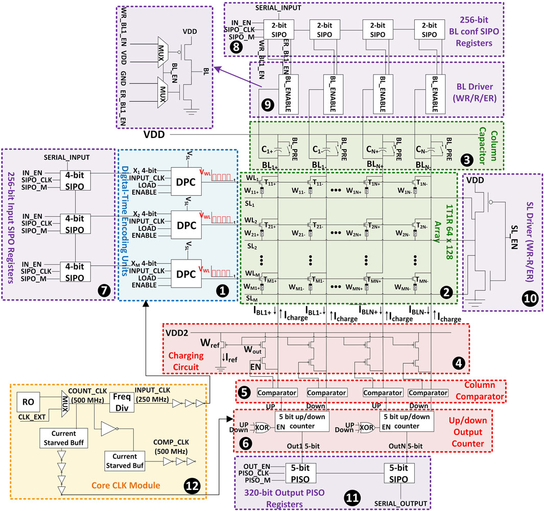
Figure 1. SPIKA macro architecture showing the input circuit (blue dashed rectangle), 1T1R array (green dashed rectangle, output circuit (red dashed rectangle), clock module (yellow dashed rectangle) and I/O interface and driving (purple dashed rectangle).
2.1 Input circuit
Here, row-wise digital-pulse-converter (DPC) units (label 1, Figure 1) convert incoming 4-bit digital inputs to a corresponding number of regularly-spaced voltage pulses at fixed-level
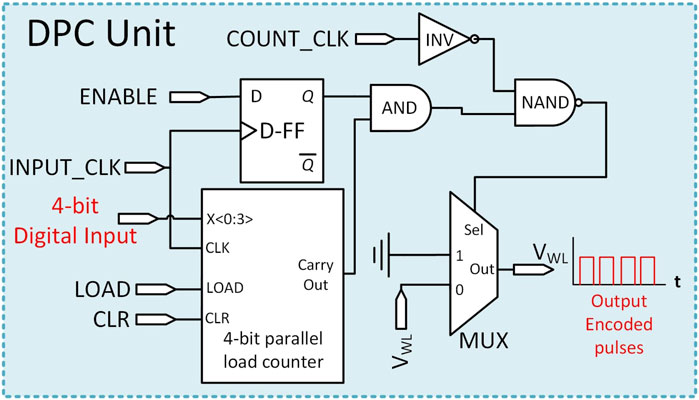
Figure 2. Digital-pulse-converter (DPC) circuit schematic.
2.2 1T1R array and column capacitors
The weights of the NN are mapped as resistances in the RRAM cells. In SPIKA, we use a ternary encoding scheme for the weights where positive and negative weights are stored in adjacent columns. The high resistive state (HRS) represents weight 0 and the low resistive state (LRS) represents weight 1 on positive columns and −1 on negative columns. Note that while the weight range is ternary, the RRAM devices are only required to be able to assume 2
A modified structure of the conventional 1T1R crossbar (Humood et al., 2019) is configured in SPIKA (label 2, Figure 1), this allows the crossbar to act as a current sink to the column capacitors (label 3, Figure 1). WLs are shared across the row and connect to the gate terminal of the access transistor in the 1T1R cell. Source-lines (SLs) are connected to a driver that determines the memristor (MR) mode of operation (writing/reading/erasing). Bit-lines (BLs) are shared across the columns and connect the column capacitors with the drain of the access transistors and the output circuits. Table 1 provides a summary of the array mode of operation in relation to the WL/BL and SL voltages. In addition, the table includes the voltage across the RRAM device in each mode and the peak current passing through the device.
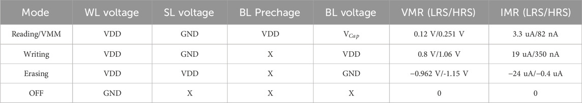
Table 1. RRAM mode of operations with relation to the WL/SL/BL voltages. X denotes do not care.
2.3 Output circuit
2.3.1 Charging circuit
The charging circuit in SPIKA (label 4, Figure 1) is used to charge the column capacitors
2.3.2 Comparator
A low-power double-tail dynamic comparator presented by Babayan-Mashhadi and Lotfi (2014) is designed in SPIKA (label 5, Figure 1). The comparator schematic is shown in Figure 3A. The sizing of the comparator was optimized for area, power, offset and decision time. Figure 3B summarizes the comparator performance generated by post-layout and Monte-Carlo simulations. The comparator in SPIKA tracks the BL voltage and issues requests for clicking once the capacitor voltage falls below the threshold value.
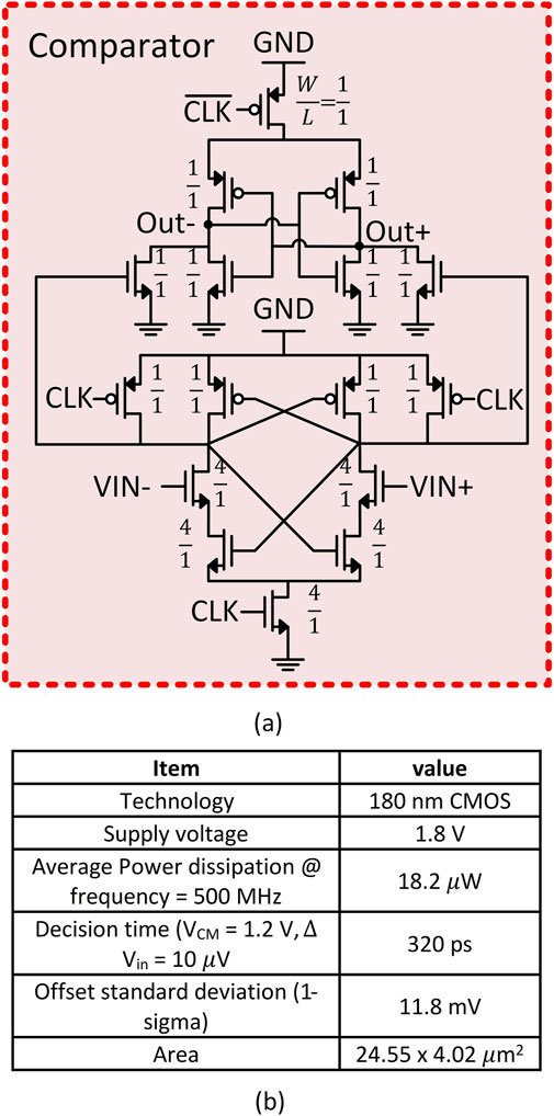
Figure 3. (a) SPIKA double tail dynamic comparator schematic, the ratios on the transistors
2.3.3 5-Bit UP/DOWN counter
The output analog to digital conversion in SPIKA is realized through synchronous 5-bit UP/DOWN counters (label 6, Figure 1) without the need for power-hungry ADCs as a result of the novel clicking mechanism implemented in this work. Every 2 adjacent columns in the array share one counter, when a column requests a click, the counter value is incremented or decremented whether it is the positive weight column or the negative weight column that issued the click. If both columns issue a click at the same cycle, the counter remains at its value which is implemented by clock gating. The final output of the counter is a signed 5-bit digital value.
2.4 I/O interface, registers and drivers
SPIKA is a fully integrated macro and includes several registers, drivers and control units for I/O communication and configurations as shown in Figure 1 (purple color rectangle box). There are 4 I/O units used in SPIKA. First, from the input circuit, a 256-bit serial in parallel out (SIPO) register (label 7, Figure 1) is designed to stream the digital inputs of the neural network to the input circuit units. Besides, the input registers can also be used to activate selected WLs for writing or erasing operations of the RRAM cell. Second, the BL configuration SIPO registers and BL driver units (label 8 and label 9, Figure 1) are used to configure the selected BLs of the 1T1R crossbar for writing/reading or erasing operations. Third, the SL driver unit (label 10, Figure 1) is used to configure the SLs of the 1T1R crossbar to either writing/reading or erasing modes. Finally, a 320-bit parallel in serial out (PISO) register (label 11, Figure 1) is used to stream out the outputs of the column counters.
2.5 SPIKA clock module
In SPIKA, the clock distribution can be divided into two sections: first, an external clock supply for the I/O interface and serial registers which runs at a lower frequency (e.g., 10 MHz) as the control configuration signals are loaded once during the setup time. The other clock module (core clock module) is generated internally and it supplies the core computation elements (label 12, Figure 1). The core clock module is shown in Figure 4 and can be divided into three parts. The first part is defined as CLK Generation where three clock signals are generated from a single ring oscillator (RO) that feeds different blocks in the core. The RO is powered by an external DC current source

Figure 4. SPIKA core clock generation and distribution module.
3 Operation and design methodology
3.1 VMM process and clicking mechanism
The VMM process is the main operation mode in NNs. In order to achieve a highly efficient system, it is important to perform low-power and low-latency VMM operations. Figure 5 presents a simplified view of SPIKA architecture highlighting the VMM process by showing the necessary blocks to compute one 5-bit output
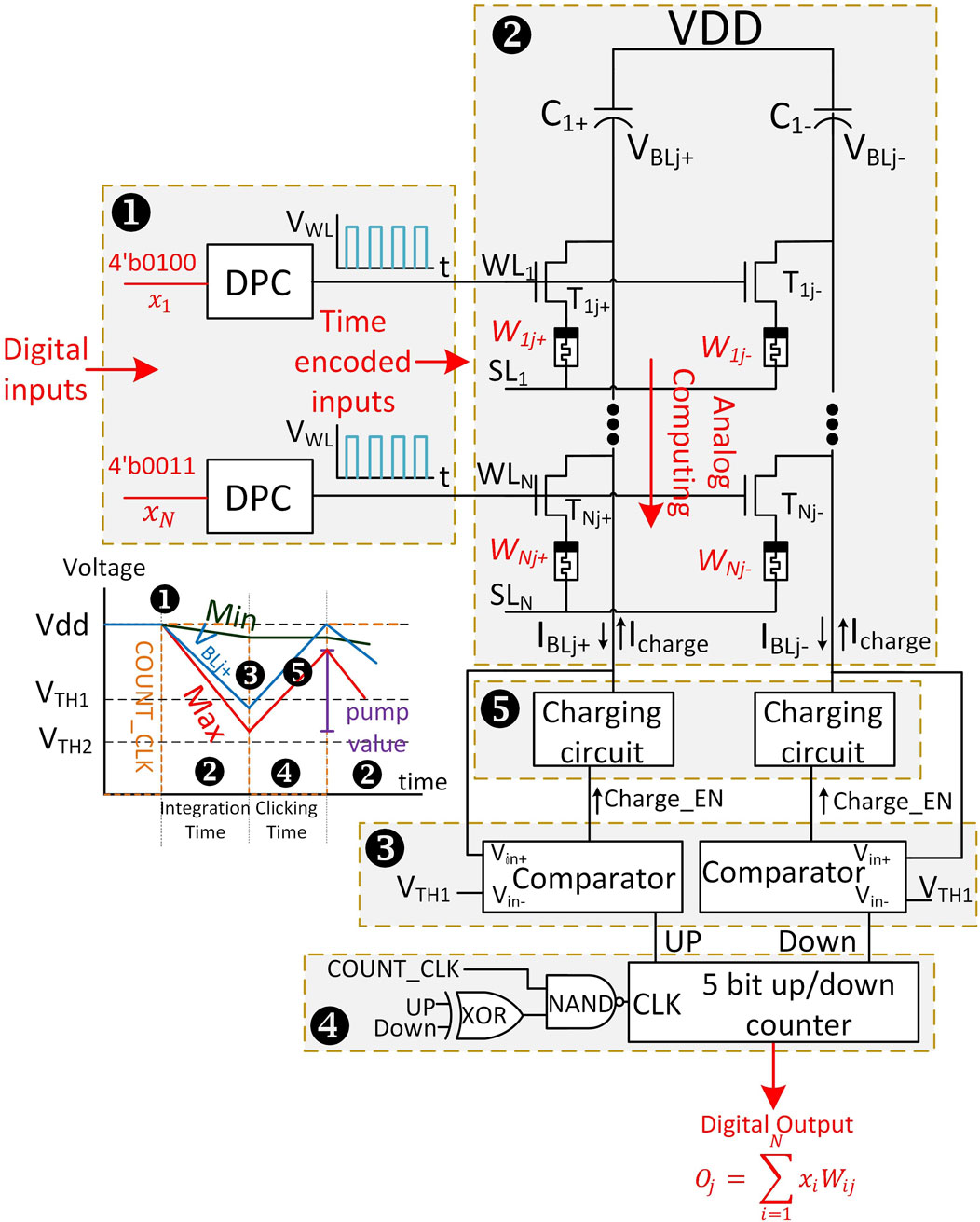
Figure 5. SPIKA simplified circuit schematic highlighting the VMM process and clicking mechanism.
In SPIKA, the VMM process is realized through a memory read operation. Once the inputs are loaded, the VMM operation is enabled where the digital inputs are modulated as discrete pulses through the DPC blocks. Then, the capacitor starts discharging through the activated 1T1R rows across the same column (integration time). The discharge rate of the capacitor is directly related to the combination of the inputs and weights where stronger inputs (higher number of pulses) and stronger weights (lower column resistance) lead to a higher discharge rate. When the BL voltage
The timing diagram in Figure 5 shows the discharge rate of column j
In SPIKA, every two adjacent columns share one counter. While one column stores positive weights and increments the counter, the other column stores the negative weights and decrements the counter once it requests a click. Hence, there is no need for additional subtractor units to implement the negative weights. The latency of one VMM operation in SPIKA is 60 ns and it is divided equally between integration time (active time) and clicking time (inactive time).
3.2 SPIKA constraints and design parameters
The key design objective in the VMM process is to ensure that the discharge rate of each column capacitor can be assumed linear, leading to linearly map the matrix product: Output = Inputs
3.2.1 WL voltage and RRAM read voltage
The WL voltage
3.2.2 Capacitor-discharge operation and
The discharge rate of the switched-based capacitor in this work controls the number of total clicks where higher discharge rates lead to a higher number of clicks. During integration time, the BL voltage of output
where
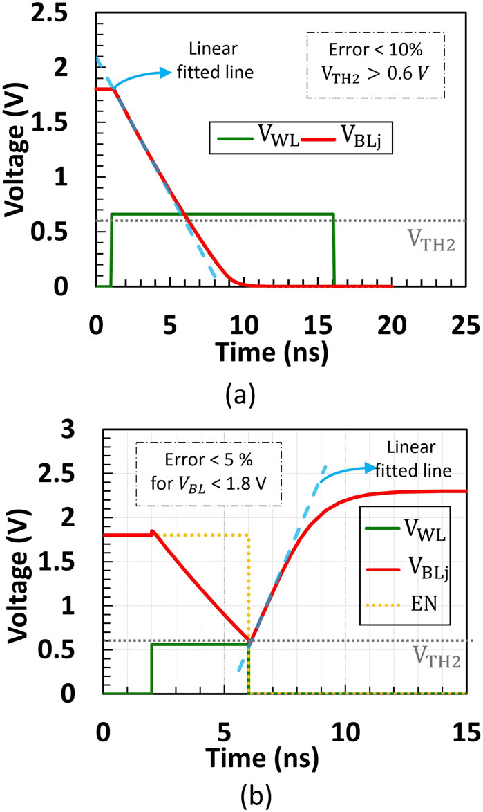
Figure 6. Transient simulation of the BL voltage
3.2.3 Capacitor charge operation
The current mirror shown in Figure 1 is responsible for charging the capacitor after a click. An external DC current reference is fed to the current mirror to provide appropriate current to the columns of the 1T1R array. Hence, the charging rate can be controlled even post-chip fabrication. Similar to the discharge operation, the design parameters of the current mirror must be precisely designed to ensure that the charging rate of the capacitor is linearly approximated. By ensuring this, the capacitor will be charged with the same amount of charge regardless of the voltage it clicked at. Since the BL pre-charged is at 1.8 V, linearity needs to be presumed up to 1.8 V. This is implemented by powering the current mirror at a voltage higher than 1.8 V. In SPIKA, the minimum power supply required to maintain linearity (with a maximum error percentage
3.2.4 Input boundary cases and system balance
In order to balance the system and the number of clicks, three boundary cases highlighted in Figure 7 need to be considered. The first case is denoted as Max input Max weight case (Case 1, Figure 7). In SPIKA each output is a 5-bit signed output which means that the maximum number of clicks a column can request is 15 clicks. In addition, since the number of rows is 64, the maximum number of active rows (N) is 64. The maximum row active time (30 ns) is achieved when the digital input is maximum, i.e. 4′b1111. The second case is denoted as Min input Min weight or Min input Max weight (Case 2, Figure 7). In this case, the inputs are 0 (N = 0), thus, the column capacitor will not discharge through the 1T1R cells regardless of the values of the weights. The third case is denoted as Max input Min weight case (Case 3, Figure 7). In this case, all inputs are activated (N = 64) for the maximum active time (
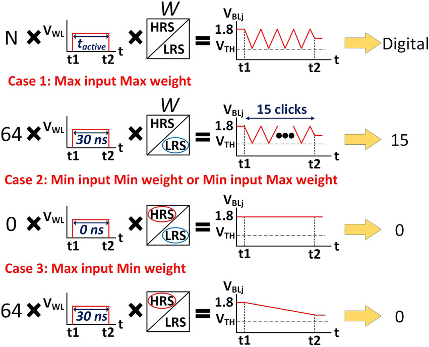
Figure 7. Input boundary cases of the clicking process.
Thus, with the discharging and the charging rates linearity assumed earlier, balancing the system around the boundary cases leads to a linear mapping of the in-between cases. In SPIKA, the discharge rate is balanced by the external voltage supply
3.2.5 Upper clicking threshold voltage
3.2.6 SPIKA resolution and scalability
The choice of using 4-bit input/5-bit output resolutions in SPIKA is driven by the need to maximize power efficiency while maintaining acceptable classification accuracy. The 4-bit input resolution represents an optimal balance for the time-encoding scheme. The selection is driven by the well-known challenge of linear time encoding, where increasing from 4-bit to 5-bit encoding doubles the maximum time required (Serb and Prodromakis, 2019). We note that time-domain encoding tends to be most competitive in the 2-4-bit range. The use of ternary weight representation is based on the fact that RRAM devices only need to support two states, a relaxed requirement that broadens compatibility with various RRAM technologies being developed worldwide. Research has shown that ternary representation works well for most CNN classifiers (Yang et al., 2023). However, future work will explore multi-bit RRAM devices to enhance scalability further. To scale the system for larger networks, the approach could involve splitting high-resolution inputs, weights, and outputs into multiple adjacent ones rather than increasing the resolution. For example, an 8-bit input can be divided across two rows, a method that has been successful in system-level nvCIM designs like ISAAC (Shafiee et al., 2016) and PRIME (Chi et al., 2016).
4 Results
In this work, SPIKA macro has been validated in Cadence circuit tools by performing simulations and analysis on extracted post-layout views, including resistance and capacitance parasitics using a commercial 180 nm process and experimental RRAM models (Maheshwari et al., 2021a; Maheshwari et al., 2021b).
4.1 Transient simulation of input boundary cases
Figure 8 presents the SPICE post-layout simulation of SPIKA under the Max input Max weight case (Case 1, Figure 7) and Max input Min weight case (Case 3, Figure 7) showing the output result for two columns (
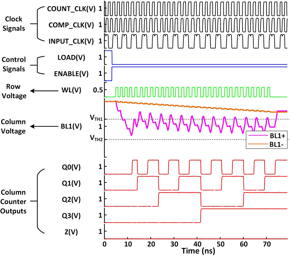
Figure 8. SPICE post-layout simulation of SPIKA for the Max input Max weight case (BL1+) and the Max input Min weight case (BL1-).
4.2 CMOS process corner analysis
Table 2 provides a summary of the SPIKA process corner analysis conducted at 27 °C across five different CMOS process corners (nmos-pmos). The analysis is simulated under four distinct input (IN)/weight (W) combinations, where a higher percentage signifies stronger inputs and weights. For example, in case 1 (100% IN 100% W) all inputs are activated for the maximum duration and all weights are in the LRS. As we recall from Section 3.2.4, this case corresponds to the boundary case of the maximum input and maximum weight (15 clicks at the output). Table 2 shows the least significant bit (LSB) deviation between the simulated output and expected output for each corner and case. A deviation of 0 LSB indicates a correct conversion, highlighted in green in the table. Red-highlighted cells indicate incorrect conversions, along with the extent to which the simulated output deviates from the expected output.
Table 2. SPIKA process corner analysis conducted at 27°C for different input (IN)/weight (W) combinations. The least significant bit (LSB) provides an indication of the deviation between the simulated output and the expected output.
The results anticipated in Table 2 are divided into two segments, before balancing and after balancing. Recall that balancing in SPIKA is controlled by two external sources,
Nevertheless, the inherent balancing mechanism in SPIKA, regulated by independent external sources, allows for the adjustment of the discharging rate to accommodate different corners. Parametric simulations demonstrated that adjusting only
4.3 Temperature variation analysis
Similar to the process corner analysis, the SPIKA core was simulated across a temperature range spanning from −55°C to 125 °C and typical process corner. The outcomes for various IN/W cases are summarized in Table 3. The table comprises two sections, similar to the process corner analysis: before balancing and after balancing segments. In the before-balancing segment, the results indicate that lower temperatures lead to a lower discharge rate, resulting in fewer clicks, while higher temperatures result in a higher discharge rate and more clicks. As demonstrated before, the SPIKA system can be adjusted to function in various temperature ranges by optimizing the
Table 3. SPIKA temperature variation analysis conducted at TT corner for different input (IN)/weight (W) combinations. The least significant bit (LSB) provides an indication of the deviation between the simulated output and the expected output.
4.4 Monte Carlo analysis
SPIKA core have been simulated using Monte Carlo analysis to investigate the impact of CMOS mismatch. Figures 9A–D presents the histogram results for four distinct input (IN)/weight (W) combinations. The LSB represents the difference between the simulated output and the expected output, with 0 LSB indicating a correct conversion. As depicted in Figure 9, the lowest success rate is seen in case 1 (Figure 9A) with a 98.5% success rate. This outcome aligns with expectations, as more active input/weight combinations involve a higher number of active 1T1R cells, introducing more transistor mismatch effect. Conversely, the success rate is found to be 100% in cases 3 and 4, where the number of activated input/weight cells is lower.
Figure 9. (a–d) Histogram of Monte Carlo process mismatch simulated at the TT Corner and room temperature for four distinct input/weight combinations. The correct output is represented by 0 LSB.
4.5 RRAM variation analysis
As mentioned previously in Section 2.2, we implement a ternary weight encoding scheme in SPIKA, where the RRAM devices are only required to support a total of 2
However, Table 4 demonstrates that even in the absence of a successful write-verify mechanism, the SPIKA system remains robust against variations in both LRS and HRS values. In this analysis, RRAM LRS and HRS resistances were swept from −20% to +20%, and any deviation from the correct conversion accuracy was quantified in terms of LSB error. It is important to highlight that these simulations represent a worst-case scenario, where all RRAM devices in the array are subjected to identical variation. The results indicate that noticeable conversion deviation only begins when LRS variations exceed 15%, with the maximum error observed being 2 LSBs at a 20% variation. These findings suggest that such high levels of variation—15%–20% across all RRAM devices simultaneously—represent an extremely unlikely worst-case scenario, and the resulting deviations remain minimal, further highlighting the robustness of the SPIKA system to device-level variability.
Table 4. SPIKA RRAM variation analysis conducted at 27°C. The least significant bit (LSB) provides an indication of the deviation between the simulated output and the expected output. The low resistive state (LRS) is set to 40 k
4.6 Power and area breakdown
Table 5 presents the average power consumption and area breakdown of each component in SPIKA including the I/O and control circuitry. The metrics in Table 5 are based on post-layout extracted simulations and views and a randomized set of inputs and weights. The power and area overhead of the input and output circuits in SPIKA are 57% and 26%, respectively, which is an improvement of 22% and 6% of the power and area overhead of the ISAAC structure (Shafiee et al., 2016) running at 32 nm CMOS technology. The computational core consumes an average of
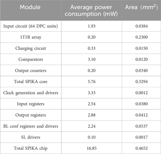
Table 5. SPIKA macro area and power breakdown.
5 Circuit-level metrics and benchmarking
5.1 SPIKA energy efficiency and throughput and comparison with baseline nv-CIM
The energy per operation for a given task is a key metric to benchmark hardware accelerators (Seo et al., 2022). The computational blocks in SPIKA consume an average power of 5.6 mW during a single VMM process, with an array size of
To benchmark SPIKA against the baseline nv-CIM, we refer to the ISAAC core reported by Shafiee et al., which utilizes DACs for input encoding and ADCs for output conversion, performing multiplications in the current domain (Shafiee et al., 2016). The ISAAC core consumes average power of 27.5 mW during a single VMM process with a
5.2 Comparison with state of the art
Table 6 provides a performance summary of SPIKA CIM macro compared to prior works. The throughput and energy efficiency are determined for the computing cells only so that system-level related effects are not taken into account. Where reported values were system-level, they were recalculated specifically for CIM macros. Compared with the core proposed by Cai running at a similar technology node (180 nm) and array size (Cai et al., 2019), SPIKA provides a 12
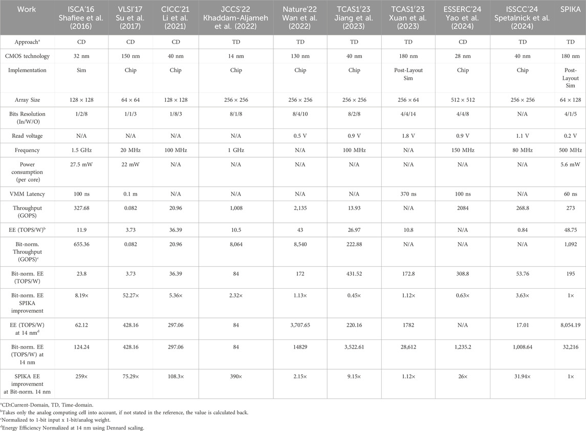
Table 6. Comparison table with state-Of-The-Art CIM macro designs. norm.: Bit-Normalized. EE, Energy efficiency.
The SPIKA CIM macro, implemented with a 180 nm technology node, demonstrates an energy efficiency of 48.75 TOPS/W (for 4b input x 1b weight), which is comparable to state-of-the-art implementations at advanced technology nodes. To provide further perspective we also show bit-normalised throughput and energy efficiency. The SPIKA core ranks highest in raw energy efficiency in the table and third-highest in bit-normalized energy efficiency (Jiang et al., 2023). and (Yao et al., 2024) topped the bit-normalized energy efficiency. We attribute this to a combination of using a more advanced technology node and including no output circuits, where the outputs of the CIM macro remain in analog form and are not converted to digital until later at the system level.
For further perspective, we also projected the energy efficiency of all designs to 14 nm using Dennard scaling assumptions (normalization factor of
5.3 Chip summary
Figure 10 presents a post-layout capture of SPIKA chip (I/O pads included) along with a specification summary. Our system performance could be further improved by using more advanced technology nodes and optimizing the computing architecture and peripheral circuits. For example, the column capacitors could be integrated beneath the RRAM array if additional metal layers are available, this could save up to 4% of the total area from savings in the core alone. In addition, having more metal layers could decrease the pitch size of the 1T1R cell and the peripheral circuits leading to a denser structure.
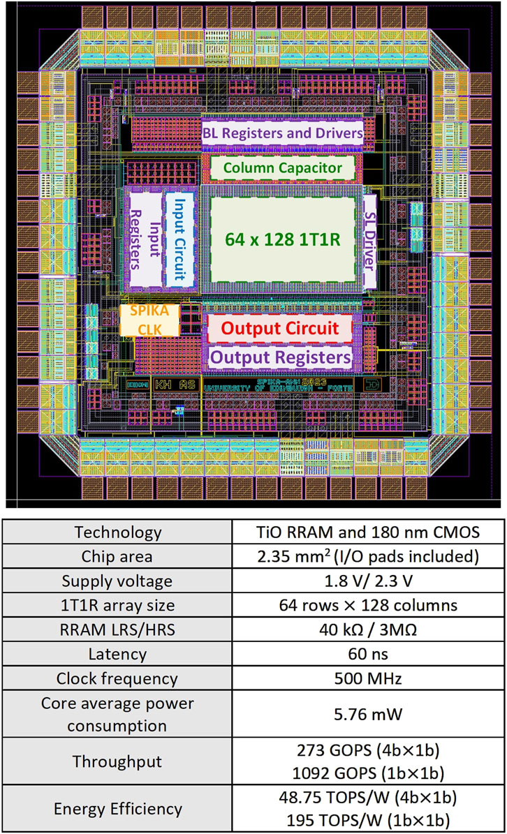
Figure 10. SPIKA Post-layout chip capture and specification summary.
6 Conclusion and future work
This work proposed a novel time-domain RRAM-based non-volatile compute-in-memory (nvCIM)
The characterization results obtained in this work highlight the potential of nvCIM macros in AI edge computation. The SPIKA core, as designed here, is optimized for vector matrix multiplication (VMM) operations, a critical function across various neural network classifiers, including deep neural networks (DNNs), convolutional neural networks (CNNs), and spiking neural networks (SNNs). The decision to utilize 4-bit inputs, 5-bit inputs, and ternary weights is aimed at maximizing power efficiency while ensuring satisfactory classification accuracy. Similar configurations have demonstrated impressive classification performance, as demonstrated by Yang et al. (2023) and Zhang et al. (2024). Future work will focus on developing a multi-core system-level design for SPIKA, enabling the efficient implementation of comprehensive workloads.
Data availability statement
The original contributions presented in the study are included in the article/Supplementary Material, further inquiries can be directed to the corresponding author.
Author contributions
KH: Conceptualization, Methodology, Software, Validation, Visualization, Writing – original draft, Writing – review and editing. YP: Software, Visualization, Writing – review and editing. GR: Software, Validation, Writing – review and editing. MM: Software, Writing – review and editing. SW: Supervision, Writing – review and editing. AS: Investigation, Methodology, Supervision, Writing – review and editing. TP: Funding acquisition, Supervision, Writing – review and editing.
Funding
The author(s) declare that financial support was received for the research and/or publication of this article. This work was supported by the Engineering and Physical Sciences Research Council (EPSRC) Programme Grant EP/R024642/2 “Functional Oxide Reconfigurable Technologies (FORTE)” and the RAEng Chair in Emerging Technologies (CiET 1819/2/93).
Acknowledgments
The authors would like to thank Shady Agwa and Sachin Maheshwari for their valuable discussion and support.
Conflict of interest
The authors declare that the research was conducted in the absence of any commercial or financial relationships that could be construed as a potential conflict of interest.
Generative AI statement
The author(s) declare that no Generative AI was used in the creation of this manuscript.
Publisher’s note
All claims expressed in this article are solely those of the authors and do not necessarily represent those of their affiliated organizations, or those of the publisher, the editors and the reviewers. Any product that may be evaluated in this article, or claim that may be made by its manufacturer, is not guaranteed or endorsed by the publisher.
Supplementary material
The Supplementary Material for this article can be found online at: https://www.frontiersin.org/articles/10.3389/felec.2025.1567562/full#supplementary-material
References
Alemdar, H., Leroy, V., Prost-Boucle, A., and Pétrot, F. (2017). “Ternary neural networks for resource-efficient ai applications,” in 2017 International Joint Conference on Neural Networks (IJCNN), USA, 14-19 May 2017, 2547–2554. doi:10.1109/ijcnn.2017.7966166
Amirsoleimani, A., Alibart, F., Yon, V., Xu, J., Pazhouhandeh, M. R., Ecoffey, S., et al. (2020). In-memory vector-matrix multiplication in monolithic complementary metal–oxide–semiconductor-memristor integrated circuits: design choices, challenges, and perspectives. Adv. Intell. Syst. 2, 2000115. doi:10.1002/aisy.202000115
Ankit, A., Sengupta, A., Panda, P., and Roy, K. (2017). Resparc: a reconfigurable and energy-efficient architecture with memristive crossbars for deep spiking neural networks, 1, 6. doi:10.1145/3061639.3062311
Babayan-Mashhadi, S., and Lotfi, R. (2014). Analysis and design of a low-voltage low-power double-tail comparator. IEEE Trans. Very Large Scale Integration (VLSI) Syst. 22, 343–352. doi:10.1109/TVLSI.2013.2241799
Bahdanau, D., Cho, K., and Bengio, Y. (2015). Neural machine translation by jointly learning to align and translate
Bayat, F. M., Prezioso, M., Chakrabarti, B., Nili, H., Kataeva, I., and Strukov, D. (2018). Implementation of multilayer perceptron network with highly uniform passive memristive crossbar circuits. Nat. Commun. 9, 2331. doi:10.1038/s41467-018-04482-4
Cai, F., Correll, J. M., Lee, S. H., Lim, Y., Bothra, V., Zhang, Z., et al. (2019). A fully integrated reprogrammable memristor–cmos system for efficient multiply–accumulate operations. Nat. Electron. 2, 290–299. doi:10.1038/s41928-019-0270-x
Chen, W.-H., Dou, C., Li, K.-X., Lin, W.-Y., Li, P.-Y., Huang, J.-H., et al. (2019). Cmos-integrated memristive non-volatile computing-in-memory for ai edge processors. Nat. Electron. 2, 420–428. doi:10.1038/s41928-019-0288-0
Chi, P., Li, S., Xu, C., Zhang, T., Zhao, J., Liu, Y., et al. (2016). “Prime: a novel processing-in-memory architecture for neural network computation in reram-based main memory,” in 2016 ACM/IEEE 43rd annual international symposium on computer architecture (ISCA), 27–39. doi:10.1109/ISCA.2016.13
Dennard, R., Gaensslen, F., Yu, H.-N., Rideout, V., Bassous, E., and LeBlanc, A. (1974). Design of ion-implanted mosfet’s with very small physical dimensions. IEEE J. Solid-State Circuits 9, 256–268. doi:10.1109/JSSC.1974.1050511
Graves, A., Mohamed, A.-r., and Hinton, G. (2013). Speech recognition with deep recurrent neural networks, 6645, 6649. doi:10.1109/icassp.2013.6638947
Hertel, L., Barth, E., Käster, T., and Martinetz, T. (2015). “Deep convolutional neural networks as generic feature extractors,” in 2015 International Joint Conference on Neural Networks (IJCNN), USA, 12-17 July 2015, 1–4. doi:10.1109/ijcnn.2015.7280683
Humood, K., Hadi, S. A., Mohammad, B., Jaoude, M. A., Alazzam, A., and Alhawari, M. (2019). “High-density reram crossbar with selector device for sneak path reduction,” in 2019 31st International Conference on Microelectronics (ICM), USA, 15-18 December 2019, 244–248. doi:10.1109/ICM48031.2019.9021944
Humood, K., Pan, Y., Wang, S., Serb, A., and Prodromakis, T. (2024). Design of a low-power digital-to-pulse converter (dpc) for in-memory-computing applications. Microelectron. J. 153, 106420. doi:10.1016/j.mejo.2024.106420
Humood, K., Serb, A., Wang, S., and Prodromakis, T. (2023a). “Power, performance and area optimization of parallel load counters through logic minimization and tspc-ff utilization,” in 2023 30th IEEE International Conference on Electronics, Circuits and Systems (ICECS), USA, 04-07 December 2023, 1–5. doi:10.1109/ICECS58634.2023.10382888
Humood, K., Serb, A., Wang, S., and Prodromakis, T. (2023b). “Quicknn: Python toolbox for training and optimizing ann for hardware implementation,” in 2023 IEEE 66th international midwest symposium on circuits and systems (MWSCAS), 531–535. doi:10.1109/MWSCAS57524.2023.10405963
Hung, J.-M., Xue, C.-X., Kao, H.-Y., Huang, Y.-H., Chang, F.-C., Huang, S.-P., et al. (2021). A four-megabit compute-in-memory macro with eight-bit precision based on cmos and resistive random-access memory for ai edge devices. Nat. Electron. 4, 921–930. doi:10.1038/s41928-021-00676-9
Jiang, H., Huang, S., Li, W., and Yu, S. (2023). Enna: an efficient neural network accelerator design based on adc-free compute-in-memory subarrays. IEEE Trans. Circuits Syst. I Regul. Pap. 70, 353–363. doi:10.1109/TCSI.2022.3208755
Ji-Ren, Y., Karlsson, I., and Svensson, C. (1987). A true single-phase-clock dynamic cmos circuit technique. IEEE J. Solid-State Circuits 22, 899–901. doi:10.1109/JSSC.1987.1052831
Kadetotad, D., Xu, Z., Mohanty, A., Chen, P. Y., Lin, B., Ye, J., et al. (2015). Parallel architecture with resistive crosspoint array for dictionary learning acceleration. IEEE J. Emerg. Sel. Top. Circuits Syst. 5, 194–204. doi:10.1109/JETCAS.2015.2426495
Khaddam-Aljameh, R., Stanisavljevic, M., Fornt Mas, J., Karunaratne, G., Brändli, M., Liu, F., et al. (2022). Hermes-core—a 1.59-tops/mm2 pcm on 14-nm cmos in-memory compute core using 300-ps/lsb linearized cco-based adcs. IEEE J. Solid-State Circuits 57, 1027–1038. doi:10.1109/JSSC.2022.3140414
Li, B., Lixue, X., Peng, G., Wang, Y., and Huazhong, Y. (2015). “Merging the interface: power, area and accuracy co-optimization for rram crossbar-based mixed-signal computing system,” in 2015 52nd ACM/EDAC/IEEE design automation conference (DAC), 1–6. doi:10.1145/2744769.2744870
Li, W., Huang, S., Sun, X., Jiang, H., and Yu, S. (2021). “Secure-rram: a 40nm 16kb compute-in-memory macro with reconfigurability, sparsity control, and embedded security,” in 2021 IEEE Custom Integrated Circuits Conference (CICC), USA, 25-30 April 2021, 1–2. doi:10.1109/CICC51472.2021.9431558
Liu, Q., Gao, B., Yao, P., Wu, D., Chen, J., Pang, Y., et al. (2020). “33.2 a fully integrated analog reram based 78.4tops/w compute-in-memory chip with fully parallel mac computing,” in 2020 IEEE International Solid- State Circuits Conference - (ISSCC), USA, 16-20 February 2020, 500–502. doi:10.1109/ISSCC19947.2020.9062953
Maheshwari, S., Stathopoulos, S., Wang, J., Serb, A., Pan, Y., Mifsud, A., et al. (2021a). Design flow for hybrid cmos/memristor systems—part i: modeling and verification steps. IEEE Trans. Circuits Syst. I Regul. Pap. 68, 4862–4875. doi:10.1109/TCSI.2021.3122343
Maheshwari, S., Stathopoulos, S., Wang, J., Serb, A., Pan, Y., Mifsud, A., et al. (2021b). Design flow for hybrid cmos/memristor systems—part ii: circuit schematics and layout. IEEE Trans. Circuits Syst. I Regul. Pap. 68, 4876–4888. doi:10.1109/TCSI.2021.3122381
Marinella, M. J., Agarwal, S., Hsia, A., Richter, I., Jacobs-Gedrim, R., Niroula, J., et al. (2018). Multiscale co-design analysis of energy, latency, area, and accuracy of a reram analog neural training accelerator. IEEE J. Emerg. Sel. Top. Circuits Syst. 8, 86–101. doi:10.1109/jetcas.2018.2796379
Ming, C., Lixue, X., Zhenhua, Z., Yi, C., Yuan, X., Yu, W., et al. (2017). “Time: a training-in-memory architecture for memristor-based deep neural networks,” in 2017 54th ACM/EDAC/IEEE design automation conference (DAC), 1–6. doi:10.1145/3061639.3062326
Mittal, S. (2019). A survey of reram-based architectures for processing-in-memory and neural networks. Mach. Learn. Knowl. Extr. 1, 75–114. doi:10.3390/make1010005
Mochida, R., Kouno, K., Hayata, Y., Nakayama, M., Ono, T., Suwa, H., et al. (2018). “A 4m synapses integrated analog reram based 66.5 tops/w neural-network processor with cell current controlled writing and flexible network architecture,” in 2018 IEEE symposium on VLSI technology, 175–176.
Musisi-Nkambwe, M., Afshari, S., Barnaby, H., Kozicki, M., and Sanchez Esqueda, I. (2021). The viability of analog-based accelerators for neuromorphic computing: a survey. Neuromorphic Comput. Eng. 1, 012001. doi:10.1088/2634-4386/ac0242
Narayanan, S., Shafiee, A., and Balasubramonian, R. (2017). “Inxs: bridging the throughput and energy gap for spiking neural networks,” in 2017 International Joint Conference on Neural Networks (IJCNN), China, 14-19 May 2017, 2451–2459. doi:10.1109/IJCNN.2017.7966154
Prezioso, M., Mahmoodi, M. R., Bayat, F. M., Nili, H., Kim, H., Vincent, A., et al. (2018). Spike-timing-dependent plasticity learning of coincidence detection with passively integrated memristive circuits. Nat. Commun. 9, 5311. doi:10.1038/s41467-018-07757-y
Sahay, S., Bavandpour, M., Mahmoodi, M. R., and Strukov, D. (2020). Energy-efficient moderate precision time-domain mixed-signal vector-by-matrix multiplier exploiting 1t-1r arrays. IEEE J. Explor. Solid-State Comput. Devices Circuits 6, 18–26. doi:10.1109/JXCDC.2020.2981048
Sebastian, A., Le Gallo, M., Khaddam-Aljameh, R., and Eleftheriou, E. (2020). Memory devices and applications for in-memory computing. Nat. Nanotechnol. 15, 529–544. doi:10.1038/s41565-020-0655-z
Seo, J. S., Saikia, J., Meng, J., He, W., Suh, H. S., Anupreetham, H., et al. (2022). Digital versus analog artificial intelligence accelerators: advances, trends, and emerging designs. IEEE Solid-State Circuits Mag. 14, 65–79. doi:10.1109/MSSC.2022.3182935
Serb, A., and Prodromakis, T. (2019). “An analogue-domain, switch-capacitor-based arithmetic-logic unit,” in 2019 IEEE international symposium on circuits and systems (ISCAS), 1–5. doi:10.1109/ISCAS.2019.8702070
Shafiee, A., Nag, A., Muralimanohar, N., Balasubramonian, R., Strachan, J. P., Hu, M., et al. (2016). “Isaac: a convolutional neural network accelerator with in-situ analog arithmetic in crossbars,” in 2016 ACM/IEEE 43rd annual international symposium on computer architecture (ISCA), 14–26. doi:10.1109/ISCA.2016.12
Shim, W., sun Seo, J., and Yu, S. (2020). Two-step write–verify scheme and impact of the read noise in multilevel rram-based inference engine. Semicond. Sci. Technol. 35, 115026. doi:10.1088/1361-6641/abb842
Spetalnick, S. D., Lele, A. S., Crafton, B., Chang, M., Ryu, S., Yoon, J.-H., et al. (2024). 30.1 a 40nm vliw edge accelerator with 5mb of 0.256pj/b rram and a localization solver for bristle robot surveillance. 2024 IEEE Int. Solid-State Circuits Conf. (ISSCC) 67, 482–484. doi:10.1109/ISSCC49657.2024.10454500
Su, F., Chen, W. H., Xia, L., Lo, C. P., Tang, T., Wang, Z., et al. (2017). “A 462gops/j rram-based nonvolatile intelligent processor for energy harvesting ioe system featuring nonvolatile logics and processing-in-memory,” in 2017 symposium on VLSI technology, T260–T261. doi:10.23919/VLSIT.2017.7998149
Tang, S., Yin, S., Zheng, S., Ouyang, P., Tu, F., Yao, L., et al. (2017). “Aepe: an area and power efficient rram crossbar-based accelerator for deep cnns,” in 2017 IEEE 6th non-volatile memory systems and applications symposium (NVMSA), 1–6. doi:10.1109/NVMSA.2017.8064475
Wan, W., Kubendran, R., Schaefer, C., Eryilmaz, S. B., Zhang, W., Wu, D., et al. (2022). A compute-in-memory chip based on resistive random-access memory. Nature 608, 504–512. doi:10.1038/s41586-022-04992-8
Wang, Y., Tang, T., Xia, L., Li, B., Gu, P., Yang, H., et al. (2015). Energy efficient rram spiking neural network for real time classification. GLSVLSI '15: Proceedings of the 25th edition on Great Lakes Symposium on VLSI, 189, 194. doi:10.1145/2742060.2743756
Xia, L., Tang, T., Huangfu, W., Cheng, M., Yin, X., Li, B., et al. (2016). “Switched by input: power efficient structure for rram-based convolutional neural network,” in 2016 53nd ACM/EDAC/IEEE Design Automation Conference (DAC), USA, 4 Nov 2022, 1–6. doi:10.1145/2897937.2898101
Xuan, Z., Liu, C., Zhang, Y., Li, Y., and Kang, Y. (2023). A brain-inspired adc-free sram-based in-memory computing macro with high-precision mac for ai application. IEEE Trans. Circuits Syst. II Express Briefs 70, 1276–1280. doi:10.1109/TCSII.2022.3224049
Xue, C., Huang, T., Liu, J., Chang, T., Kao, H., Wang, J., et al. (2020). “15.4 a 22nm 2mb reram compute-in-memory macro with 121-28tops/w for multibit mac computing for tiny ai edge devices,” in 2020 IEEE International Solid-State Circuits Conference - (ISSCC), USA, 16-20 February 2020, 244–246. doi:10.1109/ISSCC19947.2020.9063078
Yang, X., Zhu, K., Tang, X., Wang, M., Zhan, M., Lu, N., et al. (2023). An in-memory-computing charge-domain ternary cnn classifier. IEEE J. Solid-State Circuits 58, 1450–1461. doi:10.1109/JSSC.2023.3238725
Yao, P., Wei, Q., Wu, D., Gao, B., Yang, S., Shen, T.-Y., et al. (2024). “A 28 nm rram-based 81.1 tops/mm2/bit compute-in-memory macro with uniform and linear 64 read channels under 512 4-bit inputs,” in 2024 IEEE European Solid-State Electronics Research Conference (ESSERC), Belgium, 09-12 September 2024, 577–580. doi:10.1109/ESSERC62670.2024.10719511
Yao, P., Wu, H., Gao, B., Tang, J., Zhang, Q., Zhang, W., et al. (2020). Fully hardware-implemented memristor convolutional neural network. Nature 577, 641–646. doi:10.1038/s41586-020-1942-4
Yu, S., Jiang, H., Huang, S., Peng, X., and Lu, A. (2021). Compute-in-memory chips for deep learning: recent trends and prospects. IEEE Circuits Syst. Mag. 21, 31–56. doi:10.1109/MCAS.2021.3092533
Yu, S., Li, Z., Chen, P. Y., Wu, H., Gao, B., Wang, D., et al. (2016). “Binary neural network with 16 mb rram macro chip for classification and online training,” in 2016 IEEE international electron devices meeting (IEDM). doi:10.1109/IEDM.2016.7838429
Zhang, B., Saikia, J., Meng, J., Wang, D., Kwon, S., Myung, S., et al. (2024). Macc-sram: a multistep accumulation capacitor-coupling in-memory computing sram macro for deep convolutional neural networks. IEEE J. Solid-State Circuits 59, 1938–1949. doi:10.1109/JSSC.2023.3332017
Keywords: in-memory-computing, RRAM, IMC, CIM, accelerators, VMM, analog-computing
Citation: Humood K, Pan Y, Reynolds G, Mughal M, Wang S, Serb A and Prodromakis T (2025) SPIKA: an energy-efficient time-domain hybrid CMOS-RRAM compute-in-memory macro. Front. Electron. 6:1567562. doi: 10.3389/felec.2025.1567562
Received: 27 January 2025; Accepted: 15 April 2025;
Published: 30 April 2025.
Edited by:
Sumeet Kumar Gupta, Purdue University, United StatesReviewed by:
Abhronil Sengupta, The Pennsylvania State University (PSU), United StatesJeffry Victor, Purdue University, United States
Copyright © 2025 Humood, Pan, Reynolds, Mughal, Wang, Serb and Prodromakis. This is an open-access article distributed under the terms of the Creative Commons Attribution License (CC BY). The use, distribution or reproduction in other forums is permitted, provided the original author(s) and the copyright owner(s) are credited and that the original publication in this journal is cited, in accordance with accepted academic practice. No use, distribution or reproduction is permitted which does not comply with these terms.
*Correspondence: Khaled Humood, Sy5NLk0uSHVtb29kQHNtcy5lZC5hYy51aw==