 Giovanni Bella1†
 Paolo Calorenni1
 Neeraj Yadav2*
 Emanuele Luigi Sciuto1*
 Angelo Alberto Messina3Katia Buonasera4†
 Leandro Lorenzelli2
 Sabrina Conoci1,5
- 1Department of Chemical, Biological, Pharmaceutical and Environmental Sciences, University of Messina, Messina, Italy
- 2Center for Sensors and Devices (SD), FBK—Foundation Bruno Kessler, Trento, Italy
- 3STMicroelectronics, Catania, Italy
- 4Consiglio Nazionale delle Ricerche (CNR), Institute for Microelectronics and Microsystems (IMM), Messina, Italy
- 5Department of Chemistry “Giacomo Ciamician”, University of Bologna, Bologna, Italy
The technological evolution towards portable systems for nucleic acids (NAs) analysis is central in diagnostics and healthcare. Conventional approaches for genetic analysis require multistep procedures, from the genetic material purification to its detection, that are mostly based on the NA amplification by polymerase chain reaction (PCR) and constrained to bulky specialized instruments and dedicated laboratories. These limitations imply an increase in time and cost of analysis avoiding the possibility of massive molecular screening, as in the case of an infectious pandemic, and accessible diagnosis. Therefore, research efforts are moving towards new Lab-on-a-chip (LoC) technologies that guarantee a more integrated, decentralized, user-friendly, and low-cost NA analysis. These are based on miniaturized optical or electrical chips on which it is possible to integrate a sensing surface for specific analytical applications. In this scenario, we presented the fabrication and characterization of a miniaturized electrochemical (EC) biochip as a potential LoC for genetic applications. The chip was developed with microfabricated electrodes on top and polycarbonate/PDMS microchambers for the surface treatment and functionalization. The characterization of chip EC performances has been performed by cyclic voltammetry (CV) and electrochemical impedance spectroscopy (EIS). Moreover, the chip surface has been functionalized with thiol-modified oligonucleotides, whose immobilization has been characterized by contact angle (CA) and surface free energy (SFE) analysis. Results reported a good robustness and responsivity of the chip proving its suitability for sensing array preparation and integration in a LoC format.
1 Introduction
The analysis of nucleic acids (NA) in molecular diagnostics is widely used in biomedical research and enables the study of entire genomes and transcriptomes, providing deeper insights into biological processes, disease mechanisms, and personalized medicine. However, NA analysis decentralization and accessibility are strictly limited by the implied analytical procedures and architecture (Sciuto et al., 2021). Indeed, consolidated techniques for molecular diagnostics such as Real-Time PCR (Schmittgen et al., 2008; Chen et al., 2011), next-generation sequencing (NGS) (Hu et al., 2017) and microarrays (Nelson et al., 2004; Lim et al., 2005), require multistep approaches where the target NA is first extracted and purified from a biological sample (blood, urine, saliva, etc.) with commercial kits, and detected. Moreover, the NA detection usually relies on the amplification by PCR reaction that, although extensively studied and optimized, implies a high time and cost consumption, due to the required thermal cycling and reagents, together with a lab constraint, due to the bulky instrumentation used and the need for specialized personnel.
The technologies for point-of-care (PoC) diagnostics overcome these limitations opening towards a new frontier of healthcare based on the decentralization of molecular analysis management and the speed up of therapeutic interventions. Recent progress in PoC diagnostics mostly concerns fully integrated systems prototypes and commercial products based on disposable cartridges (mainly made of plastic materials to reduce the cost of the analysis) integrating all the necessary reagents, microfluidic actuation, thermal and detection modules for the final analysis in a sample-in-answer-out format. However, PoC diagnostics still requires a technological improvement focusing on the optimization of material properties used (overcoming the plastics drawbacks), the down-scaling of systems architectures (droplets, nanobeads, etc.), the high-level electronics on-board integration and the reduction of system complexity (Petralia and Conoci, 2017). In this sense, the electrochemical sensing technologies attracted a lot of interest for molecular diagnostics due to their intrinsic rapidity and high sensitivity (Gao et al., 2019; Park et al., 2019; Pandey et al., 2022). The EC sensing offers performances that are suitable for a short-time analysis in a highly portable and miniaturized system, keeping a good level of accuracy. This is the case of the EC LoC systems (Pereira et al., 2023) that rely on the integration in a single miniaturized device of multiple laboratory processes, including NA extraction, mixing and detection, for many sensing applications, such as viral (Najjar et al., 2022) or bacterial detection (Srikanth et al., 2022) and clinical diagnosis (Zhu et al., 2019; Sierra et al., 2020; Borriello et al., 2023).
Herein, we developed a miniaturized EC biochip suitable for LoC genetic applications of NAs sensing. The system consisted of a microfabricated electrode on top that can be modified by grafting complementary thiolate oligonucleotides as probes for molecular sensing applications. The system EC properties were deeply characterized by CV and EIS analysis under different conditions, also estimating the active area of the electrode surface. In parallel, the assembly of a surface array, suitable for genetic sensing applications, was first validated by modifying the surface of the platinum working electrode in drop casting mode and testing the effectiveness of functionalization by CA analysis.
2 Materials and methods
2.1 Chemicals
Phosphate buffered saline (PBS) 0.01 M solution at pH 6.0, ultrapure water, 0.2 M phosphate buffer (Pb) at pH 6.8, potassium chloride (KCl) 0.1 M, sulfuric acid (H2SO4) 0.05 M, potassium hexacyanoferrate [Fe(CN)6]3−/4− (ratio 1:1) 1.0 and 5.0 mM, 6-mercapto-1-hexanol (C6H14OS) 10 µM, ethanol (C2H6O) 100% were purchased from Merck. All chemicals were used without further purification.
2.2 Chip fabrication and assembly
To develop miniaturized electrochemical sensors, two device layouts each with a 5 mm × 10 mm chip size and similar electrode configurations (i.e., electrodes placed in concentric circles) were prepared using L-Edit (Tanner Tools). The first device layout titled “3 × 3” (Figure 1A) is designed to keep the overall electrode area minimum, whereas the layout titled “3 × 4” (Figure 1B) is designed to increase the area of the working electrode.

Figure 1. Design and layout of the electrode chips, (A) Layout 3 × 3 and (B) Layout 3 × 4. (C) Electrode chip fabrication process: i 5/200 nm thick Cr/Au layer deposited over glass wafer substrate, ii photoresist coated on the wafer, iii M1 pattern definition onto the photoresist, iv pattern transfer from photoresist to metal layer, v photoresist strip, vi Photoresist coat to start the second lithography step, vii M2 pattern definition onto the photoresist, viii Deposition of 5/200 nm thick Cr/Pt layer, ix Resist lift-off to define M2 features on the wafer, x deposition of the passivation layer, xi M3 pattern definition onto the photoresist, xii Fabricated chip schematic.
To fabricate the devices, a set of three photolithography masks named M1, M2, and M3 was produced. M1 is a bright-field mask, designed to define device features (i.e., Reference Electrode (RE) and Counter Electrode (CE)) in Gold (Au). M2 is a dark-field mask, designed to define the Working Electrode (WE) in platinum (Pt). The third mask, M3 is designed to define the active areas through the silicon dioxide (SiO2) passivation layer. The reason of choosing platinum instead of gold for the working electrode fabrication relied on the current major cost convenience of platinum (BPtrends.com, 2025) its higher affinity towards thiol-modified biomolecules (Yang and Agrios, 2018; Omar et al., 2024), and its better thermal stability (Golosov et al., 2018).
A double-sided polished borosilicate glass wafer having a diameter of 150 mm and 600 µm thickness was chosen as the substrate material due to its high optical transparency and biocompatibility. The fabrication process was performed in a Class 1,000 cleanroom. The glass wafers are cleaned for 20 s in a buffered hydrofluoric acid (HF) solution bath to ensure the cleanliness of the wafer surface. Subsequently, the glass wafer is rinsed using DI water and dried in a controlled environment. A 5 nm thick chrome (Cr) layer is deposited on the clean glass wafer using an ultra-low vacuum thermal evaporator, followed by the deposition of a 200 nm thick gold (Au) layer (refer to Figure 1Ci). The chrome layer acts as an intermediate layer to promote adhesion between the glass wafer and the gold layer. The Cr/Au-coated glass wafer is then primed with a Hexamethyldisilazane (HMDS) layer at 150°C, an essential process step promoting uniform coating of the photoresist over the wafer. The primed wafer then undergoes the spin coating of a 2-µm thick colored positive-tone photoresist over the metallic layer (refer to Figure 1Cii). The resist-coated wafer is subjected to a soft-bake at 100°C for 1 min to evaporate excess solvent from the layer of the photoresist and prepare the wafer for patterning.
Using the mask M1, the photoresist-coated wafer is exposed to UV light using an i-line mask aligner (KARL SÜSS MA6). This step transfers a positive pattern image on the photoresist by dissolving the UV-exposed region of the photoresist (refer to Figure 1Ciii). A multi-step wet chemical etching process transforms the pattern from the photoresist to the Au layer (refer to Figure 1Civ). Finally, the wafer is subjected to a resist strip process to remove the photoresist mask by placing the wafer in an acetone bath. Upon stripping the photoresist mask, a glass wafer consisting of the features defined in Au was realized (refer to Figure 1Cv). The wafer was coated again with positive-tone photoresist (refer to Figure 1Cvi) and exposed to UV light using mask M2 (refer to Figure 1Cvii), followed by deposition of 5/200 nm thick Cr/Pt layer (refer to Figure 1Cviii)). Finally, resist lift-off was performed to define features in Pt on the wafer (refer to Figure 1Cix). Upon definition of metallic layer features, a 210 nm thick SiO2 passivation layer was deposited on the wafer using plasma-enhanced chemical vapor deposition (PECVD) (refer to Figure 1Cx). The photolithography process was repeated using the third mask “M3” to define the active electrode areas in the photoresist (refer to Figure 1Cxi). Finally, the passivation layer was removed from the electrode surface using reactive ion etching (refer to Figure 1Cxii), followed by dicing the chips to conclude the fabrication of the electrode chip (EC).
The chip assembly, shown in Figure 2, consisted of a customized PCB to host the electrode chip and other assembly components. A 3D-printed polycarbonate microchamber with a capacity of ∼40–50 µL was designed and fabricated. To avoid fluid leakage during the functionalization and testing treatments, the microchamber was aligned using a polydimethylsiloxane (PDMS) mask, placed between the electrode chip and the polycarbonate. Subsequently, the device functionalization treatments were performed in drop casting mode directly in the microchamber formed.
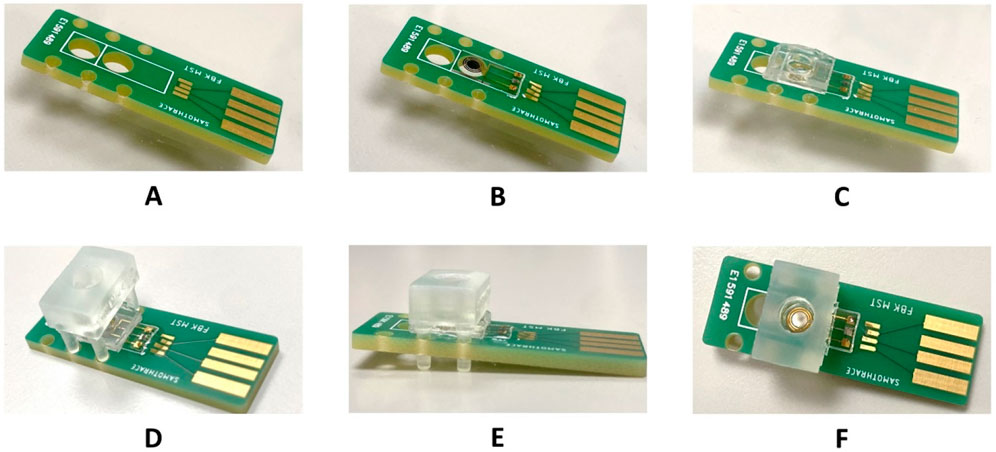
Figure 2. Electrochemical sensor assembly process. (A) A 12 mm × 35 mm customized PCB to host the electrode chip, (B) Electrode chip mounted on the PCB. (C) PDMS stamp mounted on the electrode chip. (D) Polycarbonate chamber aligned and placed on the assembly. (E) Side-view and (F) the top-view of the complete assembly.
2.3 Chip electrochemical characterization
The EC chip was electrochemically characterised by CV and EIS analysis. Measurements were performed by using the portable potentiostat PalmSens4 (PalmSens Instrument) assisted by PSTrace software and a USB connector properly fabricated. CV and EIS measurements were performed in drop casting mode using the [Fe(CN)6]4−/3− as redox probe. Actually, CV of 3 mm × 4 mm and 3 mm × 3 mm chip layouts were performed with concentrations of 0.05 mM and 1 mM redox probe dissolved in 0.2 M phosphate buffer (PB) at pH 6.8, at scan rates of 0.05, 0.1, 0.2 and 0.3 Vs−1 (covering a range widely used in sensing applications) and before and after a cleaning step with H2SO4 (described in the “Working electrode surface functionalization” section). EIS measurements were performed in drop casting mode using a 5 mM solution of [Fe(CN)6]4−/3− in 0.2 M of PB at pH 6.8. In the case of EIS measurements, a frequency range between 0.1 Hz and 100 kHz, 10 frequencies per decade, at an open circuit potential, with a voltage amplitude of 0.01 V, were used and the electron transfer process, [Fe(CN)6]3− + 1e− ⇄ [Fe(CN)6]4−, has been studied using EIS (Nicholson and Shain, 1964; Randviir, 2018). The experimental data obtained with the two systems described above were fitted using the PSTrace 5.10 software to a common Randles circuit, schemed in Figure 3. This equivalent circuit, which is one of the simplest possible models describing processes at the electrochemical interface, involves an active electrolyte resistance RS in series with the parallel combination of the double-layer capacitance constant phase element (CPE). To the above-mentioned components, the charge transfer resistance (Rct) and the Warburg impedance (W) were added. The latter is related to the electron transfer process and the diffusivity of the redox probe between the solution and the electrode surface, respectively.
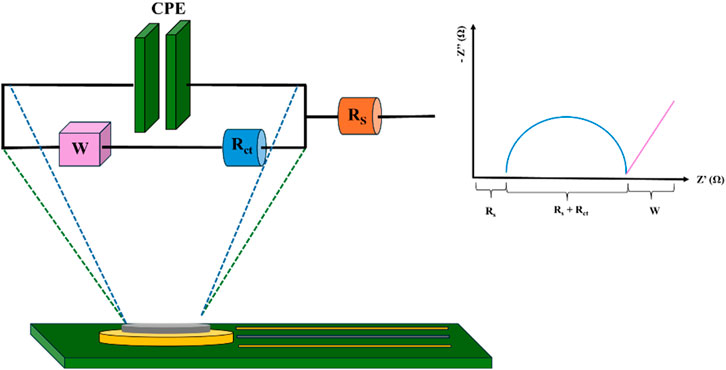
Figure 3. Schematic representation of the equivalent Randles circuit. Rs: Ohmic resistance; Rct: charge transfer resistance; W: Warburg impedance; CPE: constant phase element. Figure freely inspired by (Cancelliere et al., 2021).
CV measurements were performed in the range −0.35 to +0.6 V vs. reference electrode with different scan rates (from 0.05 V/s to 0.3 V/s). Furthermore, the Randles-Ševčík equation (Equation 1) was used to determine the electrochemically effective surface area (A) and the diffusion coefficient (D0) of 3 × 3 and 3 × 4 lab-on-chip sensors, as previously reported (Nicholson and Shain, 1964; Malvano et al., 2016):
where F is the constant of Faraday (mol−1), R the universal constant of gas (J/Kmol), n the number of exchanged electrons, A the electrode surface (cm2), C the analyte concentration (mol/cm3), D0 the diffusion coefficient (cm2/s), and ν the scan rate (0.1 V/s).
2.4 Oligonucleotide probes
For the functionalization test, oligonucleotide sequences of about 20 bases were immobilized on top of the chip platinum working electrode and used as probes in a final sensing array. At the 5′ end of the probe, a hexyl pendant (C6) was added as spacer for the right orientation once anchored to the electrode surface, while the thiol group (HS-) was used to functionalize the electrode surface, by inducing the thiol-Pt complex and the self-assembled monolayer (SAM) formation. The probes were used at a concentration of 1 µM.
2.5 Working electrode surface functionalization
The chip WE surface was modified by anchoring oligonucleotide probes as follows. The surface was cleaned by treating with 0.05 M H2SO4 and performing 10 cycles of cyclic voltammetry in the range of −0.6 V to +0.6 V, then dried with Ar gas. Hence, the devices were incubated with a mix solution (1:10 ratio) of thiol-modified probe 1 μM, suspended in PBS 10 mM at pH = 6.0, and 10 μΜ of 6-mercapto-1-hexanol (C6H14OS), dissolved in 10 mM PBS at pH = 6.0, at 25°C, 90% RH for 4 h with 60 rpm of stirring. Once functionalized with probe and thiol, the electrode surface was washed with PBS at pH 6.0.
2.6 Contact angle analysis
The wettability of the chip’s Pt surface was evaluated using a contact angle OCA25 system from DataPhysics. The CA, as a function of the surface wettability after each modification step, was assayed in drop casting mode using 1 µL of ultrapure water and analysing the drop age at 4 time points (0, 68, 134, and 203 s).
3 Results and discussion
The miniaturized electrode chips with two different configurations were successfully fabricated, each consisting of three electrodes arranged in a concentric circle layout, having the platinum working electrode in the centre. The reference and counter electrodes are patterned in gold. The key differentiator between the 3 × 3 and 3 × 4 chips is the surface area of the working electrode, that is 1.54 mm2 and 3.14 mm2, respectively. The electrode chips were mounted on PCBs and assembled for chip characterization and functionalization, as shown in Figure 4.
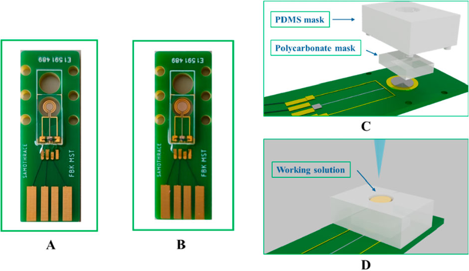
Figure 4. (A) 3 × 3 miniaturized EC chip; (B) 3 × 4 miniaturized EC chip (C) chip assembly with PDMS and polycarbonate masks; (D) working electrode reaction chamber for characterizations and functionalization.
Once assembled, two configurations of EC chips, 3 × 3 and 3 × 4, were fully characterized to evaluate their robustness, reproducibility and sensitivity. These two types of chips were first characterized by CV using both 0.05 and 1 mM solutions of [Fe(CN)6]3−/4− in 0.1 M KCl and 0.2M Pb and applying a scan rate of 0.1 V s−1. The obtained results were compared (solid and dashed lines of Figures 5A, 6A). In the presence of the electrolyte, there were well-defined [Fe(CN)6]3−/4− redox peaks in the CV responses for both EC chip configurations. However, the anodic and cathodic peak currents produced in 3 × 4 (Figure 5A) were higher due to a larger electrode surface area (Kang et al., 2010) that increased the background current.
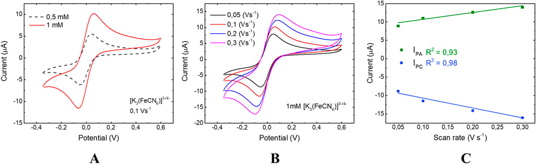
Figure 5. CV of 3 × 4 chip: (A) analysis at 0.5 mM and 1 mM concentrations of [Fe(CN)6]4−/3−; (B) response at scan rates of 0.3 (purple line), 0.2 (blue line), 0.1 (red line) and 0.05 (black line) Vs−1; (C) study of linear dependence between Ipa and Ipc. The error bars in the panel are the standard deviations calculated across three independent electrodes for each tested condition.
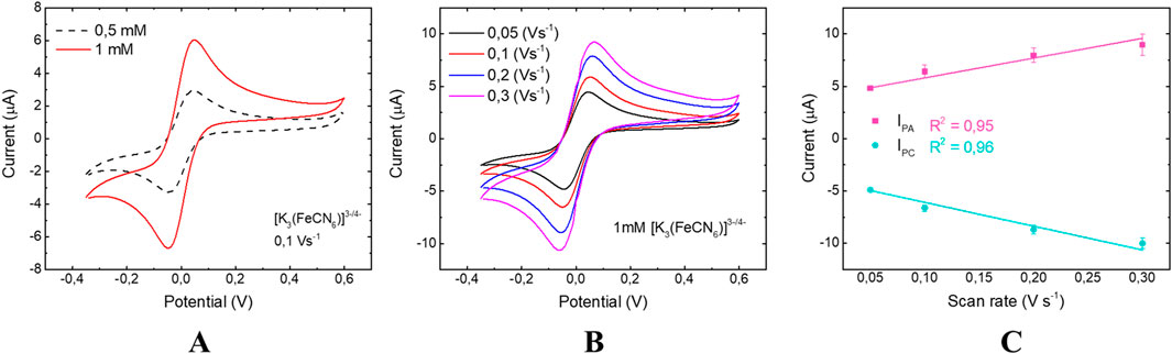
Figure 6. CV of 3 × 3 chip: (A) analysis at 0.5 mM and 1 mM concentrations of [Fe(CN)6]4−/3−; (B) response at various scan rates of 0.3 (purple line), 0.2 (blue line), 0.1 (red line) and 0.05 (black line) Vs−1; (C) study of linear dependence between Ipa and Ipc. The error bars in the panel are the standard deviations calculated across three independent electrodes for each tested condition.
These first results allowed us to study the nature of the electrochemical process occurring on the surface of the platinum WE, so the effect of the scan rate on the redox peak currents was investigated.
As shown in Figures 5B, 6B, the higher the scan rates, the smaller the diffusion layer size, and consequently the higher the current values. Since [Fe(CN)6]4−/3− is a reversible and freely diffusing redox species, the Randles-Ševčík equation (Equation 1) describes how the anodic and cathodic peak currents (Ipa, Ipc) increase with the scan rate. Plotting Ipa and Ipc as a function of the scan rate (Figures 5C, 6C), a linear dependence is observed for both EC chip configurations. This behavior indicates that the oxidation/reduction reactions of [Fe(CN)6]4−/3− are mainly diffusion-controlled in agreement with planar diffusion-controlled processes (Zoski, 2006).
By further manipulating Equation 1, the diffusion coefficient (D0), was calculated and reported in Table 1. In particular, the anodic (DA) and cathodic (DC) diffusion coefficients (D0) of [Fe(CN)6]4−/3− were calculated using 0.1 V/s as scan rate for the two configurations. The results were compared with the Konopka (DA = 7.26 ⋅ 10−6 cm2/s) and McDuffie (DC = 6.67⋅10−6 cm2/s) coefficients (Konopka and McDuffie, 1970).

Table 1. Diffusion coefficient (D0) estimated for 3 × 3 mm and 3 × 4 mm sensor using CV. Average values of at least 3 sensors are presented.
The data reported in Table 1 highlight that both the EC chips exhibit diffusive characteristics very similar to those of Konopka and McDuffie, but with a small difference in the 3 × 4 mm configuration, due to the larger active surface area. These CV analyses proved the effect of the redox analyte surface diffusion on the EC chip functioning.
Lastly, the behaviour of both EC chip configurations after sulfuric acid treatment was evaluated, and the results are reported in Figure 7. Also, for this characterization, CV and EIS were used as complementary tools to deeply characterize the electrochemical behavior of the electrode/electrolyte interface before and after the activation of the thiol groups with sulfuric acid.
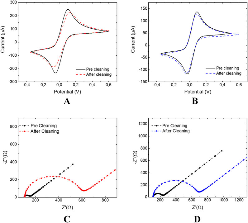
Figure 7. Characterization of EC 3 × 4 and 3 × 3 chip: CV pre and after cleaning with H2SO4 performed on 3 × 4 (A) and 3 × 3 (B) chips; EIS pre and after cleaning with H2SO4 performed on 3 × 4 (C) and 3 × 3 (D) chips.
The potential difference between the anodic and cathodic peak currents ΔΕ, Figures 7A,B, and the charge transfer resistance Rct, Figures 7C,D, calculated using CV and EIS, showed an increase of ΔΕ and Rct values compared to the bare platforms, Table 2. This trend indicates the formation of a platinum oxide layer (Díaz et al., 2009) that slows down the electron transfer. Furthermore, treatment with sulfuric acid allowed activation of the thiol groups on the surface and consequently modification of the electrical properties of the sensors. These outcomes are also confirmed by the calculated electrode active surface area (A in Table 2), which was reduced, after treatment with 0.05 M H2SO4, from 0.125 (bare) to 0.120 cm2 for the 3 × 3 mm configuration and from 0.241 (bare) to 0.220 cm2 for the 3 × 4 mm configuration, Table 2.
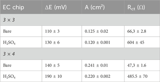
Table 2. Peak-to-peak separation ΔE, active surface area (A) and Charge transfer resistance (Rct), estimated for 3 × 3 and 3 × 4 EC chips.
Once fully characterized, the chip was tested to validate the functionalization of a probe sensing array on top of the platinum WE surface, as a first trial of chip suitability for NA sensing applications in a LoC format. Figure 8 of CA data reports that the contact angle of the bare surface was approximately 73.76° ± 7.0°, due to the rough surface of the platinum electrode, in agreement with literature (Yang et al., 2023). Then, the H2SO4 treatment of WE surface caused an improvement of the hydrophilicity of 3 × 4 mm sensors (58.97° ± 5.8°), suggesting the presence of platinum oxide (Zhang et al., 2015).
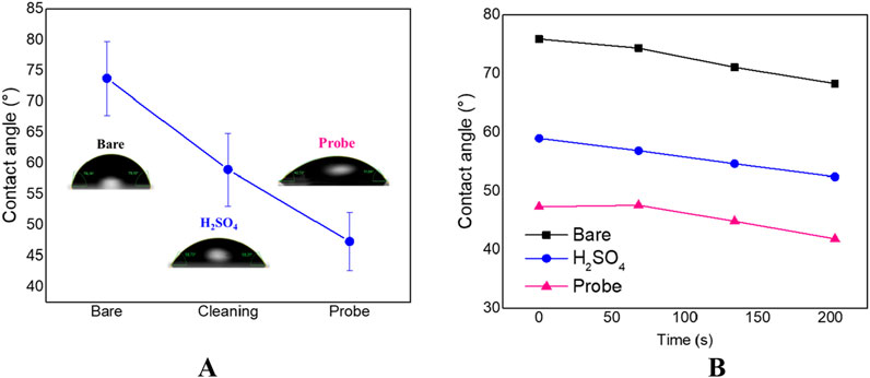
Figure 8. Wettability trend (A) and time-dependent CA modification (B) on oligo-functionalized chip.
After the anchoring of probe-thiol mix (ratio 1:10), the chip surface wettability increased (47.30° ± 4.7°), due to the abundance of polar groups (the main of which are OH and PO43− groups) coming from the immobilized probes (Bergese et al., 2009) and the thiol molecule (Calorenni et al., 2023).
4 Conclusion
A miniaturized EC chip for LoC application of NA sensing was presented. The electrode chips were fabricated using standard micromachining tools and technologies in a cleanroom environment, resulting in an overall production yield of 95%.
A deep characterization of chip layouts allowed identification of the best electrode configuration that responded properly to an electrochemical stimulus. More precisely, the analysis performed at different electro-active analyte concentrations reported the expected trend with an increase in anodic current, proving the responsivity of the chip surface. The CV performed at different scan rates confirmed the optimal electrochemical performances due to the absence of electrical noise at higher scan rates.
Lastly, the CV and EIS analysis before and after the electrodes cleaning reported a stable current peak, without any voltage shift or change of curve shape, and a good response to the surface electric modification, as reported by the EIS resistance marked increase measured after cleaning, proving the robustness of the WE surface towards the acidic treatment. Additionally, the trend of resistance values recorded at different [Fe(CN)6]4−/3− concentrations corroborated the chip’s responsivity to the redox probes.
In parallel, the CA analysis of the functionalized chip revealed a good enhancement of the WE surface wettability, as expected by the induced polarity by anchored oligonucleotide probes, proving the effectiveness of functionalization and the chip’s suitability for the NA sensing array preparation on a miniaturized device towards LoC molecular diagnostics applications.
Data availability statement
The raw data supporting the conclusions of this article will be made available by the authors, without undue reservation.
Author contributions
GB: Data curation, Writing – original draft. PC: Data curation, Writing – original draft. NY: Investigation, Writing – original draft. ES: Investigation, Writing – original draft. AM: Methodology, Writing – review and editing. KB: Writing – review and editing, Methodology. LL: Writing – review and editing, Supervision. SC: Conceptualization, Writing – review and editing.
Funding
The author(s) declare that financial support was received for the research and/or publication of this article. This work has been funded by the European Union (Next-Generation EU) through the MUR-PNRR project SAMOTHRACE (ECS00000022).
Conflict of interest
Author AM was employed by STMicroelectronics.
The remaining authors declare that the research was conducted in the absence of any commercial or financial relationships that could be construed as a potential conflict of interest.
Generative AI statement
The author(s) declare that no Generative AI was used in the creation of this manuscript.
Publisher’s note
All claims expressed in this article are solely those of the authors and do not necessarily represent those of their affiliated organizations, or those of the publisher, the editors and the reviewers. Any product that may be evaluated in this article, or claim that may be made by its manufacturer, is not guaranteed or endorsed by the publisher.
References
Bergese, P., Oliviero, G., Colombo, I., and Depero, L. E. (2009). Molecular recognition by contact angle: proof of concept with DNA hybridization. Langmuir 25, 4271–4273. doi:10.1021/la900428u
Borriello, M., Tarabella, G., D’Angelo, P., Liboà, A., Barra, M., Vurro, D., et al. (2023). Lab on a chip device for diagnostic evaluation and management in chronic renal disease: a change promoting approach in the patients’ follow up. Biosensors 13, 373. doi:10.3390/bios13030373
BPtrends.com (2025). Is platinum more expensive than gold in 2025? BP Trends. Available online at: https://www.bptrends.com/is-platinum-more-expensive-than-gold/(Accessed May 15, 2025).
Calorenni, P., Bella, G., Nicolò, M. S., Sciuto, E. L., Balli, M. V., Valenti, G., et al. (2023). Advanced DNA–gold biointerface for PCR-free molecular detection of leishmania infantum. Adv. Mater. Interfaces, 2400642. doi:10.1002/admi.202400642
Cancelliere, R., Albano, D., Brugnoli, B., Buonasera, K., Leo, G., Margonelli, A., et al. (2021). Electrochemical and morphological layer-by-layer characterization of electrode interfaces during a label-free impedimetric immunosensor build-up: the case of ochratoxin A. Appl. Surf. Sci. 567, 150791. doi:10.1016/j.apsusc.2021.150791
Chen, C., Tan, R., Wong, L., Fekete, R., and Halsey, J. (2011). in Quantitation of MicroRNAs by real-time RT-qPCR. Editors P. C. R. Protocols, and D. J. Park (Totowa, NJ: Humana Press), 113–134.
Díaz, V., Real, S., Téliz, E., Zinola, C. F., and Martins, M. E. (2009). New experimental evidence on the formation of platinum superactive sites in an electrochemical environment. Int. J. Hydrogen Energy 34, 3519–3530. doi:10.1016/j.ijhydene.2009.02.008
Gao, B., He, Z., He, B., and Gu, Z. (2019). Wearable eye health monitoring sensors based on peacock tail-inspired inverse opal carbon. Sensors Actuators B Chem. 288, 734–741. doi:10.1016/j.snb.2019.03.029
Golosov, D. A., Okojie, J. E., Zavadski, S. М., Rudenkov, А. S., Melnikov, S. N., and Kolos, V. V. (2018). Stability of the platinum electrode during high temperature annealing. Thin Solid Films 661, 53–59. doi:10.1016/j.tsf.2018.06.049
Hu, Y., Lan, W., and Miller, D. (2017). “Next-generation sequencing for MicroRNA expression profile,” in Bioinformatics in MicroRNA researchJ. Huang, G. M. Borchert, D. Dou, J. (Luke) Huan, W. Lan, and M. Tan, (New York, NY: Springer), 169–177.
Kang, X., Wang, J., Wu, H., Liu, J., Aksay, I. A., and Lin, Y. (2010). A graphene-based electrochemical sensor for sensitive detection of paracetamol. Talanta 81, 754–759. doi:10.1016/j.talanta.2010.01.009
Konopka, S. J., and McDuffie, B. (1970). Diffusion coefficients of ferri- and ferrocyanide ions in aqueous media, using twin-electrode thin-layer electrochemistry. Anal. Chem. 42, 1741–1746. doi:10.1021/ac50160a042
Lim, L. P., Lau, N. C., Garrett-Engele, P., Grimson, A., Schelter, J. M., Castle, J., et al. (2005). Microarray analysis shows that some microRNAs downregulate large numbers of target mRNAs. Nature 433, 769–773. doi:10.1038/nature03315
Malvano, F., Albanese, D., Pilloton, R., and Di Matteo, M. (2016). A highly sensitive impedimetric label free immunosensor for Ochratoxin measurement in cocoa beans. Food Chem. 212, 688–694. doi:10.1016/j.foodchem.2016.06.034
Najjar, D., Rainbow, J., Sharma Timilsina, S., Jolly, P., de Puig, H., Yafia, M., et al. (2022). A lab-on-a-chip for the concurrent electrochemical detection of SARS-CoV-2 RNA and anti-SARS-CoV-2 antibodies in saliva and plasma. Nat. Biomed. Eng. 6, 968–978. doi:10.1038/s41551-022-00919-w
Nelson, P. T., Baldwin, D. A., Scearce, L. M., Oberholtzer, J. C., Tobias, J. W., and Mourelatos, Z. (2004). Microarray-based, high-throughput gene expression profiling of microRNAs. Nat. Methods 1, 155–161. doi:10.1038/nmeth717
Nicholson, R. S., and Shain, I. (1964). Theory of stationary electrode polarography. Single scan and cyclic methods applied to reversible, irreversible, and kinetic systems. Anal. Chem. 36, 706–723. doi:10.1021/ac60210a007
Omar, C., Freisa, M., Man, H. M., Kechkeche, D., Dinh, T. H. N., Haghiri-Gosnet, A.-M., et al. (2024). Optimizing tris(2-carboxyethyl)phosphine and mercaptohexanol concentrations for thiolated oligonucleotide immobilization on platinum electrodes in microfluidic platforms. Langmuir 40, 26616–26625. doi:10.1021/acs.langmuir.4c03566
Pandey, I., Tiwari, J. D., Furukawa, H., Khosla, A., and Sekhar, P. K. (2022). Flexible Prussian blue/Carbon dots nanocomposite modified exfoliated graphite paper based sensor for simultaneous monitoring of hypertension and Parkinson disease. Microsyst. Technol. 28, 109–119. doi:10.1007/s00542-019-04468-2
Park, J., Lee, W., Lee, G., Choi, H., Kim, M., Kim, W., et al. (2019). Electrochemical amyloid-based biosensor for the determination of metal ions. J. Electrochem. Soc. 166, B1497–B1505. doi:10.1149/2.0451915jes
Pereira, R. L., Oliveira, D., Pêgo, A. P., Santos, S. D., and Moreira, F. T. C. (2023). Electrochemical miRNA-34a-based biosensor for the diagnosis of Alzheimer’s disease. Bioelectrochemistry 154, 108553. doi:10.1016/j.bioelechem.2023.108553
Petralia, S., and Conoci, S. (2017). PCR technologies for point of care testing: progress and perspectives. ACS Sens. 2, 876–891. doi:10.1021/acssensors.7b00299
Randviir, E. P. (2018). A cross examination of electron transfer rate constants for carbon screen-printed electrodes using Electrochemical Impedance Spectroscopy and cyclic voltammetry. Electrochimica Acta 286, 179–186. doi:10.1016/j.electacta.2018.08.021
Schmittgen, T. D., Lee, E. J., Jiang, J., Sarkar, A., Yang, L., Elton, T. S., et al. (2008). Real-time PCR quantification of precursor and mature microRNA. Methods 44, 31–38. doi:10.1016/j.ymeth.2007.09.006
Sciuto, E. L., Leonardi, A. A., Calabrese, G., Luca, G. D., Coniglio, M. A., Irrera, A., et al. (2021). Nucleic acids analytical methods for viral infection diagnosis: state-of-the-art and future perspectives. Biomolecules 11, 1585. doi:10.3390/biom11111585
Sierra, J., Marrugo-Ramírez, J., Rodriguez-Trujillo, R., Mir, M., and Samitier, J. (2020). Sensor-integrated microfluidic approaches for liquid biopsies applications in early detection of cancer. Sensors 20, 1317. doi:10.3390/s20051317
Srikanth, S., Jayapiriya, U. S., Dubey, S. K., Javed, A., and Goel, S. (2022). A lab-on-chip platform for simultaneous culture and electrochemical detection of bacteria. iScience 25, 105388. doi:10.1016/j.isci.2022.105388
Yang, B., and Agrios, A. G. (2018). Attachment of Pt nanoparticles to a metal oxide surface using a thiol–carboxyl bifunctional molecule. J. Colloid Interface Sci. 513, 464–469. doi:10.1016/j.jcis.2017.11.058
Yang, L., Lopes, I. C., and Vadgama, P. (2023). Self-cleaning sensors based on thermoresponsive polymeric film modified screen-printed platinum electrodes. Chem. Eng. J. 474, 145932. doi:10.1016/j.cej.2023.145932
Zhang, W., Bas, A. D., Ghali, E., and Choi, Y. (2015). Passive behavior of gold in sulfuric acid medium. Trans. Nonferrous Metals Soc. China 25, 2037–2046. doi:10.1016/S1003-6326(15)63813-4
Zhu, C., Hu, A., Cui, J., Yang, K., Zhu, X., Liu, Y., et al. (2019). A lab-on-a-chip device integrated DNA extraction and solid phase PCR array for the genotyping of high-risk HPV in clinical samples. Micromachines (Basel) 10, 537. doi:10.3390/mi10080537
Keywords: lab-on-a-chip, genetic analysis, electrochemical impedance spectroscopy, cyclic voltammetry, PCR-free analysis
Citation: Bella G, Calorenni P, Yadav N, Sciuto EL, Messina AA, Buonasera K, Lorenzelli L and Conoci S (2025) Development of a miniaturized electrochemical biochip. Front. Lab Chip Technol. 4:1611743. doi: 10.3389/frlct.2025.1611743
Received: 14 April 2025; Accepted: 26 May 2025;
Published: 04 June 2025.
Edited by:
Valentina Preziosi, University of Naples Federico II, ItalyReviewed by:
Hui Li, Southern Illinois University Carbondale, United StatesMario Barra, National Research Council (CNR), Italy
Copyright © 2025 Bella, Calorenni, Yadav, Sciuto, Messina, Buonasera, Lorenzelli and Conoci. This is an open-access article distributed under the terms of the Creative Commons Attribution License (CC BY). The use, distribution or reproduction in other forums is permitted, provided the original author(s) and the copyright owner(s) are credited and that the original publication in this journal is cited, in accordance with accepted academic practice. No use, distribution or reproduction is permitted which does not comply with these terms.
*Correspondence: Neeraj Yadav, bnlhZGF2QGZiay5ldQ==; Emanuele Luigi Sciuto, ZW1hbnVlbGVsdWlnaS5zY2l1dG9AdW5pbWUuaXQ=
†ORCID: Giovanni Bella, orcid.org/0000-0001-6646-3495; Katia Buonasera, orcid.org/0000-0001-5695-7061