 Zixian Wang
 Lin Sun1,2,3
 Wentao Xu
- 1Institute of Photoelectronic Thin Film Devices and Technology, Nankai University, Tianjin, China
- 2Key Laboratory of Optoelectronic Thin Film Devices and Technology of Tianjin, Nankai University, Tianjin, China
- 3Engineering Research Center of thin film optoelectronics technology, Ministry of Education, Nankai University, Tianjin, China
Flexible electronics has attracted tremendous attention in recent years. The essential requirements for flexible electronics include excellent electrical properties, flexibility and stretchability. By introducing special structures or using flexible materials, electronic devices can be given excellent flexibility and stretchability. In this paper we review the realization of flexible electronics from the perspective of structural design strategies and materials; then, healthcare application of flexible electronic systems was introduced. Finally, a brief summary and outlook are presented.
Introduction
Flexible electronics has attracted tremendous attention in recent years. Development of flexible and stretchable devices, which are the basis of flexible electronics, has recently become one of the research focuses (Wong et al., 2009; Yao et al., 2016; Trung and Lee, 2017; Long et al., 2012; Liu et al., 2017; Li et al., 2016; Boutry et al., 2015). Flexible electronic devices use organic or inorganic electronic materials on flexible substrates (Gates, 2009). Flexible electronic devices have been developed since the early 20th century. The first flexible electronic device was a radio tuner composed of graphite paste (Seymour, 1927). The discovery of conductive polymers (Shirakawa et al., 2003) increased the attention paid to development of flexible electronics. Recent use of materials including graphene and carbon nanotubes in flexible sensing and optoelectronic devices has greatly promoted the development of flexible electronics (Shen and Fan, 2016). Flexible electronics has received widespread attention because of its excellent stretchability while maintaining electrical properties and have application prospects in various fields such as flexible transistors (Sirringhaus et al., 2000; Forrest, 2004; Sandström et al., 2012) pressure sensors (Chang et al., 2009), light-emitting diodes, and so on.
Much current research on flexible electronics focuses on integrating flexible electronic devices, and on developing flexible semiconductor materials that have high chemical stability, high electrical conductivity and low price. Organic semiconductors such as pentacene are the first to be considered due to their good compatibility with flexible substrates. However, the chemical and electrical properties of organic semiconductors need to be further improved. Compared with organic flexible electronics, inorganic rigid electronics with special structure have good electrical properties. Here, we review development of materials and processes to realize flexible electronic devices; then we survey healthcare applications of typical flexible electronic devices.
Basic Structure of Flexible Electronic Devices
Generally, flexible electronic devices include at least four parts: electronic components, flexible substrates, cross-linked conductors, and sealing layers (Wong et al., 2009). The parts are combined using an adhesive layer, so the adhesive must be sufficiently strong, flexible, and chemically stable. However, choice of adhesive must consider the manufacturing process. For example, transfer printing is required in the production process of inorganic flexible electronics (detailed introduction in From the Perspective of Structural Design). The transfer process exploits the difference in adhesion between the device, the stamp and the substrate, and this usage imposes requirements on the characteristics of the adhesive layer. Also, some electronic components are sensitive to water and oxygen, so they must be protected using a special sealing layer.
Electronic Components
Electronic components can realize functions such as information storage and calculation. Unlike traditional electronic components, flexible electronic components can be composed of organic materials. Unlike traditional electronic components, flexible electronic components can be composed of organic materials and can be directly distributed on a flexible substrate. For example, thin film transistors have excellent flexibility, so they can maintain their electrical characteristics under certain external forces. However, the stability and electrical characteristics of organic material transistors are inferior to those of silicon transistors. Electronic components made of inorganic semiconductor materials such as silicon are brittle, so they will break when flexed. Special structures to achieve flexibility have been fabricated, such as island-interconnect design (Kim et al., 2012). We will introduce them in detail in the following sections.
Flexible Substrate
Flexible substrates are the biggest difference between flexible electronics and rigid electronics. Flexible substrates must also be insulative and inexpensive. Therefore, development of flexible electronics imposes strong constraints on material selection and on the process of manufacturing the substrate. At present, flexible substrates are mainly divided into two categories: polymer substrates and stainless-steel foil substrates (detailed introduction in Flexible Substrate).
Flexible substrates have advantages. They are not structurally damaged or broken by application of external forces. Different flexible substrates can be chosen according to the usages of the device. For example, PDMS is used as the substrate for electronic skin, whereas PET is used as a flexible substrate in flexible electronic displays. Flexible substrates are also thin and light: to achieve the required flexibility, they have been made as thin as possible. This trait reduces the weight of the device and the cost of materials. Flexible substrates are also compatible with roll-to-roll production, and therefore have potential for industrial mass-production.
Flexible substrates also have shortcomings. Their surfaces are relatively rough. Also most polymer substrates decompose when exposed to air or certain chemical agents. Both of these traits degrade the electrical characteristics of devices that use the flexible substrates.
Cross-Linked Conductor
In the island-interconnect structure (detailed introduction in Island-Interconnect Design), each electronic component exists as in an isolated device island, and cross-linked conductors connect the electronic components to form a complete flexible circuit. At present, metal conductors are the most common conductors; among them, copper foil is most widely used due to its low price, good conductivity and good ductility. Rolled copper foil and electrolytic copper foil are the two most common types of copper foil; of the two types, rolled copper foil has better conductivity and ductility (Table 1).
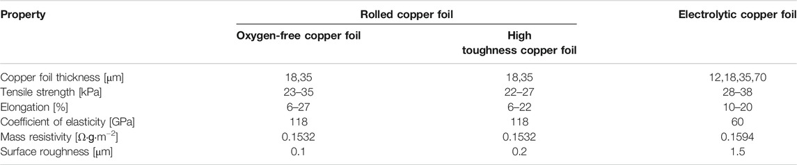
TABLE 1. Main properties of copper foil.
Sealing Layer
The sealing layer is used to protect flexible electronic devices from damage by dust, water, gases, and mechanical forces. The sealing layer must maintain good electrical stability when subjected to large bending deformations, and this requirement constrains the choice of materials used. Acrylic resin, epoxy resin, and polyimide are commonly used, but their chemical stability is insufficient to ensure adequate service life of flexible devices.
The sealing layer also affects the stretchability and flexibility of flexible electronic devices. Therefore, the structural design of the sealing layer must be optimized so that the electronic components can be located on the mechanically-neutral surface of the sealing layer. For example, in the island-interconnect structure, appropriate design of the structure of the sealing layer (Yoon et al., 2007): can reduce the stress on the edge of the cell island to increase the mechanical toughness of the flexible device, and prevent separation of electronic components and flexible substrates to extend the service life of flexible devices.
Flexible electronic devices in different applications have different requirements for the sealing layer. For example, organic light-emitting diodes (OLEDs) have high requirements for sealing, but thin film transistor (TFT) devices and liquid crystal displays (LCDs) devices have low requirements for sealing. Different flexible electronic devices have different requirements for air and water permeability of the encapsulation layer. Water and oxygen can ruin the performance of OLEDs, LEDs and solar cells, so the water and oxygen permeability of the encapsulation materials in these devices should be very low. For instance, the water vapor transmission rates (WVTR) should be less than 10−6 g/m2/day and the oxygen transmission rates (OTR) should be less than 10−5 ml/m2/day for OLEDS with a service life greater than 10,000 h. However, in order to relief the discomfort caused by the accumulation of water vapor on the skin surface, encapsulation materials need possess high water and oxygen permeability for wearable flexible electronic devices. The common WVTR is around 100–1,000 g/m2/day, which meets the WVTR requirements of normal skin (240–1920 g/m2/day) (Li et al., 2020). The encapsulation of flexible electronics cannot use traditional methods and requires the use of thin-film encapsulation, which can meet the requirements of the device for flexibility. For equipment with high sealing requirements, the sealing can be improved by increasing the film density and adopting a multi-layer structure.
Flexible Realization
The discovery of conductive polymers is regarded as the beginning of organic electronics, and since that event, organic semiconductors have been intensively studied. Various organic small molecules and polymer semiconductors have been applied to thin film transistors (Dadvand et al., 2013; Li et al., 2017). So far, the mobilities of p-type and n-type polymer semiconductor films have exceeded 35 cm2/(V·s) and 5 cm2/(V·s), respectively. However, the carrier mobility, switching ratio and stability of organic semiconductors must be further improved, because flexible electronics based on inorganic materials have advantages in electrical properties. The concept of stretchable and flexible electronics (Khang et al., 2006) has stimulated research on flexible electronics. Next, we will introduce the realization of flexible electronics from two aspects: materials and process technology.
Flexible Material
To obtain flexibility and integrity of the entire device, conductor materials, semiconductor materials and dielectric layer materials must all be sufficiently flexible.
Flexible Substrate
The choice of substrate material is critical to the flexibility of the device. The most commonly-used flexible substrates are composed of polymers, such as polyethylene terephthalate (PET) (Phan et al., 2017), polyethylene-2, 6-naphthalate (PEN) (Fleischhaker et al., 2010; Kwon et al., 2014), polydimethyl siloxane (PDMS) (Bae et al., 2013; Amjadi et al., 2014; Pal et al., 2018), and polyimide (PI). The flexibility of the substrate or device can be evaluated by measuring its mechanical stability under upward or downward arch deformation (Jedaa and Halik, 2009). The flexibility of the substrate increases as its thickness decreases.
A flexible substrate should also tolerate reasonably high temperatures. For example, PI can withstand a temperature of 450°C. In some special applications, the substrate must have good biocompatibility.
Flexible Conductor
Flexible conductors include electrodes of flexible electronic devices, and wires that are used to connect devices. Common flexible conductor materials include silver nanowires (Lee P et al., 2012; Amjadi et al., 2014), carbon nanotubes (Lipomi et al., 2011), graphene (Chen et al., 2011; Feng et al., 2016), carbon grease (Pelrine et al., 2000), conductive polymer (Groenendaal et al., 2000), and liquid metal (Park et al., 2012). In theory, all of these materials can be used as electrodes for devices, but different conductors will produce different carrier injections; therefore, when selecting materials, a conductor material that matches the semiconductor should be preferred. Metal conductors are prone to break when they are deformed, but their flexibility can be improved by appropriate design, for example, a fractal structure (Rogers et al., 2010). Graphene is widely used as an electrode material in batteries and supercapacitors, because it has excellent electrical and optical properties. Redox graphene has been used to prepare flexible capacitors that retain excellent electrical properties even after a 180° bend (Jiang et al., 2019). Soft lithography has been used to fabricate capacitive pressure sensing skins with liquid alloys as electrodes (Wong et al., 2012).
Flexible Semiconductors
Flexible semiconductor materials can be divided into three categories: inorganic, organic, and metal oxide.
Inorganic semiconductor materials have excellent piezoelectric properties and are widely used in flexible sensors (Kim and Rogers, 2008). Indium zinc oxide (IZO) films have high carrier mobility and high light transmittance, so they are used in liquid crystal displays and solar cells. However, solutions of inorganic semiconductor materials are difficult to prepare, and the processing procedure is complicated.
Use of intrinsically flexible organic semiconductors is superior to use of inorganics. Flexible organic semiconductors are divided into two small-molecule type and high-polymer type. Triphenylamine and fullerene are typical small-molecule organic semiconductor materials. Copolymers are typical polymer semiconductor materials. The stability and electrical properties of organic semiconductors must be improved; the use of inorganic nanomaterials to modify organic semiconductors can significantly improve their electrical properties (Zheng et al., 2014).
Flexible Dielectric Layer
Dielectric materials are generally divided into inorganic materials and organic materials. Compared with inorganic materials, organic dielectric materials are easy to process and have excellent flexibility, showing great prospects in the field of flexible electronics. Styrene ethylene butylene styrene (SEBS) (Zhang et al., 2014b; Su et al., 2017), Poly (vinylidene fluoride-trifluoroethylene) (P(VDF-TrFE)) (Zhang et al., 2014a; Zheng et al., 2016), and Poly (methyl methacrylate) (PMMA) are common organic dielectric layer materials.
The structure and properties of the dielectric layer have a significant effect on the electrical properties. of the device. When the surface roughness of the dielectric increases, the p bonds on the surface of the dielectric layer overlap and thereby restrict the injection of carriers and reduce their mobility (Jung et al., 2008; Jung et al., 2010). Jung et al. spin-coated a layer of Poly (2, 5-bis (3-alkylthiophen-2-yl) thieno[3, 2-b]thiophene) (pBTTT) on the dielectric layer to reduce the roughness of the dielectric layer, which Improve the electrical properties of the device (Jung et al., 2008). The dielectric constant ε is also a very important indicator. Increased dielectric constant of a dielectric increases the charge that a given gate voltage can induce, so the electrical properties of the device is significantly improved. Although organic dielectrics have low operating voltages, they also have other drawbacks, such as unstable properties, high switching ratios, and low ion mobility. These problems can be lessened by amending the polymer with adjuvants such as x-PVP/OTS, Ta2O5/PMMA, and PDMS:BaTiO3.
Natural biological materials have good biological properties and degradability. In field effect transistors (FETs) that used pentacene and C60 and albumen as a dielectric layer, the capacitance of the albumen dielectric layer was 12.45∼13.25 nF/cm2, which is greater than that of PMMA (7.0∼7.9 nF/cm2) The FETs’ other electrical characteristics were also good (Figure 1). Use of critically dried flower petals as a medium layer material yielded high-performance piezoelectric electronic skin (Wan et al., 2018). The use of natural plant materials broadens the choice of flexible electronic materials; furthermore, plant materials have excellent biocompatibility, so they are applicable in implantable devices.
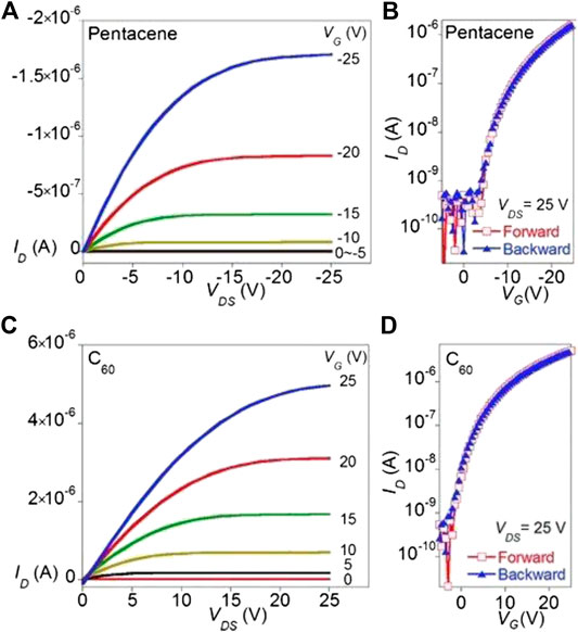
FIGURE 1. The electrical properties of FETs with albumen dielectrics (Chang et al., 2011). Reproduced with permission.
Flexible Electronics Processing Technology
At present, the processing methods of flexible electronics are mainly divided into two categories: making flexible materials into flexible electronic components; and preparing inorganic flexible electronics by structural design.
From the Perspective of Materials
Progress in materials science has yielded many intrinsically flexible materials that can be used in organic electronics (Nathan et al., 2012; Dodabalapur 2006). For example, use of pentacene as a semiconductor in a grid-like pressure sensor achieved drain current that maintained excellent stability when a 25% strain was applied to the device (Someya et al., 2005). Furthermore, the pressure and temperature sensors prepared by the same method were successfully integrated into the grid, and the whole system realized temperature and pressure sensing. Organic thin film transistors that had been fabricated in a double-layer structure using a laminating method (Figure 2) with polydimethylsiloxane as dielectric and polyisoindigodithiophene-siloxane as semiconductor (Schwartz et al., 2013) could work in a sub-threshold state, and had significantly improved sensitivity (8.4 kPa−1), response time (<10 mn) and working power (<1 mW). By adjusting the microstructured PDMS, the damage to the device by the external force can be significantly reduced, so after 15,000 pressure cycles, the electrical properties of the device was not significantly reduced.
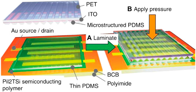
FIGURE 2. Schematic diagram of sensor structure. It is made by laminating two layers. The first contains the bottom source-drain electrodes and the semiconducting polymer, and the second contains the gate electrode and the microstructured dielectric. The thin PDMS layer on top of the semiconductor ensures a homogeneous dielectric interface and provides protection during the lamination step (Schwartz et al., 2013). Reproduced with permission.
The physical and chemical properties of materials are very different at the nanometer scale than at the bulk scale (Baca et al., 2008; Yang and Li, 2007). This principle has been exploited to realize a polymer semiconductor that exploits the nano-confinement effect (Xu et al., 2017).
A conjugated-polymer/elastomer process to induce elasticity by phase separation to prepare nano-constrained semiconductors can prevent cracks. DPPT - TT was used as a polymer semiconductor and SEBS was used as an elastomer; the diameter of the polymer fiber was <50 nm when the content of SEBS was 70%. When 100% stretching was applied, the electrical properties of the film were not significantly reduced, and remained three orders of magnitude larger than the film without SEBS; the film also did not show significant cracks after 100% stretching. Thin film transistors that had carbon nanotubes as electrodes and nano-constrained semiconductors retained good stability after 10,000 stretches to 25%, so they can withstand the usage scenarios of most wearable devices.
Inorganic materials can be used to demonstrate flexible electronics both directly and indirectly. The conductive inks can be printed on the flexible substrates directly to form the functional layers. Alternatively, the inorganic materials can be transferred onto the flexible substrates by transfer printing as well.
Inorganic conductive materials such as metal nanoparticles (Dearden et al., 2005; Shen et al., 2014; Öhlund et al., 2015; Woo et al., 2009; Kang et al., 2014), graphene, and carbon nanotubes (Kordás et al., 2006; Wei et al., 2007) have been made into conductive inks for printing flexible electronic devices. Printed electronics technology refers to fabrication of electronic devices by patterning with conductive ink. Printed electronics are mainly divided into two categories: contact printed and non-contact printed. Screen printing, compensation printing, and gravure printing are all contact printing, but their accuracy is difficult to control and the operation is complicated. Non-contact printing has incomparable advantages and has been widely used in the preparation of flexible electronics (Arias et al., 2008; Deganello et al., 2010; Nambiar and Yeow, 2011). For example, inkjet printing has been used to prepare thin film transistors on flexible (Lee S. K. et al., 2012). Non-contact printing technology is mainly divided into three categories: inkjet printing, electrohydrodynamic printing (EHD) and aerosol jet printing. Inkjet printing is to uses pressure to eject the ink to complete the printing process; common driving methods are the piezoelectric method and the thermal bubble method (Le, 1998). The accuracy of inkjet printing is easily affected by the surface tension and viscosity of the ink, so the parameters must be strictly controlled when printing. Electrohydrodynamic printing is a printing technology that has high precision (Park et al., 2007). It uses an electric field force: under the action of the electric field force, the ink droplet forms a Taylor cone at the nozzle; at the same time, due to the high electric potential at the nozzle, the ink droplet is subjected to electric shearing force, and when the electric field force exceeds the surface tension, the ink droplet exits the nozzle (Basaran, 2002). Aerosol jet printing is different from inkjet printing. The ink droplets are vaporized into small particles <5 μm, which are carried by high-speed airflow to the nozzle to complete the printing process. Aerosol printing has been widely adopted in the field of flexible electronics, such as for production of photovoltaic devices (King and Ramahi, 2009) and printing of optical waveguide devices (Reitberger et al., 2015).
Transfer printing is an emerging processing technology that is compatible with other micro-nano processing technologies and has been widely used in flexible electronics (Wang et al., 2017; Linghu et al., 2018; Huang et al., 2019). The typical transfer process includes four steps: 1) a special silicon wafer with a sacrificial layer need be prepared; 2) functional components are prepared on top by the traditional microelectronic processing technology; 3) the sacrificial layer is etched away; 4) the electronic components are finally peeled off from the rigid substate and transferred to the flexible substrate. The transfer processes involve multiple interfaces and thus are diverse, including speed separation, surface microstructure, tape transfer, and sacrificial layer.
From the Perspective of Structural Design
Flexibility of inorganic semiconductor devices can also be achieved by special structural design. The typical structure design is mainly divided into four categories: 1) Buckled Nanoribbons; 2) Island-Interconnect Design; 3) Serpentine-Interconnect Design; 4) Other Designs.
Buckled Nanoribbons
Inorganic materials have a certain degree of stretchability when they are thin enough, and their bending strength and bending strain increase as the film thickness decreases (Khang et al., 2009). A buckled nanoribbon structure was designed to exploit these characteristics; it uses sinusoidal nanoribbons that can be adapted to the strain applied to the plane by adjusting the wavelength and height of the convex portion. This buckling structure can be achieved by depositing a metal or silicon film on a prestrained PDMS elastic film; the specific contact between silicon nanoribbons and PDMS is achieved by -O-Si-O- bonds (Meitl et al., 2006; Sun et al., 2006; Sun and Rogers, 2007). For example, manufactured silicon nanobelts can be transferred from the silicon wafer surface to the PDMS by using a transfer-printing process (Khang et al., 2006) (Figure 3A); when this prestrain is released, the silicon nanobelt assumes a sinusoidal buckling structure (Figure 3B).
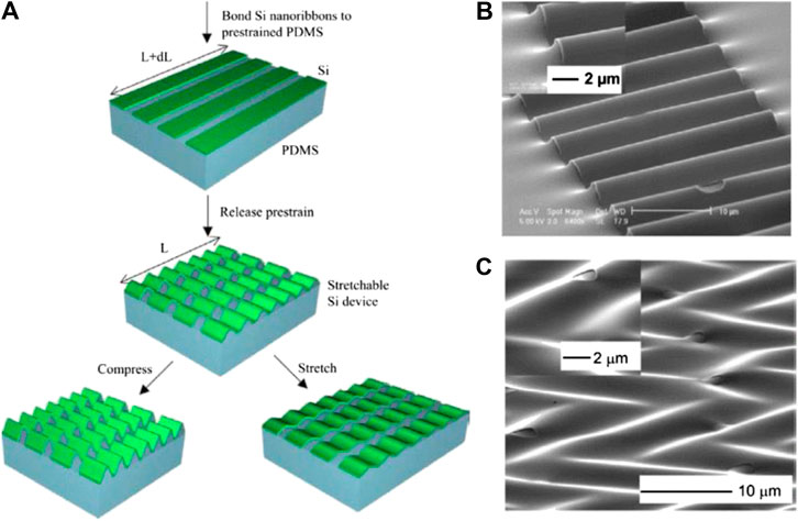
FIGURE 3. (A) Schematic illustration of the process for fabricating buckled wavy single-crystal silicon ribbons on a PDMS substrate. (B), (C) SEM images of stretchable nanoribbons and stretchable nanomembranes (Song et al., 2009). Reproduced with permission.
The same principle can be applied to a two-dimensional plane: when prestrains in the X-axis and Y-axis directions are simultaneously applied to the PDMS, a herringbone buckling structure can be produced (Figure 3C). Interestingly, compressibility and scalability show opposite trends with the magnitude of prestrain in this structure: as the prestrain increases, the compressibility decreases and the scalability increases; when the prestrain is 13.4%, the scalability and compressibility are equal.
To improve the stretchability of the device, the buckling structure of the nanoribbons has been optimized using pre-lithographic PDMS (Sun et al., 2006). The activated area (Figure 4A, purple area) can be tightly combined with the nanobelt, whereas in the unactivated area, the combination of the nanobelt and PDMS is easily broken (Figure 4A). When the prestrain is released, the PDMS at the activated part is tightly combined with the nanobelt and forms a buckled structure in the unactivated part (Figure 4C). The wavelength of the buckling nanobelt can be controlled by selective photolithography of PDMS. The contour lines of GaAs nanoribbons differ under different strains when the width of the activated area is 10 mm and the width of the inactive area is 190 mm (Figure 4E). The buckling structure greatly improves the stretchability of inorganic materials. For example, a sinusoidal silicon nanobelt can withstand a strain of ∼20% before breaking. Theoretical analysis and experiments show that for some specific materials, the buckling structure can increase its stretchability to 30%. The buckling process is compatible with traditional processes that use silicon wafers, so the buckling structure has been applied in flexible electronic devices (Kim et al., 2008a). However, although the buckled nanoribbons greatly improve the stretchability of rigid semiconductor materials, excessive prestrain affects the electrical properties of semiconductor materials.
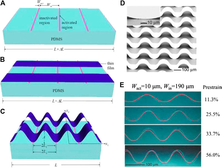
FIGURE 4. (A) Prestrained PDMS with periodic activated and inactivated patterns. (B) Thin film parallel to the pre-strain direction is attached to the prestrained and patterned PDMS substrates. (C) Relaxation of the pre-strain in the PDMS leads to buckles of the nanoribbons. (D) SEM image of buckled GaAs nanoribbons formed using (A)–(C). (E) Buckled GaAs thin films on patterned PDMS substrate for different prestrain levels. Red line: calculations; blue line: experimental data (Song et al., 2009). Reproduced with permission.
Island-Interconnect Design
The island-interconnect structure (Kim et al., 2012) solves the problem that excessive prestrain affects the electrical properties of semiconductor materials. The island-interconnect structure (Figure 5) is produced by transferring a pre-lithographic mesh structure to a biaxially-stretched PDMS, then the prestrain is released to bend the interconnecting conductors. Some parts develop weak bonds (Figure 5, green areas) and some develop strong bonds (Figure 5, cyan areas). The device adjusts the connecting conductor (Figure 5 green area) to adapt to the external force applied to the device and almost no deformation occurs on the islands (Figure 5 cyan areas). The stretchability of the structure depends on its degree of pre-strain, and the maximum stretch of the device is the degree before the strain is released (Figure 5, top frame). The compressibility and stretchability of electronic devices increase as the length of the interconnecting conductor increases; the flexibility of the structure can be controlled by adjusting the length of the conductor.
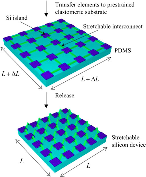
FIGURE 5. Schematic illustration of the process for fabricating electronics with the island–interconnect mesh designs on an elastomeric substrate (Song et al., 2009). Reproduced with permission.
Application of this structure has been extended to curved surfaces (Figure 6) (Ko et al., 2009). First, a PDMS film was cast on a curved surface, cured, and then removed. Second, radial stretching was applied to the PDMS film to convert the curved surface to a plane, then a pre-made circuit was transferred onto the strained PDMS. Third, the strain was released then the PDMS was fitted to a curved surface and the edges of the PDMS were removed. Due to the influence of the curved surface, the strain varies over the film. For example, the strain at the center position is 0 and the strain at a point on the outermost circumference is close to 60%. Therefore, after the strain is released, the shapes of the interconnection wires differ: one single arch structure is formed in the circumferential direction, a multi-arch structure is formed in the radial direction, and the interconnection wire at the center position is not deformed.
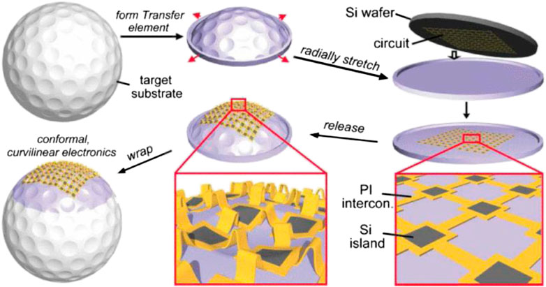
FIGURE 6. Schematic illustration of the steps for using silicon membrane circuits in mesh layouts (i.e., arrays of islands interconnected by narrow strips) and elastomeric transfer elements to wrap electronics onto substrates with complex curvilinear shapes, such as the dimpled surface of the golf ball shown here (Ko et al., 2009). Reproduced with permission.
The compressibility and stretchability of the island-interconnect structure increase with increase in the interconnection distance (Jiang et al., 2007). The requirement for a long interconnection limits the application of this structure in highly-arrayed devices. PDMS fabricated by soft lithography can be used as a substrate to fabricate a trench-type interconnection structure, with electronic components placed on raised islands (Figure 7) (Lee et al., 2011). This structure can autonomously control the location of islands and achieve a height array. After soft lithography, islands with a length of 800 μm and a width of 200 μm are separated by trenches that have a width of 156 μm (Figure 7A). In this structure, the island is less sensitive to the strain than the groove is: 20% strain applied to the PDMS is divided into 123% strain in the groove and 0.4% strain in the island (1/300 times the strain in the groove).
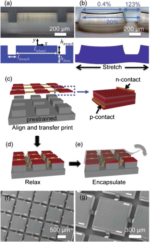
FIGURE 7. Optical microscopy images and FEA calculations of deformation of a slab of PDMS and schematic illustrations of the steps in the fabrication of stretchable GaAs photovoltaic modules with SEM images of a completed device. Cross-sectional optical microscopy images (top) and FEA (bottom) of a slab of PDMS in (A) relaxed and (B) stretched states, with a square array of raised islands separated by recessed trenches, designed as a platform for (C) stretchable inorganic photovoltaics with high areal coverages. (D) Releasing the prestrain and pressing on the entire array using a flat plate of glass deform the interconnects into arc shape, in a vertical downward orientation, into the trench regions of the PDMS substrate. (E) In a final step, a thin, uniform layer of PDMS is bonded on the top, as an encapsulant to protect the system from the environment. (F) and (G) SEM images of a completed module (Lee et al., 2011). Reproduced with permission.
Serpentine-Interconnect Design
The design of non-coplanar, serpentine metal interconnection can effectively solve the limitations of pre-stretching (Kim et al., 2008b). When the applied stretch reaches the prestrain, a serpentine metal can be further stretched by out-of-plane distortion. In a CMOS transistor that has a serpentine interconnect structure (Figure 8A), the serpentine structure is composed of a stack of polymer/metal/polymer materials. For a system with a prestrain of 35%, the serpentine structure can be stretched to 70%; at the same time, finite element analysis shows that the deformation peaks of the interconnecting metal and the metal in the island are 0.2% and 0.5%, respectively (Figures 8B,C). When the degree of prestrain is further increased, the stretchability of the structure can exceed 100%. This high degree of deformation is reversible; the electrical properties of the device do not change significantly after more than 10,000 stretches (Kim et al., 2008). Non-coplanarity is very important for serpentine interconnect structure; without prestrain, 60% stretching will cause 6.8% strain on coplanar structures (which will cause damage to the components on the island) and 0.18% strain on non-coplanar structures (Gray et al., 2004).
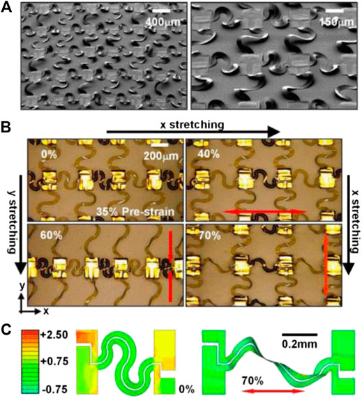
FIGURE 8. (A) SEM image of an array of stretchable CMOS inverters with noncoplanar bridges that have serpentine layouts (left) and magnified view (right). (B) Optical images of stretching tests in the x - and y -direction. (C) FEM simulation before (35% prestrain) and after (70% applied strain) stretching (Kim et al., 2008). Reproduced with permission.
Combining the advantages of the serpentine interconnects structure and the buckling structure can develop an ultrastretchable electronic system. Serpentine interconnect structure can be combined with to the prestrained PDMS (Figure 9A), and after the strain is released, the structure in the direction perpendicular to the tension (every corner of the serpentine structure) is compressed (Figure 9C). This structure can resist large strains by engaging in out-of-plane motion at the corners of the serpentine structure (Gray et al., 2004; Brosteaux et al., 2007; Gonzalez et al., 2008; Huyghe et al., 2008; Ershad et al., 2019). Without prestrain, the structure can withstand a maximum of 120% of stretching, whereas if a prestrain of 85% is applied, the serpentine interconnect structure can withstand a maximum of 280% of stretching. At the same time, the device has good reversibility, and the structure remained intact after 25,000 stretches of 185%.
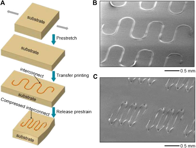
FIGURE 9. (A) Schematic illustration of the prestrain strategy for fabricating serpentine interconnects with enhanced levels of stretchability. (B) SEM image of the serpentine structures before releasing the prestrain of the substrate. (C) SEM image of the serpentine interconnect after releasing the prestrain of the substrate (Zhang et al., 2014). Reproduced with permission.
Other Designs
The fractal structure can increase the areal coverage of device by increasing the orders of fractal bridges (Song et al., 2016). The first-order fractal bridge has a serpentine structure and the higher-order fractal bridge has a similar structure to the previous one. Each fractal bridge is determined by six parameters: the width w and thickness t of the bridge, basic length l, fractal order n, the number of unit cells m, and the height/spacing ratio η. The width of the fractal bridge is an important parameter. For example, the scalability of the fractal bridge increases by nearly 8 times (from 2.3% to 17.6%) when w/l is reduced from 0.8 to 0.2. In addition, the fractal order n is the most important parameter. The elastic stretchability of the fourth order fractal bridge is 2,140%, which is nearly 20 times than that of the first order fractal bridge (10.7%). However, it is worth mentioning that the above-mentioned improvement in stretchability is for the fractal bridge, and this structure has limited improvement in the stretchability of the whole device. For example, when the fractal bridge with a stretchability of 1,000% covers 90% of active devices, the stretchability of the entire system is only 50%.
Direct patterning on the flexible substrate can omit the transfer printing process and thus simplify the production process (Cao et al., 2018). A special network polysulfide can be generated by tricyclic [5.2.1.02,6] dimethyl diacrylate and pentaerythritol tetrakis (3-mercaptopropionate) under the catalysis of triethylamine. Hydrogen peroxide can oxidize the sulfide and its glass transition temperature changed from 9°C to 63°C. Therefore, the oxidized substance is glassy and the non-oxidized substance is rubbery at room temperature. Based on this principle, the sulfide substrate is oxidized in a controlled manner and then the active device is fabricated at the oxidized position. As a result, the device prepared in this way can isolate the strain from the active region. When the flexible temperature sensor made in this way stretches to 40% of the entire device, the maximum strain of the protected area is only 0.15%. compared to the situation without protection, the strain at all positions is 5% when a 5% stretch is applied.
The strategy of using flexible materials to prepare flexible electronics is relatively simple, but the electrical properties and stability of the device needs to be further improved; although the production of flexible inorganic electronics is complicated, it maintains excellent electrical properties, and the stretchability of inorganic electronics has been increased to 300% in the past ten years (Wang S. et al., 2015). Flexible electronics is an interdisciplinary field including electronics, materials science, chemistry and mechanics. We believe that with the development of research in related fields, the electrical properties and stretchability of flexible electronics will be further improved and the production cost will be further reduced.
Applications of Flexible Electronics
The development of flexible electronics overcome the disadvantage that inorganic electronics cannot be integrated on curved surfaces, so applications of electronic products have been greatly expanded. Flexible transistors, flexible capacitors and flexible sensors are typical flexible electronic components; all have been integrated into complex circuits for applications in health care (Ray et al., 2019; Chung et al., 2020; Hanna et al., 2020; Jin et al., 2020; Ma et al., 2020; Madhvapathy et al., 2020; Sun et al., 2020; Zhou et al., 2020).
Flexible Supercapacitors
Flexible energy storage devices such as flexible lithium electronics (Seng et al., 2011; Kwon et al., 2012; Pu et al., 2015; Dong et al., 2016), flexible sulfur batteries (Wang C. et al., 2015; Gao et al., 2017; Sun Q. et al., 2017), and flexible supercapacitors have been developed because traditional rigid energy devices cannot be used as energy supply materials for flexible electronic devices. Supercapacitors have characteristics of fast charging and long service life, so they have been integrated into flexible substrates and widely used as energy-supply materials. Symmetrical fibrous supercapacitors (FSCs) have been fabricated by winding conductive polymer on a flexible substrate (Wang et al., 2018); they can be integrated into a bracelet to power an electronic watch.
Polymers can also be used to interconnect FSCs without the need for metals, so fabrication process of the devices is greatly simplified.
Supercapacitors are also useful to achieve information security. Using software to encrypt key chips is extremely insecure; in contrast, directly damaging the chip is a safer strategy. The instantaneous current released by the supercapacitor can detonate the energetic membrane, and the energy generated can destroy confidential components such as chips. The use of capacitors and energy-containing membranes to directly destroy stored data is safe and convenient, which are vital requirements in the field of information security.
Integrated Flexible Sensor
Flexible electronic devices with integrated sensors can detect tiny physiological signals and have been used to monitor human health. A patch sensor that can be used to detect blood glucose concentration (Chen et al., 2017), is composed of two parts: a flexible paper battery patch and a biosensor patch (Figure 10). Paper battery patches can disrupt the balance of tissue fluid in the body through electrochemical twin channels (Figure 10A), promote the re-collection of arterial glucose and the penetration of glucose into the skin surface. The biosensor patch is used to detect the blood glucose concentration induced by the paper battery patch (Figure 10B), and the design uses dual electrodes to ensure the accuracy of detection of low blood glucose concentration. The blood glucose concentration measured by the blood glucose meter and the current measured by the sticker sensor show similar trends (Figure 10E); this result demonstrates the accuracy of the sensor.
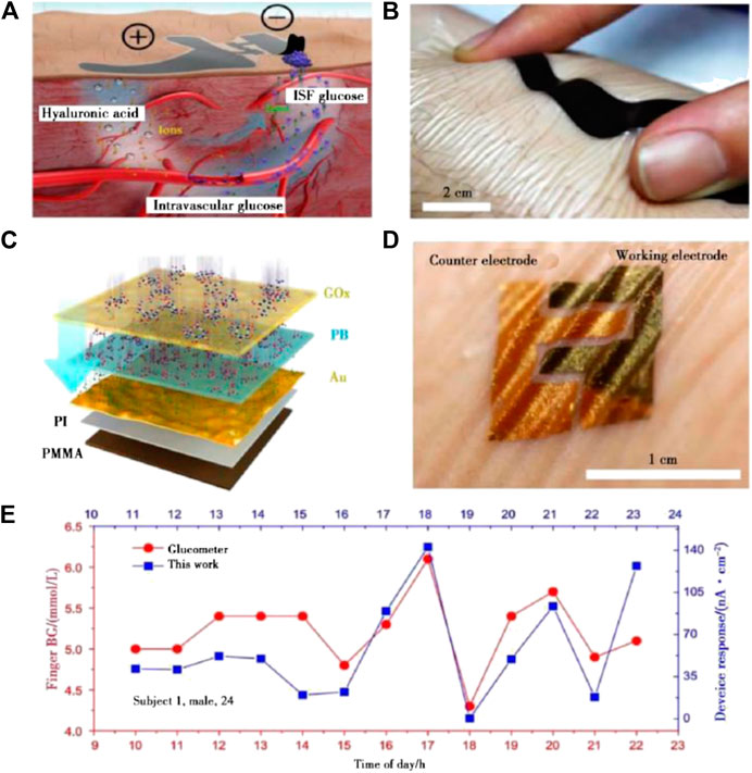
FIGURE 10. (A) Scheme of the ETCs; (B) the paper battery attached to the skin surface; (C) scheme of the skin-like biosensor multilayers; (D) the biosensor completely conforms to the skin surface; (E) results of hourly glucose monitoring in 1-day period by using a glucometer (red) and skin-like biosensor (blue) (Chen et al., 2017). Reproduced with permission.
Long-term exercise can result in inflammation and cause damage to the wrist and knee joints of the human body. The wearable flexible temperature sensor can determine whether inflammation occurs by monitoring the changes in body temperature at the joints in real time. A temperature sensor integrated on a rigid programmable polymer substrate can achieve stable measurement of body temperature at the joint. The temperature change measured by the sensor in a static state is small (0.01–0.07°C), and even during the cyclic movement, the temperature change measured is still less than 0.1°C. The change in body temperature is greater than 1°C when joint damage or inflammation occurs, which ensures that the temperature sensor can monitor joint damage (Cao et al., 2018).
The electrical potential on the surface of the heart is important in the treatment of many diseases. Signal acquisition depends on the close connection between the sensor and tissue cells, so traditional rigid detectors cannot detect the potential inside the heart. A multifunctional balloon catheter system with serpentine interconnects structure (Kim et al., 2012) includes two parts: contact sensors and multi-electrodes. High electrode density on the balloon catheter can ensure complete signal acquisition from the whole heart. This new technology enables monitoring of heart activity while causing little harm.
Biomaterials have good biocompatibility and have been widely used as substrate materials in flexible electronics. A flexible mesh electrode with silk protein as a substrate has been attached to a cat’s brain to collect brain signals (Kim et al., 2010); when the protein is dissolved by the body fluid, electrode attaches closely to the brain tissue due to capillary action. The mesh brain electrode can complete real-time scanning of the brains of cats. These devices provide options for treatment of brain diseases and realization of brain-computer interconnections.
Flexible Electronic Skin
Skin is an extremely complex sensing system that can sense external signals such as temperature and pressure, and has an important function in the interaction between humans and the environment. Electronic skin that mimics the skin function has realized the skin’s sensory function (Kaltenbrunner et al., 2013; Wang X. et al., 2015; Chortos et al., 2016). An electronic skin that includes several types of sensor can detect and conduct a variety of signals and has shown a wide range of application prospects in flexible wear, medical monitors (Kim et al., 2019) and intelligent robots (Lai et al., 2018).
One electronic skin integrates stress sensors, temperature sensors and electrical-signal detectors. This flexible electronic skin system can also further integrate transistors and radio-frequency induction coils, thereby realizing physiological signal monitoring, signal adjustment and wireless charging functions. The discomfort brought by electronic skin to the skin can be eliminated by optimizing the mechanical properties, so optimized electronic skin can be attached to a newborn's skin for intensive care (Figure 11) (Chung et al., 2019).
Real-time monitoring on the temperature and pressure changes of the prosthesis and skin interface is very important for amputation patients. An electronic skin system that can continuously measure physiological signals at the skin and prosthetic interface is prepared. This system includes three parts: a flexible integrated sensor, a wireless receiving module, and an independent display device (such as a mobile phone or a tablet). The pressure sensor adopts a three-dimensional structure design and can be integrated into a wireless platform with a built-in temperature sensor. The wireless receiving module provides wireless power to the sensor. This special electronic skin system eliminates the dependence of sensor on the power supply, and realizes the wireless connection with standard consumer electronic products. This system can measure the temperature and pressure of the prosthesis and skin interface of amputee patients under the conditions of standing, sitting and walking, and has the advantages of small hysteresis and high linearity (Kwak et al., 2020).
Biocompatibility (including compatibility in mechanics, physics and chemistry) must be considered when electronic skin is to be used for a long time. From a mechanical point of view, electronic skin cannot cause discomfort to the skin; from a physical point of view, electronic skin must have suitable air permeability to prevent liquid accumulation on the body surface; from a chemical point of view, electronic skin cannot cause skin allergic reactions. A semi-permeable membrane is has selective permeability, and can therefore block large molecules but can pass small molecules. An electronic skin containing a commercial semi-permeable membrane has been used to test body temperature (Chen et al., 2015), this electronic skin has five components: encapsulation layer, adhesive layer, functional layer, base layer and adhesion layer. Serpentine interconnects are used in the functional layer, and the base layer and encapsulation layer are made of commercial semipermeable membranes; due to its outstanding properties, the semi-permeable membrane can prevent external contaminants while allowing perspiration escape as a vapor.
Electronic skin also has application prospects in intelligent robots. As proof of concept, an artificial tactile nerve has been used to control movement of a cockroach (Kim et al., 2018). The artificial nerve is mainly composed of a pressure sensor that is mainly used to collect external pressure; a ring oscillator that can convert the pressure signal to an electric signal; and synaptic transistors that can integrate electrical signals and generate action potentials. The artificial nerve can convert the pressure signal from the pressure sensor to an oscillating signal, which can activate the muscles of the cockroach’s legs. This work provides inspiration for development of sensitive intelligent robots.
Summary and Outlook
This review has considered materials and processes used to manufacture of flexible electronic devices. Organic materials have been widely used in flexible electronics because of their excellent inherent flexibility, compatibility with flexible substrates and simple manufacturing processes. Although the electrical properties of organic materials can be improved by simple chemical modification, the stability and electrical properties of electronic devices that use on organic materials must be further improved. Rational structural design has been used to apply rigid inorganic materials in various stretchable and flexible electronics. Buckled Nanoribbons, Island-Interconnect design, Serpentine-Interconnect design, and other designs are typical inorganic electronic structures. In the past ten years of development, the stretchability of inorganic electronics has been increased from 30% to 300%. Flexible electronics is an interdisciplinary subject, including electronics, materials science and mechanics and other fields. Future research directions should seek ductile composite materials with excellent electrical properties and high stability, and develop corresponding method to processing flexible electronic devices.
Flexible electronics will improve the level of medical care and even change the existing medical model. Bio-integrated flexible sensors and electronic skin can monitor the physiological signals of the heart and brain in real time; at the same time, flexible electronic devices can integrate communication equipment and drug delivery devices to achieve intelligent drug delivery treatment. However, most of the flexible electronic devices including medical flexible electronics are in the laboratory stage. We believe that development of technology and increase in used demand for flexible electronic equipment will accelerate the process from laboratory to industrialization.
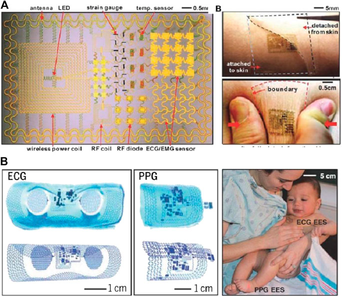
FIGURE 11. (A) Multifunctional electronics with physical properties matched to the epidermis. (B) Wireless multifunctional epidermal electronic systems for neonatal intensive care (Chung et al., 2019). Reproduced with permission.
Author Contributions
WX is the corresponding author of this article, he provided help in article writing and grammar modification; ZW is the first author of this article, and he has completed the writing of the paper article; YN, LS and LL provided assistance in language writing and article structure.
Funding
This work was supported by Guangdong Key R&D Project No. 2018B030338001, the Tianjin Science Foundation for Distinguished Young Scholars (19JCJQJC61000), the Fundamental Research Funds for the Central Universities (075-63191740, 075-63191745, 075-92022027), Hundred Young Academic Leaders Program of Nankai University (2122018218), Natural Science Foundation of Tianjin (18JCYBJC16000), the 111 Project (B16027), the International Cooperation Base (2016D01025), and Tianjin International Joint Research and Development Center.
Conflict of Interest
The authors declare that the research was conducted in the absence of any commercial or financial relationships that could be construed as a potential conflict of interest.
References
Amjadi, M., Pichitpajongkit, A., Lee, S., Ryu, S., and Park, I. (2014). Highly stretchable and sensitive strain sensor based on silver nanowire-elastomer nanocomposite. ACS Nano 8, 5154–5163. doi:10.1021/nn501204t
Arias, A. C., Daniel, J., Sambandan, S., Ng, T. N., Russo, B., Krusor, B., et al. (2008). All printed thin film transistors for flexible electronics, 7054. Washington, DC: International Society for Optics and Photonics, 70540L.
Baca, A. J., Ahn, J. H., Sun, Y., Meitl, M. A., Menard, E., Kim, H. S., et al. (2008). Semiconductor wires and ribbons for high-performance flexible electronics. Angew Chem. Int. Ed. Engl. 47, 5524–5542. doi:10.1002/anie.200703238
Bae, I., Hwang, S. K., Kim, R. H., Kang, S. J., and Park, C. (2013). Wafer-scale arrays of nonvolatile polymer memories with microprinted semiconducting small molecule/polymer blends. ACS Appl. Mater. Interfaces 5, 10696–10704. doi:10.1021/am402852y
Basaran, O. A. (2002). Small-scale free surface flows with breakup: drop formation and emerging applications. AIChE J. 48, 1842. doi:10.1002/aic.690480902
Boutry, C. M., Nguyen, A., Lawal, Q. O., Chortos, A., Rondeau-Gagné, S., and Bao, Z. (2015). A sensitive and biodegradable pressure sensor array for cardiovascular monitoring. Adv Mater Weinheim 27, 6954–6961. doi:10.1002/adma.201502535
Brosteaux, D., Fabrice Axisa, F., Gonzalez, M., and Vanfleteren, J. (2007). Design and fabrication of elastic interconnections for stretchable electronic circuits. IEEE Electron. Device Lett. 28, 552–554. doi:10.1109/led.2007.897887
Cao, Y., Zhang, G., Zhang, Y., Yue, M., Chen, Y., Cai, S., et al. (2018). Direct fabrication of stretchable electronics on a polymer substrate with process‐integrated programmable rigidity. Adv. Funct. Mater. 28, 1804604. doi:10.1002/adfm.201804604
Chang, J. W., Wang, C. G., Huang, C. Y., Tsai, T. D., Guo, T. F., and Wen, T. C. (2011). Chicken albumen dielectrics in organic field-effect transistors. Adv Mater Weinheim 23, 4077–4081. doi:10.1002/adma.201102124
Chang, W.-Y., Fang, T.-H., Lin, H.-J., Shen, Y.-T., and Lin, Y.-C. (2009). A large area flexible array sensors using screen printing technology. J. Disp. Technol. 5, 178–183. doi:10.1109/jdt.2008.2004862
Chen, Y., Lu, B., Chen, Y., and Feng, X. (2015). Breathable and stretchable temperature sensors inspired by skin. Sci. Rep. 5, 11505. doi:10.1038/srep11505
Chen, Y., Lu, S., Zhang, S., Li, Y., Qu, Z., Chen, Y., et al. (2017). Skin-like biosensor system via electrochemical channels for noninvasive blood glucose monitoring. Sci. Adv. 3, e1701629. doi:10.1126/sciadv.1701629
Chen, Z., Ren, W., Gao, L., Liu, B., Pei, S., and Cheng, H. M. (2011). Three-dimensional flexible and conductive interconnected graphene networks grown by chemical vapour deposition. Nat. Mater. 10, 424–428. doi:10.1038/nmat3001
Chortos, A., Liu, J., and Bao, Z. (2016). Pursuing prosthetic electronic skin. Nat. Mater. 15, 937–950. doi:10.1038/nmat4671
Chung, H. U., Kim, B. H., Lee, J. Y., Lee, J., Xie, Z., Ibler, E. M., et al. (2019). Binodal, wireless epidermal electronic systems with in-sensor analytics for neonatal intensive care. Science 363. doi:10.1126/science.aau0780
Chung, H. U., Rwei, A. Y., Hourlier-Fargette, A., Xu, S., Lee, K., Dunne, E. C., et al. (2020). Skin-interfaced biosensors for advanced wireless physiological monitoring in neonatal and pediatric intensive-care units. Nat. Med. 26, 418–429. doi:10.1038/s41591-020-0792-9
Dadvand, A., Sun, W.-H., Moiseev, A. G., Bélanger-Gariépy, F., Rosei, F., Meng, H., et al. (2013). 1,5-, 2,6- and 9,10-distyrylanthracenes as luminescent organic semiconductors. J. Mater. Chem. C 1, 2817–2825. doi:10.1039/c3tc30247d
Dearden, A. L., Smith, P. J., Shin, D.-Y., Reis, N., Derby, B., and O'Brien, P. (2005). A low curing temperature silver ink for use in ink-jet printing and subsequent production of conductive tracks. Macromol. Rapid Commun. 26, 315–318. doi:10.1002/marc.200400445
Deganello, D., Cherry, J., Gethin, D., and Claypole, T. (2010). Patterning of micro-scale conductive networks using reel-to-reel flexographic printing. Thin Sol. Fil., 518, 6113–6116. doi:10.1016/j.tsf.2010.05.125
Dodabalapur, A. (2006). Organic and polymer transistors for electronics. Materials Off., 9, 24–30. doi:10.1016/S1369-7021(06)71444-4
Dong, X., Chen, L., Su, X., Wang, Y., and Xia, Y. (2016). Flexible aqueous lithium-ion battery with high safety and large volumetric energy density. Angew Chem. Int. Ed. Engl. 55, 7474–7477. doi:10.1002/anie.201602766
Ershad, F., Sim, K., Thukral, A., Zhang, Y. S., and Yu, C. (2019). Invited Article: emerging soft bioelectronics for cardiac health diagnosis and treatment. Apl. Mater. 7, 031301. doi:10.1063/1.5060270
Feng, W., Zheng, W., Gao, F., Chen, X., Liu, G., Hasan, T., et al. (2016). Sensitive electronic-skin strain sensor array based on the patterned two-dimensional α-In2Se3. Chem. Mater. 28, 4278–4283. doi:10.1021/acs.chemmater.6b01073
Fleischhaker, F., Wloka, V., and Hennig, I. (2010). ZnO based field-effect transistors (FETs): solution-processable at low temperatures on flexible substrates. J. Mater. Chem. 20, 6622–6625. doi:10.1039/c0jm01477j
Forrest, S. R. (2004). The path to ubiquitous and low-cost organic electronic appliances on plastic. Nature 428, 911–918. doi:10.1038/nature02498
Gao, Z., Zhang, Y., Song, N., and Li, X. (2017). Towards flexible lithium-sulfur battery from natural cotton textile. Electrochim. Acta 246, 507–516. doi:10.1016/j.electacta.2017.06.069
Gates, B. D. (2009). Materials science: flexible electronics. Science 323, 1566–1567. doi:10.1126/science.1171230
Gonzalez, M., Axisa, F., Bulcke, M. V., Brosteaux, D., Vandevelde, B., and Vanfleteren, J. (2008). Design of metal interconnects for stretchable electronic circuits. Microelectron Reliab., 48, 825–832. doi:10.1016/j.microrel.2008.03.025
Gray, D. S., Tien, J., and Chen, C. S. (2004). High-conductivity elastomeric electronics. Adv. Mater. 16, 393–397. doi:10.1002/adma.200306107
Groenendaal, L., Jonas, F., Freitag, D., Pielartzik, H., and Reynolds, J. R. (2000). Poly(3,4-ethylenedioxythiophene) and its derivatives: past, present, and future. Adv. Mater. 12, 481–494. doi:10.1002/(sici)1521-4095(200004)12:7<481::aid-adma481>3.0.co;2-c
Hanna, J., Bteich, M., Tawk, Y., Ramadan, A. H., Dia, B., Asadallah, F. A., et al. (2020). Noninvasive, wearable, and tunable electromagnetic multisensing system for continuous glucose monitoring, mimicking vasculature anatomy. Sci Adv 6, eaba5320. doi:10.1126/sciadv.aba5320
Huang, Y., Wu, H., Xiao, L., Duan, Y., Zhu, H., Bian, J., et al. (2019). Assembly and applications of 3D conformal electronics on curvilinear surfaces. Mater. Horiz. 6, 642–683. doi:10.1039/c8mh01450g
Huyghe, B., Rogier, H., Vanfleteren, J., and Axisa, F. (2008). Design and manufacturing of stretchable high-frequency interconnects. IEEE Trans. Adv. Packag. 31, 802–808. doi:10.1109/tadvp.2008.927811
Jedaa, A., and Halik, M. (2009). Toward strain resistant flexible organic thin film transistors Appl. Phys. Lett. 95, 237. doi:10.1063/1.3216587
Jiang, H., Khang, D. Y., Song, J., Sun, Y., Huang, Y., and Rogers, J. A. (2007). Finite deformation mechanics in buckled thin films on compliant supports. Proc. Natl. Acad. Sci. USA 104, 15607–15612. doi:10.1073/pnas.0702927104
Jiang, Z., Wang, Y., Yuan, S., Shi, L., Wang, N., Xiong, J., et al. (2019). Ultrahigh-working-frequency embedded supercapacitors with 1T phase MoSe2 nanosheets for system-in-package application. Adv. Funct. Mater. 29, 1807116. doi:10.1002/adfm.201970058
Jin, Y., Chen, G., Lao, K., Li, S., Lu, Y., Gan, Y., et al. (2020). Identifying human body states by using a flexible integrated sensor npj Flex. Electron 4, 1–8. doi:10.1038/s41528-020-00090-9
Jung, S.-W., Baeg, K.-J., Yoon, S.-M., You, I.-K., Lee, J.-K., Kim, Y.-S., et al. (2010). Low-voltage-operated top-gate polymer thin-film transistors with high capacitance poly(vinylidene fluoride-trifluoroethylene)/poly(methyl methacrylate) dielectrics. J. Appl. Phys. 108, 102810. doi:10.1063/1.3511697
Jung, Y., Kline, R. J., Fischer, D. A., Lin, E. K., Heeney, M., McCulloch, I., et al. (2008). The effect of Interfacial roughness on the thin film morphology and charge transport of high-performance polythiophenes. Adv. Funct. Mater. 18, 742–750. doi:10.1002/adfm.200701089
Kaltenbrunner, M., Sekitani, T., Reeder, J., Yokota, T., Kuribara, K., Tokuhara, T., et al. (2013). An ultra-lightweight design for imperceptible plastic electronics. Nature 499, 458–463. doi:10.1038/nature12314
Kang, H., Sowade, E., and Baumann, R. R. (2014). Direct intense pulsed light sintering of inkjet-printed copper oxide layers within six milliseconds. ACS Appl. Mater. Interfaces 6, 1682–1687. doi:10.1021/am404581b
Khang, D-Y., Jiang, H., Huang, Y., and Rogers, J. A. (2006). A stretchable form of single-crystal silicon for high-performance electronics on rubber substrates. Science 311, 208–212. doi:10.1126/science.1121401
Khang, D.-Y., Rogers, J. A., and Lee, H. H. (2009). Mechanical buckling: mechanics, metrology, and stretchable electronics. Adv. Funct. Mater. 19, 1526–1536. doi:10.1002/adfm.200801065
Kim, D.-H., Ahn, J.-H., Choi, W. M., Kim, H-S., Kim, T-H., Song, J., et al. (2008a). Stretchable and foldable silicon integrated circuits. Science 320, 507–511. doi:10.1126/science.1154367
Kim, D. H., Ghaffari, R., Lu, N., Wang, S., Lee, S. P., Keum, H., et al. (2012). Electronic sensor and actuator webs for large-area complex geometry cardiac mapping and therapy. Proc. Natl. Acad. Sci. U.S.A. 109, 19910–19915. doi:10.1073/pnas.1205923109
Kim, D. H., Song, J., Choi, W. M., Kim, H. S., Kim, R. H., Liu, Z., et al. (2008b). Materials and noncoplanar mesh designs for integrated circuits with linear elastic responses to extreme mechanical deformations. Proc. Natl. Acad. Sci. U.S.A. 105, 18675–18680. doi:10.1073/pnas.0807476105
Kim, D. H., Viventi, J., Amsden, J. J., Xiao, J., Vigeland, L., Kim, Y. S., et al. (2010). Dissolvable films of silk fibroin for ultrathin conformal bio-integrated electronics. Nat. Mater. 9, 511–517. doi:10.1038/nmat2745
Kim, D. H., and Rogers, J. A. (2008). Stretchable electronics: materials strategies and devices. Adv. Mater. 20, 4887–4892. doi:10.1002/adma.200801788
Kim, J., Campbell, A. S., de Ávila, B. E., and Wang, J. (2019). Wearable biosensors for healthcare monitoring. Nat. Biotechnol. 37, 389–406. doi:10.1038/s41587-019-0045-y
Kim, Y., Chortos, A., Xu, W., Liu, Y., Oh, J. Y., Son, D., et al. (2018). A bioinspired flexible organic artificial afferent nerve. Science 360, 998–1003. doi:10.1126/science.aao0098
King, B. H., and Ramahi, D. H. (2009). Aerosol Jet (R) printing system for photovoltaic applications. Google Patents. doi:10.1109/pvsc.2009.5411213
Ko, H. C., Shin, G., Wang, S., Stoykovich, M. P., Lee, J. W., Kim, D. H., et al. (2009). Curvilinear electronics formed using silicon membrane circuits and elastomeric transfer elements. Small, 5, 2703–2709. doi:10.1002/smll.200900934
Kordás, K., Mustonen, T., Tóth, G., Jantunen, H., Lajunen, M., Soldano, C., et al. (2006). Inkjet printing of electrically conductive patterns of carbon nanotubes. Small 2, 1021–1025.
Kwak, J. W., Han, M., Xie, Z., Chung, H. U., Lee, J. Y., Avila, R., et al. (2020). Wireless sensors for continuous, multimodal measurements at the skin interface with lower limb prostheses. Sci. Transl. Med. 12. doi:10.1126/scitranslmed.abc4327
Kwon, H., Choi, W., Lee, D., Lee, Y., Kwon, J., Yoo, B., et al. (2014). Selective and localized laser annealing effect for high-performance flexible multilayer MoS2 thin-film transistors. Nano Res. 7, 1137. doi:10.1007/s12274-014-0476-1
Kwon, Y. H., Woo, S. W., Jung, H. R., Yu, H. K., Kim, K., Oh, B. H., et al. (2012). Cable-type flexible lithium ion battery based on hollow multi-helix electrodes. Adv. Mater Weinheim. 24, 5192–5145. doi:10.1002/adma.201202196
Lai, Y.-C., Deng, J., Liu, R., Hsiao, Y.-C., Zhang, S. L., Peng, W., et al. (2018). Actively perceiving and responsive soft robots enabled by self-powered, highly extensible, and highly sensitive triboelectric proximity- and pressure-sensing skins. Adv. Mater. 30, 1801114. doi:10.1002/adma.201801114
Le, H. P. (1998). Progress and trends in ink-jet printing technology. J. Imag. Sci. Technol. 42 (1), 49–62.
Lee, J., Wu, J., Shi, M., Yoon, J., Park, S. I., Li, M., et al. (2011). Stretchable GaAs photovoltaics with designs that enable high areal coverage. Adv Mater Weinheim 23, 986–991. doi:10.1002/adma.201003961
Lee, P., Lee, J., Lee, H., Yeo, J., Hong, S., Nam, K. H., et al. (2012). Highly stretchable and highly conductive metal electrode by very long metal nanowire percolation network. Adv Mater Weinheim 24, 3326–3332. doi:10.1002/adma.201200359
Lee, S. K., Jang, H. Y., Jang, S., Choi, E., Hong, B. H., Lee, J., et al. (2012). All graphene-based thin film transistors on flexible plastic substrates. Nano Lett. 12, 3472–3476. doi:10.1021/nl300948c
Li, H., Ma, Y., and Huang, Y. (2020). Material innovation and mechanics design for substrates and encapsulation of flexible electronics: a review Mater. Horizons. doi:10.1039/d0mh00483a
Li, J., Zhou, K., Liu, J., Zhen, Y., Liu, L., Zhang, J., et al. (2017). Aromatic extension at 2,6-positions of anthracene toward an elegant strategy for organic semiconductors with efficient charge transport and strong solid state emission. J. Am. Chem. Soc. 139, 17261–17264. doi:10.1021/jacs.7b09381
Li, T., Luo, H., Qin, L., Wang, X., Xiong, Z., Ding, H., et al. (2016). Flexible capacitive tactile sensor based on micropatterned dielectric layer. Small 12, 5042–5048. doi:10.1002/smll.201600760
Linghu, C., Zhang, S., Wang, C., and Song, J. (2018). Transfer printing techniques for flexible and stretchable inorganic electronics npj Flex. Electron 2, 1–14. doi:10.1038/s41528-018-0037-x
Lipomi, D. J., Vosgueritchian, M., Tee, B. C., Hellstrom, S. L., Lee, J. A., Fox, C. H., et al. (2011). Skin-like pressure and strain sensors based on transparent elastic films of carbon nanotubes. Nat. Nanotechnol. 6, 788–792. doi:10.1038/nnano.2011.184
Liu, Y., He, K., Chen, G., Leow, W. R., and Chen, X. (2017). Nature-inspired structural materials for flexible electronic devices. Chem. Rev. 117, 12893–12941. doi:10.1021/acs.chemrev.7b00291
Long, Y. Z., Yu, M., Sun, B., Gu, C. Z., and Fan, Z. (2012). Recent advances in large-scale assembly of semiconducting inorganic nanowires and nanofibers for electronics, sensors and photovoltaics. Chem. Soc. Rev. 41, 4560–4580. doi:10.1039/c2cs15335a
Ma, Y., Zhang, Y., Cai, S., Han, Z., Liu, X., Wang, F., et al. (2020). Flexible hybrid electronics for digital healthcare. Adv. Mater. 32, 1902062. doi:10.1002/adma.201902062
Madhvapathy, S. R., Wang, H., Kong, J., Zhang, M., Lee, J. Y., Park, J. B., et al. (2020). Reliable, low-cost, fully integrated hydration sensors for monitoring and diagnosis of inflammatory skin diseases in any environment. Sci. Adv. 6. doi:10.1126/sciadv.abd7146
Meitl, M. A., Zhu, Z.-T., Kumar, V., Lee, K. J., Feng, X., Huang, Y. Y., et al. (2006). Transfer printing by kinetic control of adhesion to an elastomeric stamp. Nat. Mater. 5, 33–38. doi:10.1038/nmat1532
Nambiar, S., and Yeow, J. T. (2011). Conductive polymer-based sensors for biomedical applications. Biosens. Bioelectron. 26, 1825–1832. doi:10.1016/j.bios.2010.09.046
Nathan, A., Ahnood, A., Cole, M. T., Lee, S., Suzuki, Y., Hiralal, P., et al. (2012). Flexible electronics: the next ubiquitous platform. Proc. IEEE 100, 1486–1517. doi:10.1109/JPROC.2012.2190168
Öhlund, T., Schuppert, A. K., Hummelgard, M., Bäckström, J., Nilsson, H-E., and Olin, H. k. (2015). Inkjet fabrication of copper patterns for flexible electronics: using paper with active precoatings. ACS Appl. Mater. Interfaces 7, 18273–18282. doi:10.1021/acsami.5b03061
Pal, R. K., Pradhan, S., Narayanan, L., and Yadavalli, V. K. (2018). Micropatterned conductive polymer biosensors on flexible PDMS films. Sensor. Actuator. B Chem. 259, 498–504. doi:10.1016/j.snb.2017.12.082
Park, J., Wang, S., Li, M., Ahn, C., Hyun, J. K., Kim, D. S., et al. (2012). Three-dimensional nanonetworks for giant stretchability in dielectrics and conductors. Nat. Commun. 3, 916–918. doi:10.1038/ncomms1929
Park, J. U., Hardy, M., Kang, S. J., Barton, K., Adair, K., Mukhopadhyay, D. K., et al. (2007). High-resolution electrohydrodynamic jet printing. Nat. Mater. 6, 782–789. doi:10.1038/nmat1974
Pelrine, R., Kornbluh, R., Pei, Q., and Joseph, J. (2000). High-speed electrically actuated elastomers with strain greater than 100%. Science 287, 836–839. doi:10.1126/science.287.5454.836
Phan, H. D., Kim, Y., Lee, J., Liu, R., Choi, Y., Cho, J. H., et al. (2017). Ultraclean and direct transfer of a wafer-scale MoS2 thin film onto a plastic substrate. Adv. Mater. 29, 1603928. doi:10.1002/adma.201603928
Pu, X., Li, L., Song, H., Du, C., Zhao, Z., Jiang, C., et al. (2015). A self-charging power unit by integration of a textile triboelectric nanogenerator and a flexible lithium-ion battery for wearable electronics. Adv Mater Weinheim 27, 2472–2478. doi:10.1002/adma.201500311
Ray, T. R., Choi, J., Bandodkar, A. J., Krishnan, S., Gutruf, P., Tian, L., et al. (2019). Bio-integrated wearable systems: a comprehensive review. Chem. Rev. 119, 5461–5533. doi:10.1021/acs.chemrev.8b00573
Reitberger, T., Hoerber, J., Schramm, R., Sennefelder, S., and Franke, J. (2015). Aerosol Jet printing of optical waveguides. Piscataway, NJ: IEEE, 5–10.
Rogers, J. A., Someya, T., and Huang, Y. (2010). Materials and mechanics for stretchable electronics. Science 327, 1603–1607. doi:10.1126/science.1182383
Sandström, A., Dam, H. F., Krebs, F. C., and Edman, L. (2012). Ambient fabrication of flexible and large-area organic light-emitting devices using slot-die coating. Nat. Commun. 3, 1002–1005. doi:10.1038/ncomms2002
Schwartz, G., Tee, B. C., Mei, J., Appleton, A. L., Kim, D. H., Wang, H., et al. (2013). Flexible polymer transistors with high pressure sensitivity for application in electronic skin and health monitoring. Nat. Commun. 4, 1859. doi:10.1038/ncomms2832
Seng, K. H., Liu, J., Guo, Z. P., Chen, Z. X., Jia, D., and Liu, H. K. (2011). Free-standing V2O5 electrode for flexible lithium ion batteries. Electrochem. Commun. 13 (5), 383–386. doi:10.1016/j.elecom.2010.12.002
Shen, G., and Fan, Z. (2016). Flexible electronics: from materials to devices. Singapore: World Scientific Publishing.
Shen, W., Zhang, X., Huang, Q., Xu, Q., and Song, W. (2014). Preparation of solid silver nanoparticles for inkjet printed flexible electronics with high conductivity. Nanoscale 6, 1622–1628. doi:10.1039/c3nr05479a
Shirakawa, H., McDiarmid, A., and Heeger, A. (2003). Twenty-five years of conducting polymers. Chem. Comm 7, 1–4.
Sirringhaus, H., Kawase, T., Friend, R., Shimoda, T., Inbasekaran, M., Wu, W., et al. (2000). High-resolution inkjet printing of all-polymer transistor circuits. Science 290 (5499), 2123–2126. doi:10.1126/science.290.5499.2123
Someya, T., Kato, Y., Sekitani, T., Iba, S., Noguchi, Y., Murase, Y., et al. (2005). Conformable, flexible, large-area networks of pressure and thermal sensors with organic transistor active matrixes. Proc. Natl. Acad. Sci. U.S.A. 102, 12321–12325. doi:10.1073/pnas.0502392102
Song, J., Feng, X., and Huang, Y. (2016). Mechanics and thermal management of stretchable inorganic electronics. Natl. Sci. Rev. 3, 128–143. doi:10.1093/nsr/nwv078
Song, J., Jiang, H., Huang, Y., and Rogers, J. A. (2009). Mechanics of stretchable inorganic electronic materials. J. Vac. Sci. Technol.: Vacuum, Surfaces, and Films 27, 1107–1125. doi:10.1116/1.3168555
Su, Y., Ping, X., Yu, K. J., Lee, J. W., Fan, J. A., Wang, B., et al. (2017). In-plane deformation mechanics for highly stretchable electronics. Adv. Mater. 29, 1604989. doi:10.1002/adma.201604989
Sun, Q., Fang, X., Weng, W., Deng, J., Chen, P., Ren, J., et al. (2017). An aligned and laminated nanostructured carbon hybrid cathode for high-performance lithium-sulfur batteries. Angew. Chem. 127, 10685–10690. doi:10.1002/ange.201504514
Sun, T., Tasnim, F., McIntosh, R. T., Amiri, N., Solav, D., Anbarani, M. T., et al. (2020). Decoding of facial strains via conformable piezoelectric interfaces. Nat. Biomed. Eng. 4, 954–972. doi:10.1038/s41551-020-00612-w
Sun, Y., Choi, W. M., Jiang, H., Huang, Y. Y., and Rogers, J. A. (2006). Controlled buckling of semiconductor nanoribbons for stretchable electronics. Nat. Nanotechnol. 1, 201–207. doi:10.1038/nnano.2006.131
Sun, Y., and Rogers, J. A. (2007). Structural forms of single crystal semiconductor nanoribbons for high-performance stretchable electronics. J. Mater. Chem. 17, 832–840. doi:10.1039/b614793c
Trung, T. Q., and Lee, N.-E. (2017). Recent progress on stretchable electronic devices with intrinsically stretchable components. Adv. Mater. 29, 1603167. doi:10.1002/adma.201603167
Wan, Y., Qiu, Z., Hong, Y., Wang, Y., Zhang, J., Liu, Q., et al. (2018). A highly sensitive flexible capacitive tactile sensor with sparse and high-aspect-ratio microstructures. Adv. Electron. Mater. 4, 1700586. doi:10.1002/aelm.201700586
Wang, B., Bao, S., Vinnikova, S., Ghanta, P., and Wang, S. (2017). Buckling analysis in stretchable electronics npj Flex. Electron 1, 1–9. doi:10.1038/s41528-017-0004-y
Wang, C., Wang, X., Yang, Y., Kushima, A., Chen, J., Huang, Y., et al. (2015). Slurryless Li2S/reduced graphene oxide cathode paper for high-performance lithium sulfur battery. Nano Lett. 15, 1796–1802. doi:10.1021/acs.nanolett.5b00112
Wang, S., Huang, Y., and Rogers, J. A. (2015). Mechanical designs for inorganic stretchable circuits in soft electronics. IEEE Trans. Compon. Packag. Manuf. Technol. 5, 1201–1218. doi:10.1109/TCPMT.2015.2417801
Wang, X., Dong, L., Zhang, H., Yu, R., Pan, C., and Wang, Z. L. (2015). Recent progress in electronic skin. Adv. Sci. 2, 1500169. doi:10.1002/advs.201500169
Wang, Z., Cheng, J., Guan, Q., Huang, H., Li, Y., Zhou, J., et al. (2018). All-in-one fiber for stretchable fiber-shaped tandem supercapacitors. Nanomater. Energy 45, 210–219. doi:10.1016/j.nanoen.2017.12.054
Wei, T., Ruan, J., Fan, Z., Luo, G., and Wei, F. (2007). Preparation of a carbon nanotube film by ink-jet printing. Carbon 45 (13), 2712–2716. doi:10.1016/j.carbon.2007.08.009
Wong, R. D. P., Posner, J. D., and Santos, V. J. (2012). Flexible microfluidic normal force sensor skin for tactile feedback Sensor. Actual. A-Phys 179, 62–69. doi:10.1016/j.sna.2012.03.023
Wong, W. S., Chabinyc, M. L., Ng, T-N., and Salleo, A. (2009). Flexible electronics. Berlin, Germany: Springer, 143–181.
Woo, K., Kim, D., Kim, J. S., Lim, S., and Moon, J. (2009). Ink-jet printing of cu-ag-based highly conductive tracks on a transparent substrate. Langmuir 25, 429–433. doi:10.1021/la802182y
Xu, J., Wang, S., Wang, G. N., Zhu, C., Luo, S., Jin, L., et al. (2017). Highly stretchable polymer semiconductor films through the nanoconfinement effect. Science 355, 59–64. doi:10.1126/science.aah4496
Yang, C. C., and Li, S. (2007). Investigation of cohesive energy effects on size-dependent physical and chemical properties of nanocrystals. Phys. Rev. B 75, 165413. doi:10.1103/physrevb.75.165413
Yao, Y., Dong, H., and Hu, W. (2016). Charge transport in organic and polymeric semiconductors for flexible and stretchable devices. Adv Mater Weinheim 28, 4513–4523. doi:10.1002/adma.201503007
Yoon, J., Zhang, Z., Lu, N., and Suo, Z. (2007). The effect of coating in increasing the critical size of islands on a compliant substrate. Appl. Phys. Lett. 90, 211912. doi:10.1063/1.2742911
Zhang, Y., Fu, H., Xu, S., Fan, J. A., Hwang, K.-C., Jiang, J., et al. (2014a). A hierarchical computational model for stretchable interconnects with fractal-inspired designs. J. Mech. Phys. Solid. 72, 115–130. doi:10.1016/j.jmps.2014.07.011
Zhang, Y., Wang, S., Li, X., Fan, J. A., Xu, S., Song, Y. M., et al. (2014b). Experimental and theoretical studies of serpentine microstructures bonded to prestrained elastomers for stretchable electronics. Adv. Funct. Mater. 24, 2028–2037. doi:10.1002/adfm.201302957
Zheng, L., Qiu, Z., You, Y., Liu, Z., and Liu, R. (2014). Flexible large area printed electronics for the internet of things applications. Mat. China, 33, 135–143. doi:10.7502/j.issn.1674-3962.2014.03.02
Zheng, N., Huang, Y., Zhao, Q., Feng, X., and Xie, T. (2016). Shape memory polymers for flexible electronics SCIENTIA SINICA Physica. Mech. Astrono. 46, 044602.
Keywords: flexible electronics, structural design, flexible material, stretchability, medical applications
Citation: Wang Z, Sun L, Ni Y, Liu L and Xu W (2021) Flexible Electronics and Healthcare Applications. Front. Nanotechnol. 3:625989. doi: 10.3389/fnano.2021.625989
Received: 04 November 2020; Accepted: 06 January 2021;
Published: 18 March 2021.
Edited by:
Xian Huang, Tianjin University, ChinaCopyright © 2021 Wang, Sun, Ni, Liu and Xu. This is an open-access article distributed under the terms of the Creative Commons Attribution License (CC BY). The use, distribution or reproduction in other forums is permitted, provided the original author(s) and the copyright owner(s) are credited and that the original publication in this journal is cited, in accordance with accepted academic practice. No use, distribution or reproduction is permitted which does not comply with these terms.
*Correspondence: Wentao Xu, d2VudGFvQG5hbmthaS5lZHUuY24=Ym51Y2hAaG90bWFpbC5jb20=