 Keyuan Ding
 Tianci Li
 Feng Rao
- College of Materials Science and Engineering, Shenzhen University, Shenzhen, China
Extending cycling endurance and suppressing programming noise of phase-change random-access memory (PCRAM) are the key challenges with respect to the development of nonvolatile working memory and high-accuracy neuromorphic computing devices. However, the large-scale atomic migration along electrical pulse direction in the unconstrained three-dimensional phase transitions of the phase-change materials (PCMs) induces big resistance fluctuations upon repeated programming and renders the classic PCRAM devices into premature failure with limited cycling endurance. Previous efforts of superlattice-like and superlattice PCM schemes cannot effectively resolve such issues. In this work, we demonstrated that, through fine-tuning the sputtering techniques, a phase-change heterostructure (PCH) of Sb2Te3/TiTe2 can be successfully constructed. In contrast to its superlattice-like counterpart with inferior crystal quality, the well-textured PCH architecture ensures the reliable (well-confined) two-dimensional phase transitions, promoting an ultralow-noise and long-life operation of the PCRAM devices. Our study thus provides a useful reference for better manufacturing the PCH architecture and further exploring the excellent device performances and other new physics.
Introduction
With the development of the Internet of Things, the exponentially growing demands in data processing and storage have imposed critical requirements on the energy efficiency and computing speed for data-centric tasks. But in the current computing system based on classic von Neumann architecture, the constant data shuttling between a fast central processing unit (CPU) and other much slower program and storage memory units leads to significantly wasted working power and limited computing speed (Kestor et al., 2013; Wong and Salahuddin, 2015). Extensive studies on phase-change random-access memory (PCRAM) (Wuttig, 2005; Raoux et al., 2010) thus have been devoted to resolving the issues. One route is to renovate the von Neumann architecture by alleviating performance mismatch among hierarchical memories (Lam, 2010; Rao et al., 2015; Yu and Chen, 2016; Rao et al., 2017), such as Intel’s Optane DC (Choe, 2017) chips bridged between volatile dynamic random-access memory (DRAM) and nonvolatile solid-state drive (SSD) flash memory. The other is to innovate non-von Neumann architecture by unifying processing with storage in PCRAM cells, such as neuromorphic computing of three paradigms (Kuzum et al., 2012; Tuma et al., 2016; Burr et al., 2017; Boybat et al., 2018; Ielmini and Wong, 2018; Le Gallo et al., 2018; Sebastian et al., 2018): in-memory computing, deep neural networks, and spiking neural networks.
Commercialized PCRAM device encodes digital information through reversible transformation between amorphous and crystalline phases of chalcogenide PCMs (Chen et al., 2019; Rao et al., 2019), e.g., Ge2Sb2Te5 (GST). Typical (mushroom- or pillar-type) PCRAM devices execute three-dimensional (3D) phase transitions of GST film, where extensive cycles of high-energy/high-bias RESET (melting and amorphization) operation pulses trigger long-distance migrations of Sb (Ge) and Te elements in opposite (vertical) directions (Padilla et al., 2010; Xie et al., 2018), giving rise to the phase segregation and the formation of large voids near the bottom electrode. This degrades the performing reliability and limits the endurance of mass-produced GST devices to ∼109–1012 cycles (Yu and Chen, 2016; Xie et al., 2018), obstructing the implementation of PCRAM as nonvolatile working memory (with > ∼1016 cycles) for the deep modification of the von Neumann architecture (Wong and Salahuddin, 2015). Such a considerable deviation/variation in composition and microstructure during the unconstrained 3D phase transitions generates large fluctuations (noises) in programming resistance states, which poses crucial challenges to the accomplishments of high-accuracy and high-efficiency matrix-vector multiplications, unsupervised learning of temporal patterns, and other data-centric computational tasks (Burr et al., 2017; Sebastian et al., 2018).
Many efforts, e.g., superlattice-like (SLL) (Chong et al., 2006; Lu et al., 2012; Chia Tan et al., 2013) and superlattice (SL) (Simpson et al., 2011; Soeya et al., 2013; Takaura et al., 2014) PCM architectures, have been made to address the issue of limited endurance, attempting to tailor the 3D phase transitions into 2D fashion. However, both schemes encounter difficulties in maintaining a reliable 2D structural transformation upon repeated programming, because the RESET operations must be cautiously performed to avoid local overheating; otherwise the multilayers may melt together and then quench into a mixed amorphous phase (Simpson et al., 2011; Li et al., 2018), as the melting temperatures (Tm, being ∼900–1,000 K) of the adopted PCMs in SLL or SL architectures are quite close (Chong et al., 2006; Simpson et al., 2011; Lu et al., 2012; Chia Tan et al., 2013; Soeya et al., 2013; Takaura et al., 2014). In addition, the growth condition must be tightly controlled to construct Ge(Sn)Te/Sb2Te3 SLs as Ge(Sn)Te is chemically reactive and may alloy into Ge(Sn)SbTe-like compounds easily during synthesis (Li et al., 2018). Inspired by the previous findings, we recently proposed a distinct approach to address the above issues by an innovative PCH design using Sb2Te3/TiTe2 stackings (Ding et al., 2019). The relations between crystal quality of such stackings and the derived electrical performances have not been disclosed yet. In this work, we draw direct comparisons between Sb2Te3/TiTe2 SLL and PCH (SL) cases. Note that here we only care about the sputtering technology that is commonly employed in mass production of PCRAM chips, rather than other techniques such as molecular beam epitaxy or chemical vapor deposition. We further reveal that, in contrast to the SLL case, only the well-textured (highly oriented) PCH architecture can guarantee a reliable 2D switching to inhibit large-scale (long-distance) atomic diffusion along electrical pulse direction, enabling substantially prolonged cycling endurance and suppressed programming noise.
Experimental Section
Film Preparation and Characterization
The Sb2Te3 and TiTe2 films were deposited on a SiO2/Si substrate by sputtering the respective pure target in ultra-high vacuum with a base pressure of <∼1 × 10⁻⁸ Torr, and the deposition pressure was under ∼4.7 mTorr. For in situ heating (at ∼300°C) deposition of the Sb2Te3, TiTe2, and PCH films, the deposition rate of Sb2Te3 and TiTe2 sublayers was controlled to be ∼0.5–1.0 nm/min. A ∼5 nm thick Sb2Te3 seed layer was predeposited on the substrate before PCH film deposition. The ordinary Sb2Te3, TiTe2, and SLL films were deposited at room temperature without the seed layer, and the deposition rate of Sb2Te3 and TiTe2 sublayers was controlled to be ∼5 nm/min. The deposited Sb2Te3 and TiTe2 sublayers are ∼5 nm and ∼3 nm thick in PCH and SLL architectures. Half of the as-deposited films were postannealed at 300°C for 1 h. A ∼10 nm thick SiO2 capping layer was in situ grown on top of each film inside the vacuum chamber to avoid oxidation. The film compositions were confirmed by Axios X-ray fluorescence spectrum (PANalytical B.V. Netherlands). The surface morphology of the films was analyzed by field emission scanning electron microscope (SEM) ZEISS SUPRA 55. The X-ray diffraction (XRD) method was employed to characterize the crystal structures of the films (∼100 nm in thickness) in the 2θ range of 5–60o, using Cu/Kα radiation with a scanning step of 0.02o.
Device Fabrication and Electrical Characterization
Mushroom-type SLL- and PCH-based PCRAM devices with tungsten bottom electrode contact of ∼190 nm in diameter were fabricated using the 0.13 μm node complementary metal-oxide semiconductor technology. The thickness of the SLL and PCH films in the devices was controlled to be ∼70 nm. The ∼15 nm thick TiN and ∼300 nm thick Al films were used as top electrode in all devices. The PCH film was deposited onto the bottom electrode of the PCRAM device under ∼300°C, while SLL film in the PCRAM device was deposited at room temperature. The as-fabricated SLL-based device then was postannealed at 300°C for 1 h. All the electrical measurements on PCRAM devices were performed by using the Keithley 2400C source meter (measuring device/film resistance) and the Tektronix AWG5002B/AWG5202 pulse generator (generating voltage pulse with a minimum width of ∼6 ns).
Ab Initio Simulations
All the ab initio simulations were carried out with Vienna Ab initio Simulations Package (VASP) (Kresse and Hafner, 1993). The Perdew-Burke-Ernzerhof (PBE) functionals (Perdew et al., 1996) and the projector augmented wave (PAW) pseudopotentials (Blöchl, 1994) were used for VASP. The 233-atom hexagonal supercells of SLL and PCH architectures were simulated with periodic boundary conditions by NVT density functional theory- (DFT-) based molecular dynamics (DFMD). The energy cutoff is 180 eV and the time step is 3 femtoseconds.
Results and Discussion
Crystal Orientation and Morphology
Regarding the SLL films synthesized at room temperature, the sublayers are usually amorphous or have poor crystallinity (Chong et al., 2006; Lu et al., 2012; Chia Tan et al., 2013). Similar situation was observed for the Sb2Te3/TiTe2 SLL samples, as well as the pure Sb2Te3 and TiTe2 films grown on SiO2 substrates (Supplementary Figure S1). We employed strong postannealing actions (at 300°C for 1 h) on the as-deposited samples to promote crystallization (Figure 1A). Both the Sb2Te3 and TiTe2 films possess a hexagonal lattice configuration with multiple different (random) crystal orientations (Figure 1A), showing polycrystalline morphology with quite small grain size (< ∼20 nm) (Figures 1B,C). One can find many crystal ribbons and particles that may belong to the Ti-rich titanium tellurides precipitate from the annealed TiTe2 film (Figure 1C), which shall form rough interfaces between the sublayers inside the SLL film. It is clear that the postannealed Sb2Te3/TiTe2 SLL film inherits almost all the crystal orientations from its subunits (Figure 1A), as well as an unsmoothed surface where some crystal grains aggregated into small islands (Figure 1D).
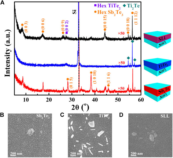
FIGURE 1. (A) XRD curves of ∼100 nm thick Sb2Te3, TiTe2, and SLL films sandwiched between SiO2 layers (see the corresponding sketch). The films were all deposited at room temperature and then postannealed at 300°C for 1 h, mainly showing the hexagonal (Hex) lattice configuration. For the sake of better observing the weak diffraction peaks, the diffraction intensity is multiplied by 50 for all the curves. (B–D) SEM images of the postannealed Sb2Te3, TiTe2, and SLL films, respectively.
In stark contrast to the inferior crystalline qualities of the as-deposited and postannealed SLL films, the diffraction intensity, crystal orientation, and surface morphology of the samples fabricated by using in situ heating (at ∼300°C) and slow growth (∼0.5–1.0 nm/min) technique (see Materials and Methods) are significantly optimized (Figure 2). A ∼5 nm thick hexagonal Sb2Te3 seed layer was pregrown on the SiO2 substrate before the film deposition (Saito et al., 2016; Zhou et al., 2016), acting as a crystallization template to assist epitaxial-like crystal growth. All the in situ heating samples have much higher diffraction intensities than those of the postannealed ones, denoting the complete crystallinity for the formers (Supplementary Figure S2). It is also worth noting that only the strong (0 0 l) diffraction peaks appear for the in situ heating Sb2Te3 sample (Figure 2A), whereas the most prominent diffraction peaks of the postannealed Sb2Te3, i.e., (0 1 5) and (1 0 10) in Figure 1A, become invisible. This identifies that the degree of c-axis orientation of Sb2Te3 crystal is greatly improved by the optimized growth technique. The in situ heating Sb2Te3 sample has quite larger hexagonal grains (>∼150–200 nm), with the (0 0 l) plane parallel to the substrate surface (Figure 2B). The in situ heating TiTe2 sample is also well oriented along c-axis (Figure 2A), exhibiting a uniform surface morphology (Figure 2C), without any big segregated crystals of non-(0 0 l) orientations. On this basis, we then alternately deposited the Sb2Te3 and TiTe2 nanolayers to construct the PCH architecture. Unsurprisingly, it also displays only the (0 0 l) diffraction peaks corresponding to the ones of its subunits (Figure 2A). Compared to the coarse granular surface of the SLL film, triangular crystals with rather bigger size (> ∼100 nm) and pretty smooth texture were formed in the PCH film with (0 0 l) facets parallel to the substrate surface (Figure 2D).
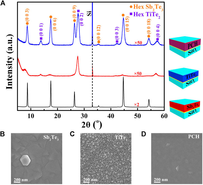
FIGURE 2. (A) XRD curves of ∼100 nm thick Sb2Te3, TiTe2, and PCH films sandwiched between SiO2 layers (see corresponding sketch). All the films were deposited at 300°C on the pregrown seed layer (yellow thin layer in each sketch), exhibiting hexagonal (Hex) lattice configuration with strong c-axis (0 0 l) orientation. For the sake of better observing the weak diffraction peaks, the diffraction intensity is multiplied by 2 for the Sb2Te3 curve and 50 for the TiTe2 and PCH curves. (B–D) SEM images of the in situ heating deposited Sb2Te3, TiTe2, and PCH films, respectively.
Reliable Two-Dimensional Phase Transitions
In the well-textured Sb2Te3/TiTe2 PCH, the TiTe2 blocks with high chemical and thermal stabilities are capable of being the robust confinement layers to restrict the phase transitions of the Sb2Te3 blocks on 2D scale, as demonstrated by the DFMD simulations (Figure 3A). The initial PCH model was heated up to 1,000 K and maintained for 30 ps, where both Sb2Te3 and TiTe2 blocks can still keep crystalline form. As the temperature further increases to 1,300 K, and after 30 ps, the Sb2Te3 block is fully melted, while the TiTe2 block remains to be ordered.
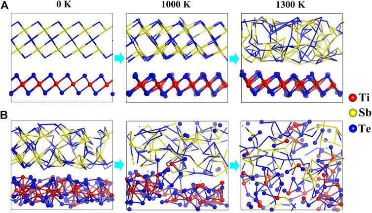
FIGURE 3. (A) DFMD simulations of the melting process of the PCH model. The PCH model is firstly heated up to 1,000 K rapidly within 30 ps. The Sb2Te3 and TiTe2 sublayers are ordered. The Sb2Te3 sublayer is fully melted at 1,300 K after 30 ps, while the TiTe2 sublayer remains in the stable crystalline form. (B) DFMD simulations of the melting process of the SLL model. The SLL model contains partially ordered Sb2Te3 and TiTe2 sublayers. After heating up to 1,000 K for 30 ps, the Sb2Te3 sublayer becomes fully disordered and mixes with the TiTe2 sublayer. As the model is further heated at 1,300 K for 30 ps, the whole model becomes a fully disordered liquid phase.
Regarding the as-deposited and postannealed SLL films of poor crystallinity, there are most likely no clean and nonatomic (van der Waals-like) gaps between their sublayers; therefore the interlayer force cannot be weak enough. The closely bound sublayers may be merged into a compound (bulky) phase upon aggressive RESET operation or extensive programming, making the 3D switching dominate eventually. Our DFMD simulations also qualitatively illustrated such a phenomenon (Figure 3B), where initially the Sb2Te3 and TiTe2 sublayers are chosen to be partially crystallized (or quite disordered) as according to the crystallographic results shown in Figure 1 and Supplementary Figure S2. The SLL model experienced exactly the same heating process as the PCH model. The sublayers in the SLL model are totally disordered after heating at 1,000 K for 30 ps, and the subsequent heating at 1,300 K for another 30 ps finally melts them down into a mixed liquid.
Extended Cycling Endurance and Suppressed Programming Noise
We fabricated the mushroom-type SLL- and PCH-based PCRAM devices with the same geometry (see Materials and Methods section) to draw comparison of their electrical performances. The PCH-based device has lower SET and RESET voltages as compared to those of the SLL-based device (Supplementary Figures S3, S4), correlating to the reduced programming energy. As for the unconstrained 3D phase transitions, PCMs are subjected to nonisothermal and nonequilibrium shocks, giving rise to composition variation upon extensive programming caused by long-range element diffusions along the electrical current direction (Padilla et al., 2010; Xie et al., 2018). Eventually, the device fails due to severe phase segregation and big void formation near the bottom electrode. The SLL-based device underwent repeated 3D phase transitions up to ∼107 cycles until SET sticking failure took place (Figure 4A). We note similar SLL-based device also presented an approximate endurance (Shen et al., 2019), but showing considerably larger resistance fluctuations in both RESET and SET states than those of the SLL-based device studied in this work. The relative standard deviations (RSDs) of RESET and SET states of the SLL-based device are 6.3% (Figure 4C) and 2.2% (Figure 4D), respectively.
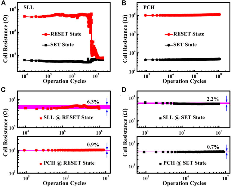
FIGURE 4. (A) Approximately ∼107 cycling endurance of the SLL-based PCRAM device that finally failed due to SET stuck: SET (under 2.1 V) and RESET (under 3.2 V) with 20 ns width voltage pulses. (B) Approximately ∼108 cycles of the PCH device without failure under 10 ns width SET (1.6 V) and RESET (2.4 V) operations voltage pulses. (C) Comparison of the RESET resistance fluctuations between the SLL- and PCH-based device, with the RSD being 6.3 and 0.9%, respectively. (D) Comparison of the SET resistance fluctuations between the SLL- and PCH-based device, with the RSD being 2.2 and 0.7%, respectively.
The reliable 2D phase transitions of the PCH architecture inhibit the large-scale atomic diffusion along the electrical pulse direction, which effectively prolongs the endurance of the PCH-based device to ∼108 cycles without reaching failure (Figure 4B). Note that the fast speed (∼10 ns) and long-life features of the PCH-based device offer a feasible route to develop DRAM-like phase-change working memory technology. Most importantly, the PCH-based device has pretty low resistance fluctuation in both RESET and SET states, with the RSDs being 0.9% (Figure 4C) and 0.7% (Figure 4D), respectively. The ultralow programming noise of the PCH-based device should also be ascribed to the reliable 2D switching manner of the confined Sb2Te3 sublayers, because the randomness of phase transitions (the stochastic crystallization in particular) (Rao et al., 2017) is markedly reduced, leading to more consistent resistance contrast and hence better-defined logic states.
Conclusion
In summary, we have demonstrated that, through fine-tuning the deposition techniques, the multilayer Sb2Te3/TiTe2 stackings can be made into c-axis oriented heterostructure, which shall exhibit weakly coupled interactions among the Sb2Te3 and TiTe2 building blocks. In contrast to the SLL structure that can only execute 3D phase transitions, the PCH architecture is able to perform reliable 2D switching of the confined Sb2Te3 sublayers. The long-range element migration during 3D phase transitions induces device failure after extensive cycling, which can be greatly inhibited in the 2D switching manner, leading to the remarkably extended cycling endurance of the PCH-based device as compared to the SLL-based one. This shall be conducive to the development of nonvolatile and long-life working memory to better renovate the classic von Neumann computing system. And above all, the PCH-based device presents rather smaller resistance fluctuations upon repeated programming than that of the SLL-based device. This low-noise feature is of necessity for the accomplishments of high-accuracy neuromorphic computing tasks.
Data Availability Statement
The raw data supporting the conclusions of this article will be made available by the authors, without undue reservation.
Author Contributions
TL and KD fabricated the films and performed the XRD and SEM tests. KD and FR prepared the device samples and carried out electrical measurements. KD performed ab initio simulations. FR and KD wrote the paper with contributions from BC. All authors discussed the results and commented on the manuscript. The project was initiated and conceptualized by FR.
Funding
This work was supported by the National Natural Science Foundation of China (52032006, 62004130, 62004131), the Basic and Applied Basic Research Foundation of Guangdong (2020B1515120008), and the Science and Technology Foundation of Shenzhen (JCYJ20180507182248605, JCYJ20190808150605474).
Conflict of Interest
The authors declare that the research was conducted in the absence of any commercial or financial relationships that could be construed as a potential conflict of interest.
Supplementary Material
The Supplementary Material for this article can be found online at: https://www.frontiersin.org/articles/10.3389/fnano.2021.649560/full#supplementary-material.
References
Blöchl, P. E. (1994). Projector augmented-wave method. Phys. Rev. B. 50, 17953–17979. doi:10.1103/PhysRevB.50.17953
Boybat, I., Le Gallo, M., Nandakumar, S. R., Moraitis, T., Parnell, T., Tuma, T., et al. (2018). Neuromorphic computing with multi-memristive synapses. Nat. Commun. 9, 2514. doi:10.1038/s41467-018-04933-y
Burr, G. W., Shelby, R. M., Sebastian, A., Kim, S., Kim, S., Sidler, S., et al. (2017). Neuromorphic computing using non-volatile memory. Adv. Phys.-X 2, 89–124. doi:10.1080/23746149.2016.1259585
Chen, B., Chen, Y. M., Ding, K. Y., Li, K. L., Jiao, F. Y., Wang, L., et al. (2019). Kinetics features conducive to cache-type non-volatile phase-change memory. Chem. Mater. 31, 8794–8800. doi:10.1021/acs.chemmater.9b02598
Chia Tan, C., Shi, L. P., Zhao, R., Guo, Q., Li, Y., Yang, Y., et al. (2013). Compositionally matched nitrogen-doped Ge2Sb2Te5/Ge2Sb2Te5 superlattice-like structures for phase change random access memory. Appl. Phys. Lett. 103, 133507. doi:10.1063/1.4823551
Choe, J. (2017). Intel 3D XPoint memory die removed from Intel OptaneTM PCM (Phase Change Memory). Available at: http://www.techinsights.com/about-techinsights/overview/blog/intel-3D-xpoint-memory-die-removed-from-intel-optane-pcm/ (Accessed May 18, 2017).
Chong, T. C., Shi, L. P., Zhao, R., Tan, P. K., Li, J. M., Lee, H. K., et al. (2006). Phase change random access memory cell with superlattice-like structure. Appl. Phys. Lett. 88, 122114. doi:10.1063/1.2181191
Ding, K. Y., Wang, J. J., Zhou, Y. X., Tian, H., Lu, L., Mazzarello, R., et al. (2019). Phase-change heterostructure enables ultralow noise and drift for memory operation. Science 366, 210–215. doi:10.1126/science.aay0291
Ielmini, D., and Wong, H.-S. P. (2018). In-memory computing with resistive switching devices. Nat. Electron. 1, 333–343. doi:10.1038/s41928-018-0092-2
Kestor, G., Gioiosa, R., Kerbyson, D. J., and Hoisie, A. (2013). “Quantifying the energy cost of data movement in scientific applications,” in IEEE International Symposium on Workload Characterization (IISWC), Portland, OR (Newyork, NY: IEEE), 55–65. doi:10.1109/IISWC.2013.6704670
Kresse, G., and Hafner, J. (1993). Ab initio molecular dynamics for liquid metals. Phys. Rev. B. 47, 558–561. doi:10.1103/PhysRevB.47.558
Kuzum, D., Jeyasingh, R. G. D., Lee, B., and Wong, H.-S. P. (2012). Nanoelectronic programmable synapses based on phase change materials for brain-inspired computing. Nano Lett. 12, 2179–2186. doi:10.1021/nl201040y
Lam, C. H. (2010). “Storage class memory,” in 10th IEEE International Conference Solid-State Integrated Circuit Technology, Shanghai, China, November 1–November 4, 2010 (Newyork, NY: IEEE), 1080–1083. doi:10.1109/ICSICT.2010.5667551
Le Gallo, M., Sebastian, A., Mathis, R., Manica, M., Giefers, H., Tuma, T., et al. (2018). Mixed-precision in-memory computing. Nat. Electron. 1, 246–253. doi:10.1038/s41928-018-0054-8
Li, X.-B., Chen, N.-K., Wang, X.-P., and Sun, H.-B. (2018). Phase-change superlattice materials toward low power consumption and high density data storage: microscopic picture, working principles, and optimization. Adv. Funct. Mater. 28, 1803380. doi:10.1002/adfm.201803380
Lu, Y. G., Song, S. N., Song, Z. T., Ren, W. C., Xiong, Y. L., Rao, F., et al. (2012). Superlattice-like GaSb/Sb2Te3 films for low-power phase change memory. Scripta Mater. 66, 702–705. doi:10.1016/j.scriptamat.2012.01.013
Padilla, A., Burr, G. W., Virwani, K., Debunne, A., Rettner, C. T., Topuria, T., et al. (2010). “Voltage polarity effects in GST-based phase change memory: physical origins and implications,” in IEEE International Electron Devices Meeting (IEDM), San Francisco, CA, December 6–December 8, 2010 (Newyork, NY: IEEE). 656–659. doi:10.1109/IEDM.2010.5703444
Rice, J. P., Burke, K., and Ernzerhof, M. (1996). Generalized gradient approximation made simple. Phys. Rev. Lett. 77, 3865–3868. doi:10.1103/PhysRevLett.77.3865
Rao, F., Song, Z., Cheng, Y., Liu, X., Xia, M., Li, W., et al. (2015). Direct observation of titanium-centered octahedra in titanium–antimony–tellurium phase-change material. Nat. Commun. 6, 10040. doi:10.1038/ncomms10040
Rao, F., Ding, K. Y., Zhou, Y. X., Zheng, Y. H., Xia, M. J., Lv, S. L., et al. (2017). Reducing the stochasticity of crystal nucleation to enable subnanosecond memory writing. Science 358, 1423–1427. doi:10.1126/science.aao3212
Rao, F., Zhang, W., and Ma, E. (2019). Catching structural transitions in liquids. Science 364, 1032–1033. doi:10.1126/science.aax6333
Raoux, S., Wełnic, W., and Ielmini, D. (2010). Phase change materials and their application to nonvolatile memories. Chem. Rev. 110, 240–267. doi:10.1021/cr900040x
Saito, Y., Fons, P., Bolotov, L., Miyata, N., Kolobov, A. V., and Tominaga, J. (2016). A two-step process for growth of highly oriented Sb2Te3 using sputtering. AIP Adv. 6, 045220. doi:10.1063/1.4948536
Sebastian, A., Le Gallo, M., Burr, G. W., Kim, S., BrightSky, M., and Eleftheriou, E. (2018). Tutorial: brain-inspired computing using phase-change memory devices. J. Appl. Phys. 124, 111101. doi:10.1063/1.5042413
Shen, J., Lv, S., Chen, X., Li, T., Zhang, S., Song, Z., et al. (2019). Thermal barrier phase change memory. ACS Appl. Mater. Inter. 11, 5336–5343. doi:10.1021/acsami.8b18473
Simpson, R. E., Fons, P., Kolobov, A. V., Fukaya, T., Krbal, M., Yagi, T., et al. (2011). Interfacial phase-change memory. Nat. Nanotechnol. 6, 501–505. doi:10.1038/nnano.2011.96
Soeya, S., Shintani, T., Odaka, T., Kondou, R., and Tominaga, J. (2013). Ultra-low switching power, crystallographic analysis, and switching mechanism for SnXTe100−X/Sb2Te3 diluted superlattice system. Appl. Phys. Lett. 103, 053103. doi:10.1063/1.4817068
Takaura, N., Ohyanagi, T., Tai, M., Kinoshita, M., Akita, K., Morikawa, T., et al. (2014). “55-μA GexTe1-x/Sb2Te3 superlattice topological-switching random access memory (TRAM) and study of atomic arrangement in Ge-Te and Sb-Te structures,” in IEEE International Electron Devices Meeting (IEDM), San Francisco, CA, December 15–December 17, 2014 (Newyork, NY: IEEE). 685–688. doi:10.1109/IEDM.2014.7047132
Tuma, T., Pantazi, A., Le Gallo, M., Sebastian, A., and Eleftheriou, E. (2016). Stochastic phase-change neurons. Nat. Nanotechnol. 11, 693–699. doi:10.1038/nnano.2016.70
Wong, H.-S. P., and Salahuddin, S. (2015). Memory leads the way to better computing. Nat. Nanotechnol. 10, 191–194. doi:10.1038/nnano.2015.29
Wuttig, M. (2005). Phase-change materials: towards a universal memory? Nat. Mater. 4, 265–266. doi:10.1038/nmat1359
Xie, Y., Kim, W., Kim, Y., Kim, S., Gonsalves, J., BrightSky, M., et al. (2018). Self-healing of a confined phase change memory device with a metallic surfactant layer. Adv. Mater. 30, 1705587. doi:10.1002/adma.201705587
Yu, S., and Chen, P. (2016). Emerging memory technologies: recent trends and prospects. IEEE J. Solid-State Circuits Magazine 8, 43–56. doi:10.1109/MSSC.2016.2546199
Keywords: phase-change random-access memory, two-dimensional phase transitions, programming noise, cycling endurance, heterostructure
Citation: Ding K, Li T, Chen B and Rao F (2021) Reliable 2D Phase Transitions for Low-Noise and Long-Life Memory Programming. Front. Nanotechnol. 3:649560. doi: 10.3389/fnano.2021.649560
Received: 05 January 2021; Accepted: 02 February 2021;
Published: 26 March 2021.
Edited by:
Huanglong Li, Tsinghua University, ChinaReviewed by:
Yuta Saito, National Institute of Advanced Industrial Science and Technology (AIST), JapanXinglong Ji, Tsinghua University, China
Copyright © 2021 Ding, Li, Chen and Rao. This is an open-access article distributed under the terms of the Creative Commons Attribution License (CC BY). The use, distribution or reproduction in other forums is permitted, provided the original author(s) and the copyright owner(s) are credited and that the original publication in this journal is cited, in accordance with accepted academic practice. No use, distribution or reproduction is permitted which does not comply with these terms.
*Correspondence: Feng Rao, ZmVuZ3Jhb0BzenUuZWR1LmNu