 Archit Dhingra1,2*
- 1Department of Physics and Astronomy, University of Nebraska−Lincoln, Jorgensen Hall, Lincoln, NE, United States
- 2Carrer del Catedrátic José Beltrán Martinez, Institut de Ciència dels Materials de la Universitat de València (ICMUV), University of Valencia, Valencia, Spain
Layered GeI2 is a two-dimensional wide-bandgap van der Waals semiconductor, which is theorized to be a promising material for thermoelectric applications. While the value of the experimentally extrapolated indirect optical bandgap of GeI2 is found to be consistent with the existing theoretical calculations, its potential as a thermoelectric material still lacks experimental validation. In this Perspective, recent experimental efforts aimed towards investigating its dynamical properties and tuning its bandgap further, via intercalation, are discussed. A thorough understanding of its dynamical properties elucidates the extent of electron-phonon scattering in this system, knowledge of which is crucial in order to open pathways for future studies aiming to realize GeI2-based thermoelectric devices.
Introduction
Pristine layered germanium (II) iodide (GeI2) is a two-dimensional (2D) van der Waals (vdW) material, which is predicted to be thermally stable at temperatures as high as ∼ 600 K (Liu et al., 2018; Hu et al., 2020). Adding to its versatility, for potential nanodevice applications, are its: (i) low cleavage energy (∼0.16 J/m2) (Liu et al., 2018), which is even lower than that of graphite (Zacharia et al., 2004); (ii) calculated appreciable charge carrier mobilities (Liu et al., 2018); (iii) a wide-bandgap (Liu et al., 2018; Hoat et al., 2019; De Andrade Deus and De Oliveira, 2020; Hu et al., 2020; Naseri et al., 2020; Ran et al., 2020; Opoku et al., 2022), which is now experimentally verified (Dhingra et al., 2022b); and (iv) the fact that it can exist without the undesirable edge disorders (Avilov and Imamov, 1968; Urgiles et al., 1996; Liu et al., 2018) that have plagued some well-researched 2D materials (Wimmer et al., 2008; Banhart et al., 2010; Mucciolo and Lewenkopf, 2010; Wurm et al., 2011; Komsa et al., 2012; Dugaev and Katsnelson, 2013; Lo et al., 2014; Shi et al., 2014; Addou et al., 2015; Dong et al., 2015; Lin et al., 2016; Mlinar, 2017; Rosenberger et al., 2018; Blades et al., 2020; Debbarma et al., 2021). Besides being a great candidate for standalone nanodevice applications, its heterostructures have also shown some promise for applications in development of low-power spintronic devices (Shao et al., 2021) as well as for enhancing photocatalytic hydrogen generation performance (Opoku et al., 2022).
In this Perspective, some recent efforts that were aimed towards experimental investigation of the understudied, but highly promising, pristine 2D layered GeI2 are discussed. The main purpose of this article is to comment on the dynamical stability of the 2D layered GeI2, and the intercalation-induced tuning of its bandgap, in the context of its potential as a wide-bandgap thermoelectric material.
Dynamical behavior of the layered GeI2: What do temperature variations do to GeI2?
A fundamental understanding of the effects of temperature variation on any material is indispensable if that material is to be used for thermoelectric applications. Therefore, in this subsection the dynamical behavior of the pristine 2D layered GeI2 is described and discussed. The deterrent effects of the thermal motion of atoms on the physical and electronic properties of materials are well-known (Körmann et al., 2017; Randle et al., 2018; Dhingra et al., 2020; 2021a; 2021b). One certain way to quantify the extent of electron-phonon scattering (or the effects of thermal motion of atoms) in a material is to ascertain its Debye (or effective Debye) temperature. In this regard, temperature dependent x-ray photoemission spectroscopy (XPS) is routinely exploited to determine a system’s effective Debye temperature (Clarke, 1985; Borca et al., 2000; McHale et al., 2011; Evans et al., 2018; Dhingra et al., 2020; 2021a; 2021b).
Figures 1A, B show the temperature dependent XPS spectra of the Ge 2p3/2 core-level and the I 3d5/2 core-level, respectively. The effective Debye temperatures of the Ge 2p3/2 component closer to the surface (the P1 feature of the Ge 2p3/2 core-level) and the I 3d5/2 core-level, as extracted from the linear fits to the Debye–Waller plots in Figures 1C, D, are found to be 186 ± 18 K and 587 ± 31 K, respectively (Dhingra et al., 2022b). It is worth mentioning that, unlike the observed temperature dependence of the photoemission intensities of the P1 feature of the Ge 2p3/2 core-level and the I 3d5/2 core-level, the XPS intensity of the P2 feature of the Ge 2p3/2 core-level is found to increase with increasing temperature (see inset of Figure 1C). Such a direct relationship between the photoemission intensity of the P2 component of the Ge 2p3/2 core-level and temperature implies segregation of germanium in the subsurface (or selvedge) of GeI2 (Dhingra et al., 2022b).
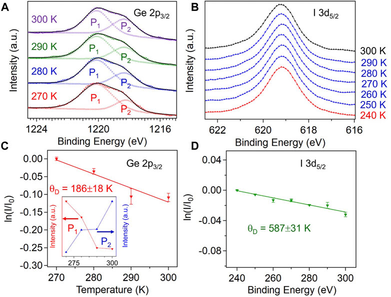
FIGURE 1. (A) Raw XPS of the Ge 2p3/2 core-level (solid markers) collected at temperatures ranging from 270 K to 300 K, along with the total fit (black line). The hollow markers show the P1 and P2 features. (B) XPS spectra of the I 3d5/2 core-level recorded at temperatures ranging from 240 K to 300 K. (C) Debye–Waller factor plot for the P1 feature of the Ge 2p3/2 core-level, as well as the temperature dependence of the XPS intensities of the P1 and P2 components (inset). (D) Debye–Waller plot for the I 3d5/2 core-level (Dhingra et al., 2022b). © IOP Publishing. Reproduced with permission. All rights reserved.
Effects of intercalation: can the bandgap of GeI2 be widened further?
Over the years, intercalation of various 2D materials has resulted in widening of their bandgaps (Eknapakul et al., 2014; Song et al., 2015; Xiong et al., 2015; Wan et al., 2016; Feng et al., 2019). While the pristine GeI2 already has a wide-bandgap, intercalating it with easily synthesizable organic molecules to widen its bandgap further is bound to amplify its utility for low-dimensional high-temperature thermoelectric and optoelectronic applications; and this is exactly what was demonstrated in a recent study (Dhingra et al., 2022a).
Figure 2 shows the Tauc plots through which the direct (Figure 2A) and indirect (Figure 2B) bandgaps of pristine and intercalated GeI2 can be extrapolated (Tauc et al., 1966; Wood and Tauc, 1972). From Figure 2, it is clear that both the direct and indirect optical bandgaps of the pristine GeI2 are in agreement with the ones reported elsewhere (Dhingra et al., 2022b), and the extrapolated direct (indirect) optical bandgaps upon intercalation with the organic molecules, namely: pyridine, aniline, and triethylamine, are found to lie somewhere between 2.9 (2.66)–3.1 (2.92) eV.
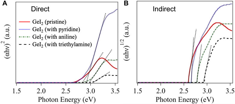
FIGURE 2. Tauc plots for extrapolation of (A) direct and (B) indirect band gaps of the pristine and intercalated GeI2 systems. Reprinted by permission from Springer Nature (Dhingra et al., 2022a), 2022.
Discussion
Theoretically, layered GeI2 is a low-dimensional material that is waiting to get exploited for thermoelectric applications (Hu et al., 2020; Lu and Guan, 2022); nevertheless, there are no experiments to confirm the same. The limited experimentally obtained information that we do have on this exciting nanomaterial suggests that the surface of the layered GeI2 is not stable enough under ambient conditions, and is prone to a large amount of phonon scattering since the effective Debye temperature of the surface is way less than the room temperature (Dhingra et al., 2022b). However, if the complexities encountered at the surface of this material are addressed by depositing a thin layer of a stiff oxide, as has been done for some other quasi-1D materials (Lipatov et al., 2015; Dhingra, 2022), then it may well be possible to realize its potential as a thermoelectric nanomaterial. A stable GeI2 surface with suppressed phonon scattering, when taken together with the ease with which the bandgap of GeI2 can be widened further (Dhingra et al., 2022a), will augment its versatility for high-temperature thermoelectric applications. Finally, it must be noted that as is the case when it comes to forming contacts with most 2D materials (S. Schulman et al., 2018; Ang et al., 2021; Zheng et al., 2021; Dhingra et al., 2020a; Dhingra et al., 2021c; Dhingra et al., 2022c; Dhingra et al., 2022d), forming Ohmic contacts to GeI2 may not be trivial; especially because the germanium rich surface could adversely affect the contact potentials for GeI2-based nanodevices (Dhingra et al., 2022b). This Perspective, thus, acts as a guide for future studies dealing with the GeI2-based thermoelectric nanodevices.
Data availability statement
The original contributions presented in the study are included in the article/supplementary materials, further inquiries can be directed to the corresponding author.
Author contributions
AD wrote the whole manuscript.
Funding
This work was supported by the National Science Foundation through EPSCoR RII Track-1: Emergent Quantum Materials and Technologies (EQUATE), Award No. OIA-2044049; and by the Ministerio de Ciencia e Innovación, which is part of AEI, through the project PID2020-112507GB-I00 (Novel quantum states in heterostructures of 2D materials).
Acknowledgments
The author is grateful to Peter A. Dowben for useful discussions.
Conflict of interest
The authors declare that the research was conducted in the absence of any commercial or financial relationships that could be construed as a potential conflict of interest.
Publisher’s note
All claims expressed in this article are solely those of the authors and do not necessarily represent those of their affiliated organizations, or those of the publisher, the editors and the reviewers. Any product that may be evaluated in this article, or claim that may be made by its manufacturer, is not guaranteed or endorsed by the publisher.
References
Addou, R., Colombo, L., and Wallace, R. M. (2015). Surface defects on natural MoS2. ACS Appl. Mat. Interfaces 7, 11921–11929. doi:10.1021/acsami.5b01778
Ang, Y. S., Cao, L., and Ang, L. K. (2021). Physics of electron emission and injection in two-dimensional materials: Theory and simulation. InfoMat 3, 502–535. doi:10.1002/inf2.12168
Avilov, A. S., and Imamov, R. M. (1968). Electron-diffraction study of germanium diiodide. Kristallografiya 13.
Banhart, F., Kotakoski, J., and Krasheninnikov, A. V. (2010). Structural defects in graphene. ACS Nano 5, 26–41. doi:10.1021/NN102598M
Blades, W. H., Frady, N. J., Litwin, P. M., McDonnell, S. J., and Reinke, P. (2020). Thermally induced defects on WSe2. J. Phys. Chem. C 124, 15337–15346. doi:10.1021/ACS.JPCC.0C04440
Borca, C. N., Komesu, T., Jeong, H.-K., Dowben, P. A., Ristoiu, D., Hordequin, C., et al. (2000). Effective surface Debye temperature for NiMnSb(100) epitaxial films. Appl. Phys. Lett. 77, 88–90. doi:10.1063/1.126886
Clarke, L. J. (1985). Surface crystallography: An introduction to low energy electron diffraction. John Wiley & Sons.
De Andrade Deus, D. P., and De Oliveira, I. S. S. (2020). Tuning the Schottky barrier height in graphene/monolayer-GeI2 van der Waals heterostructure. J. Phys. Condens. Matter 32, 355501. doi:10.1088/1361-648X/ab8bf8
Debbarma, R., Nguyen, N. H. L., and Berry, V. (2021). Defect guided conduction in graphene-derivatives and MoS2: Two-dimensional nanomaterial models. Appl. Mat. Today 23, 101072. doi:10.1016/J.APMT.2021.101072
Dhingra, A., Blair, R. G., and Dowben, P. A. (2022a). Effects of intercalation on bandgap of pristine two-dimensional layered GeI2. MRS Adv. 7, 763–765. doi:10.1557/s43580-022-00302-6
Dhingra, A., Galiy, P. V., Wang, L., Vorobeva, N. S., Lipatov, A., Torres, A., et al. (2020a). Surface termination and Schottky-barrier formation of In4Se3(001). Semicond. Sci. Technol. 35, 065009. doi:10.1088/1361-6641/ab7e45
Dhingra, A., Lipatov, A., Loes, M. J., Sinitskii, A., and Dowben, P. A. (2021a). Nonuniform Debye temperatures in quasi-one-dimensional transition-metal trichalcogenides. ACS Mat. Lett. 3, 414–419. doi:10.1021/acsmaterialslett.1c00094
Dhingra, A., Lipatov, A., Loes, M. J., Abourahma, J., Pink, M., Sinitskii, A., et al. (2022c). Effect of Au/HfS3 interfacial interactions on properties of HfS3-based devices. Phys. Chem. Chem. Phys. 24, 14016–14021. doi:10.1039/D2CP01254E
Dhingra, A., Lipatov, A., Lu, H., Chagoya, K., Dalton, J., Gruverman, A., et al. (2022b). Surface and dynamical properties of GeI2. 2D Mat. 9, 025001. doi:10.1088/2053-1583/ac4715
Dhingra, A., Marzouk, Z. G., Mishra, E., Galiy, P. V., Nenchuk, T. M., and Dowben, P. A. (2020). Indium segregation to the selvedge of In4Se3 (001). Phys. B Condens. Matter 593, 412280. doi:10.1016/j.physb.2020.412280
Dhingra, A., Nikonov, D. E., Lipatov, A., Sinitskii, A., and Dowben, P. A. (2022d). What happens when transition metal trichalcogenides. J. Mater. Res.. doi:10.1557/s43578-022-00744-6
Dhingra, A. (2022). Physical and electronic properties of two-dimensional layered materials: In4Se3, TiS3, ZrS3, HfS3, and GeI2.
Dhingra, A., Sando, D., Lu, P.-S., Marzouk, Z. G., Nagarajan, V., and Dowben, P. A. (2021b). X-ray photoemission studies of BiInO3: Surface termination and effective Debye temperature. J. Appl. Phys. 130, 025304. doi:10.1063/5.0057556
Dhingra, A., Lipatov, A., Sinitskii, A., and Dowben, P. A. (2021c). Complexities at the Au/ZrS3(001) interface probed by x-ray photoemission spectroscopy. J. Phys.: Condens. Matter 33, 434001. doi:10.1088/1361-648X/ac16f8
Dong, L., Wang, J., Namburu, R., O’Regan, T. P., Dubey, M., and Dongare, A. M. (2015). Edge effects on band gap energy in bilayer 2H-MoS2 under uniaxial strain. J. Appl. Phys. 117, 244303. doi:10.1063/1.4922811
Dugaev, V. K., and Katsnelson, M. I. (2013). Edge scattering of electrons in graphene: Boltzmann equation approach to the transport in graphene nanoribbons and nanodisks. Phys. Rev. B 88, 235432. doi:10.1103/PhysRevB.88.235432
Eknapakul, T., King, P. D. C., Asakawa, M., Buaphet, P., He, R.-H., Mo, S.-K., et al. (2014). Electronic structure of a quasi-freestanding MoS2 monolayer. Nano Lett. 14, 1312–1316. doi:10.1021/nl4042824
Evans, P. E., Pink, M., Zhumekenov, A. A., Hao, G., Losovyj, Y., Bakr, O. M., et al. (2018). Rotationally free and rigid sublattices of the single crystal perovskite CH3NH3PbBr3(001): The case of the lattice polar liquid. J. Phys. Chem. C 122, 25506–25514. doi:10.1021/acs.jpcc.8b08994
Feng, N., Meng, R., Zu, L., Feng, Y., Peng, C., Huang, J., et al. (2019). A polymer-direct-intercalation strategy for MoS2/carbon-derived heteroaerogels with ultrahigh pseudocapacitance. Nat. Commun. 10, 1372. doi:10.1038/s41467-019-09384-7
Hoat, D. M., Vu, T. V., Obeid, M. M., and Jappor, H. R. (2019). Tuning the electronic structure of 2D materials by strain and external electric field: Case of GeI2 monolayer. Chem. Phys. 527, 110499. doi:10.1016/j.chemphys.2019.110499
Hu, Y. F., Yang, J., Yuan, Y. Q., and Wang, J. W. (2020). GeI2 monolayer: A model thermoelectric material from 300 to 600 K. Philos. Mag. 100, 782–796. doi:10.1080/14786435.2019.1699670
Komsa, H.-P., Kotakoski, J., Kurasch, S., Lehtinen, O., Kaiser, U., and Krasheninnikov, A. V. (2012). Two-dimensional transition metal dichalcogenides under electron irradiation: Defect production and doping. Phys. Rev. Lett. 109, 035503. doi:10.1103/PhysRevLett.109.035503
Körmann, F., Ikeda, Y., Grabowski, B., and Sluiter, M. H. F. (2017). Phonon broadening in high entropy alloys. npj Comput. Mat. 3, 36. doi:10.1038/s41524-017-0037-8
Lin, Z., Carvalho, B. R., Kahn, E., Lv, R., Rao, R., Terrones, H., et al. (2016). Defect engineering of two-dimensional transition metal dichalcogenides. 2D Mat. 3, 022002. doi:10.1088/2053-1583/3/2/022002
Lipatov, A., Wilson, P. M., Shekhirev, M., Teeter, J. D., Netusil, R., and Sinitskii, A. (2015). Few-layered titanium trisulfide (TiS3) field-effect transistors. Nanoscale 7, 12291–12296. doi:10.1039/c5nr01895a
Liu, C. S., Yang, X., Le, Liu, J., and Ye, X. J. (2018). Exfoliated monolayer GeI2: Theoretical prediction of a wide-band gap semiconductor with tunable half-metallic ferromagnetism. J. Phys. Chem. C 122, 22137–22142. doi:10.1021/acs.jpcc.8b05529
Lo, S.-T., Klochan, O., Liu, C.-H., Wang, W.-H., Hamilton, A. R., and Liang, C.-T. (2014). Transport in disordered monolayer MoS2 nanoflakes—Evidence for inhomogeneous charge transport. Nanotechnology 25, 375201. doi:10.1088/0957-4484/25/37/375201
Lu, N., and Guan, J. (2022). Thermoelectric performance of XI2 (X = Ge, Sn, Pb) bilayers. Chin. Phys. B 31, 047201. doi:10.1088/1674-1056/ac474C
McHale, S. R., McClory, J. W., Petrosky, J. C., Wu, J., Palai, R., Dowben, P. A., et al. (2011). The effective surface Debye temperature of Yb:GaN. Mat. Lett. 65, 1476–1478. doi:10.1016/j.matlet.2011.02.042
Mlinar, V. (2017). Electronic and optical properties of nanostructured MoS2 materials: Influence of reduced spatial dimensions and edge effects. Phys. Chem. Chem. Phys. 19, 15891–15902. doi:10.1039/C7CP03229C
Mucciolo, E. R., and Lewenkopf, C. H. (2010). Disorder and electronic transport in graphene. J. Phys. Condens. Matter 22, 273201. doi:10.1088/0953-8984/22/27/273201
Naseri, M., Hoat, D. M., Salehi, K., and Amirian, S. (2020). Theoretical prediction of 2D XI2 (X=Si, Ge, Sn, Pb) monolayers by density functional theory. J. Mol. Graph. Model. 95, 107501. doi:10.1016/j.jmgm.2019.107501
Opoku, F., Oppong, S. O.-B., Asare-Donkor, N. K., Akoto, O., and Adimado, A. A. (2022). Enhancing the photocatalytic hydrogen generation performance and strain regulation of the vertical GeI2/C2N van der Waals heterostructure: Insights from first-principles study. Energy Adv. 1, 146–158. doi:10.1039/D1YA00047K
Ran, R., Hu, C.-E., Cheng, Y., Chen, X.-R., and Ji, G.-F. (2020). First-principles study of structures, elastic and optical properties of single-layer metal iodides under strain. Z. für Naturforsch. A 75, 877–886. doi:10.1515/zna-2020-0157
Randle, M., Lipatov, A., Kumar, A., Kwan, C.-P., Nathawat, J., Barut, B., et al. (2018). Gate-controlled metal–insulator transition in TiS3 nanowire field-effect transistors. ACS Nano 13, 803–811. doi:10.1021/acsnano.8b08260
Rosenberger, M. R., Chuang, H.-J., McCreary, K. M., Li, C. H., and Jonker, B. T. (2018). Electrical characterization of discrete defects and impact of defect density on photoluminescence in monolayer WS2. ACS Nano 12, 1793–1800. doi:10.1021/ACSNANO.7B08566
Schulman, S., Arnold, D., J., and Das, S. (2018). Contact engineering for 2D materials and devices. Chem. Soc. Rev. 47, 3037–3058. doi:10.1039/C7CS00828G
Shao, D.-F., Ding, J., Gurung, G., Zhang, S.-H., and Tsymbal, E. Y. (2021). Interfacial crystal Hall effect reversible by ferroelectric polarization. Phys. Rev. Appl. 10, 024057. doi:10.1103/PhysRevApplied.15.024057
Shi, Y.-J., Lan, J., Ye, E.-J., Sui, W.-Q., and Zhao, X. (2014). Four-terminal impedance of a graphene nanoribbon based structure. Eur. Phys. J. B 87, 251. doi:10.1140/epjb/e2014-50321-0
Song, S. H., Kim, B. H., Choe, D.-H., Kim, J., Kim, D. C., Lee, D. J., et al. (2015). Bandgap widening of phase quilted, 2D MoS2 by oxidative intercalation. Adv. Mat. 27, 3152–3158. doi:10.1002/adma.201500649
Tauc, J., Grigorovici, R., and Vancu, A. (1966). Optical properties and electronic structure of amorphous germanium. Phys. Stat. Sol. 15, 627–637. doi:10.1002/pssb.19660150224
Urgiles, E., Melo, P., and Coleman, C. C. (1996). Vapor reaction growth of single crystal GeI2. J. Cryst. Growth 165, 245–249. doi:10.1016/0022-0248(96)00193-5
Wan, J., Lacey, S. D., Dai, J., Bao, W., Fuhrer, M. S., and Hu, L. (2016). Tuning two-dimensional nanomaterials by intercalation: Materials, properties and applications. Chem. Soc. Rev. 45, 6742–6765. doi:10.1039/C5CS00758E
Wimmer, M., Adagideli, İ., Berber, S., Tománek, D., and Richter, K. (2008). Spin currents in rough graphene nanoribbons: Universal fluctuations and spin injection. Phys. Rev. Lett. 100, 177207. doi:10.1103/PhysRevLett.100.177207
Wood, D. L., and Tauc, J. (1972). Weak absorption tails in amorphous semiconductors. Phys. Rev. B 5, 3144–3151. doi:10.1103/PhysRevB.5.3144
Wurm, J., Richter, K., and Adagideli, İ. (2011). Edge effects in graphene nanostructures: From multiple reflection expansion to density of states. Phys. Rev. B 84, 075468. doi:10.1103/PhysRevB.84.075468
Xiong, F., Wang, H., Liu, X., Sun, J., Brongersma, M., Pop, E., et al. (2015). Li intercalation in MoS2: In situ observation of its dynamics and tuning optical and electrical properties. Nano Lett. 15, 6777–6784. doi:10.1021/acs.nanolett.5b02619
Zacharia, R., Ulbricht, H., and Hertel, T. (2004). Interlayer cohesive energy of graphite from thermal desorption of polyaromatic hydrocarbons. Phys. Rev. B 69, 155406. doi:10.1103/PhysRevB.69.155406
Keywords: 2D materials, wide-bandgap, van der waals materials, thermoelectric, intercalation, x-ray photoemission spectroscopy, debye temperature
Citation: Dhingra A (2022) Layered GeI2: A wide-bandgap semiconductor for thermoelectric applications–A perspective. Front. Nanotechnol. 4:1095291. doi: 10.3389/fnano.2022.1095291
Received: 11 November 2022; Accepted: 01 December 2022;
Published: 12 December 2022.
Edited by:
Muhammad Sohail Bashir, University of Jinan, ChinaReviewed by:
Yee Sin Ang, Singapore University of Technology and Design, SingaporeCopyright © 2022 Dhingra. This is an open-access article distributed under the terms of the Creative Commons Attribution License (CC BY). The use, distribution or reproduction in other forums is permitted, provided the original author(s) and the copyright owner(s) are credited and that the original publication in this journal is cited, in accordance with accepted academic practice. No use, distribution or reproduction is permitted which does not comply with these terms.
*Correspondence: Archit Dhingra, YXJjaGl0LmRoaW5ncmFAdXYuZXM=