 Niharika Thakuria
 Reena Elangovan
 Sandeep K. Thirumala
 Sumeet K. Gupta
- School of Electrical and Computer Engineering, Purdue University, West Lafayette, IN, United States
We proposed 2D piezoelectric FET (PeFET)–based compute-enabled non-volatile memory for ternary deep neural networks (DNNs). PeFETs hinge on ferroelectricity for bit storage and piezoelectricity for bit sensing, exhibiting inherently amenable features for computation-in-memory of dot products of weights and inputs in the signed ternary regime. PeFETs consist of a material with ferroelectric and piezoelectric properties coupled with a transition metal dichalcogenide channel. We utilized (a) ferroelectricity to store binary bits (0/1) in the form of polarization (−P/+P) and (b) polarization-dependent piezoelectricity to read the stored state by means of strain-induced bandgap change in the transition metal dichalcogenide channel. The unique read mechanism of PeFETs enables us to expand the traditional association of +P (−P) with low (high) resistance states to their dual high (low) resistance depending on read voltage. Specifically, we demonstrated that +P (−P) stored in PeFETs can be dynamically configured in (a) a low (high) resistance state for positive read voltages and (b) their dual high (low) resistance states for negative read voltages, without afflicting a read disturb. Such a feature, which we named as polarization-preserved piezoelectric effect reversal with dual voltage polarity (PiER), is unique to PeFETs and has not been shown in hitherto explored memories. We leveraged PiER to propose a Strain-enabled Ternary Precision Computation-in-Memory (STeP-CiM) cell with capabilities of computing the scalar product of the stored weight and input, both of which are represented with signed ternary precision. Furthermore, using multi-word line assertion of STeP-CiM cells, we achieved massively parallel computation of dot products of signed ternary inputs and weights. Our array-level analysis showed 91% lower delay and improvements of 15% and 91% in energy for in-memory multiply-and-accumulate operations compared to near-memory design approaches based on 2D FET–based SRAM and PeFET, respectively. We also analyzed the system-level implications of STeP-CiM by deploying it in a ternary DNN accelerator. STeP-CiM exhibits 6.11× to 8.91× average improvement in performance and 3.2
1 Introduction
Deep neural networks (DNNs) have transformed the field of machine learning and are deployed in many real-world products and services (Lecun et al., 2015). However, enormous storage and computational demands limit their application in energy-constrained edge devices (Venkataramani et al., 2016). Precision reduction in DNNs has emerged as a popular approach for energy-efficient realization of hardware accelerators for these applications (Courbariauxécole and Bengio, 2015; Mishra et al., 2017; Choi et al., 2018; Colangelo et al., 2018; Wang et al., 2018). State-of-the-art DNN hardware for inference employs 8-bit precision, and recent algorithmic efforts have shown the pathway for aggressive scaling up to binary precision (Choi et al., 2018; Colangelo et al., 2018). However, accuracy suffers significantly at binary precision. Interestingly, ternary precision networks offer a near-optimal design point in the low precision regime with significant accuracy boost compared to binary DNNs (Li et al., 2016; Zhu et al., 2016) and large energy savings with mild accuracy loss compared to higher precision DNNs (Mishra et al., 2017; Wang et al., 2018). Due to these features, ternary precision networks have garnered interest for their hardware realizations (Jain et al., 2020; Thirumala et al., 2020). Ternary DNNs can be implemented using classical accelerator architectures (e.g., tensor processing unit and graphical processing unit) by employing specialized processing elements and on-chip scratchpads to improve energy efficiency, but they are nevertheless limited by memory bottleneck. In this regard, computing-in-memory (CiM) brings a new opportunity that can greatly enhance efficiency of DNN accelerators by reducing power-hungry data transfer between memory and processors.
1.1 Related Works on Low Precision Computing-In-Memory for DNNs
Several previous works have explored hardware realization of low-precision CiM for DNN workloads. For example, binary networks such as XNOR-RRAM (Sun et al., 2018) and XNOR-SRAM (Yin et al., 2020) feature large parallel vector-matrix multiplication capability, but they suffer from low accuracies due to aggressive quantization of weights and inputs to binary values. At the other end of the spectrum, DNNs with 4–8 bits have attained high accuracies, albeit at the cost of considerably increased energy consumption and reduction in throughput (Liu et al., 2015; Chi et al., 2016). In this regard, ternary DNNs are attractive as they achieve a remarkably large upswing in accuracy compared to the binary networks while significantly reducing the energy consumption compared to higher precision networks (Mishra et al., 2017; Wang et al., 2018). In other words, ternary DNNs yield a near-optimal design point in the context of energy–accuracy trade-offs for energy-constrained applications, which has motivated several ternary CiM designs. Yoo et al. (2019) proposed eDRAM-based ternary CiM. However, the repetitive refresh operations add burden to the energy-constrained edge devices. Emerging technologies such as resistive RAM (RRAM) (Chen et al., 2018; Liu et al., 2020; Doevenspeck et al., 2021) and spin transfer/orbit torque magnetic RAM (STT/SOT-MRAM) (Doevenspeck et al., 2020; Bian et al., 2021) are also being actively explored for ternary precision networks due to their high density and low leakage power. However, their power-hungry current driven write (Si et al., 2021) lowers their favorability as a candidate for ternary CiM hardware targeted for energy-constrained environments. The common aspect in all the aforementioned works is that they used signed ternary weights with binary inputs and do not attempt to exploit the accuracy benefits of pure signed ternary networks, that is, with weights = {−1, 0, 1} and inputs = {−1, 0, 1}. Recent works have brought attention to hardware accelerator designs for pure signed ternary regime with static random access memory (SRAM) and non-volatile ferroelectric transistor–based DNN architectures (Jain et al., 2020; Thirumala et al., 2020). These works report high parallelism, low energy, and small accuracy loss, making a case for hardware architectures for signed ternary CiM. However, a downside of both designs is the requirement of hardware additions for achieving ternary CiM functionality. SRAM-based ternary CiM implementations, such as those by Jain et al. (2020), raise concerns for area efficiency and leakage energy. The use of non-volatile ferroelectric transistors in the ternary CiM design (Thirumala et al., 2020) remits area cost and leakage energy. However, existing ferroelectric-based non-volatile memories suffer from other disadvantages that are discussed subsequently.
1.2 Background of Ferroelectric-Based Memories
Ferroelectric RAM or FERAM (Kim et al., 2007) is one of the earliest memories based on ferroelectric materials. It utilizes a ferroelectric capacitor along with an access transistor in a 1T-1C configuration. FERAMs feature high density, large endurance, high retention, and electric field–driven write, which is more energy efficient compared to current-based write in other non-volatile memories (Si et al., 2021). However, it suffers from issues such as destructive read and low distinguishability between the memory states. Ferroelectric FETs (FEFETs), in which the ferroelectric material is integrated within the gate stack of a transistor (Yu et al., 2021), offer appealing attributes that mitigate the concerns of FERAMs. For instance, FEFETs feature separation of read-write paths, non-destructive read, and high distinguishability while retaining the benefits of electric field–driven write (Yu et al., 2021) and offering other advantages such as multilevel storage (Ni et al., 2018; Dutta et al., 2020; Kazemi et al., 2020; Liao et al., 2021). However, they are known to suffer from variability, endurance, and retention concerns due to traps at the ferroelectric–dielectric interface and depolarization fields in the ferroelectric. Moreover, it is challenging to scale their write voltage. In order to achieve write voltage reduction, ferroelectric-metal-FETs (FEMFETs) were proposed by Ni et al. (2018) and Kazemi et al. (2020) which connect a ferroelectric capacitor with the gate of a transistor, allowing independent optimization of the cross-sectional area of two components. This is helpful in scaling the write voltage to logic-compatible levels. The ferroelectric capacitor can be formed directly on the gate stack or at the back-end of the line. In addition to write-voltage reduction, FEMFETs mitigate the variability concerns of FEFETs due to the presence of metal between the ferroelectric and the dielectric of the transistor, which addresses the trap-related issues (Ni et al., 2018; Kazemi et al., 2020). However, this inter-layer metal (ILM) is floating and therefore is susceptible to potential changes due to gate leakage, which leads to bit-sensing challenges (Thirumala and Gupta, 2018).
To address the issues of FERAM, FEFETs, and FEMFETs, while still retaining the advantages of electric field–driven write, we (Thakuria et al., 2020) had explored another flavor of a ferroelectric material–based memory called piezoelectric FET (PeFET). PeFET utilizes both ferroelectric and piezoelectric properties of the ferroelectric material. PeFET consists of a ferroelectric capacitor coupled with a 2D transition metal dichalcogenide (TMD) FET in a four-terminal structure with gate, drain, source, and back contacts. The capacitor is designed with a material exhibiting strong ferroelectric and piezoelectric properties. PeFET utilizes polarization retention of the ferroelectric capacitor for bit storage. Its write operation involves applying suitable voltage across the ferroelectric capacitor to switch the polarization, similar to that of an FERAM. Therefore, PeFETs inherit the advantages of low power electric field–driven switching, large endurance, and high retention. Also, since the ferroelectric layer is controlled by metal layers on both ends, it does not suffer from severe trap-related issues observed in FEFETs. For read, PeFETs employ a unique mechanism based on dynamic bandgap change in the TMD FET induced by voltage-dependent strain of the ferroelectric/piezoelectric capacitor. This leads non-destructive read and separation of read-write paths (discussed later). Furthermore, there is no floating metal in PeFETs (unlike FEMFETs). This prevents issues related to gate leakage. One design challenge in PeFETs is limited distinguishability, which can be improved by choosing ferroelectric material exhibiting high piezoelectricity, for example, PZT-5H (Malakooti and Sodano, 2013) and TMD material with high sensitivity of bandgap change to pressure, for example, MoS2 (Peña-Álvarez et al., 2015) and geometry optimization such as hammer and nail effect (Newns et al., 2012) to focus the strain on the TMD channel. These aspects are discussed in detail later. In summary, PeFETs address several important challenges observed in existing ferroelectric-based memories while retaining the key advantage of electric field–driven write. In addition, as proposed in this work, they exhibit unique properties associated with polarization-induced strain that make them amenable for designing compute-enabled memories in the pure signed ternary regime.
1.3 Previous Works on Piezoelectric-Based FETs
Initial proposals of piezoelectric-based FETs were made in the context of steep-switching devices (Newns et al., 2012; Hueting et al., 2015; Das, 2016; Wang et al., 2018; Alidoosty-Shahraki et al., 2019). A material with high piezoelectric coefficient, such as lead magnesium niobate–lead titanate (commonly known as PMN-PT) is utilized in such devices to modulate the resistance of a piezoresistive material (Newns et al., 2012) or bandgap of the Si/TMD channel (Hueting et al., 2015; Das, 2016; Alidoosty-Shahraki et al., 2019). Our proposal of PeFET (Thakuria et al., 2020) extends the idea of piezoelectricity-driven bandgap modulation of TMD beyond steep-switching devices to non-volatile memory (NVM) design. As already introduced, it stores bit information in a piezoelectric/ferroelectric material and leverages polarization-dependent piezoelectric response to modulate the bandgap of the TMD channel for sensing. As shown by Thakuria et al. (2020) and discussed later, positive ferroelectric polarization (+P) leads to bandgap reduction in TMD and thus low resistance state (LRS). On the other hand, negative polarization (−P) yields bandgap increase and high resistance state (HRS). The drain current of PeFET can be used to sense the memory. Contrary to previous proposals of piezoelectric-based FETs, PeFET NVM uses lead zirconate titanate (PZT-5H) as piezoelectric (PE) to satisfy the following requirements: (i) sufficiently wide hysteresis of polarization–voltage response for non-volatile memory functionality (ferroelectric property) and (ii) large strain–voltage characteristics (piezoelectric property) for achieving effective bandgap modulation in TMD NVM. Various experiments have demonstrated monotonic bandgap reduction in TMD on the application of out-of-plane pressure (Nayak et al., 2014; Peña-Álvarez et al., 2015). For example, multilayer molybdenum disulfide (MoS2) subjected to out-of-plane uniaxial stress has experimentally shown a bandgap reduction of ∼80 meV/GPa and achieves semiconductor-to-metal transistor at ∼20 GPa (Nayak et al., 2014). Monolayer MoS2 achieves bandgap reduction of up to ∼800 meV/GPa (Peña-Álvarez et al., 2015). We use monolayer MoS2 in this work due to its high bandgap coefficient.
1.4 Contributions in This Work
In this study, we identified that the unique read mechanism of PeFET can be extended beyond standard memory implementation proposed in Thakuria et al. (2020). We build on this understanding to present PeFET-enabled signed ternary CiM design. The key contributions of this study are as follows:
1. We established through simulations that LRS of +P can be swapped to HRS while HRS of −P to LRS by reversing the polarity of applied voltage across the piezoelectric during sensing. We named this feature as polarization preserved piezoelectric effect reversal with dual voltage polarity (PiER).
2. We explored PiER for ternary input encoding. We show that PiER motivates exploration of PeFET-based non-volatile memory that naturally supports signed ternary CiM.
3. We proposed a ternary compute-enabled non-volatile memory (STeP-CiM) using PeFET and PiER functionality that performs scalar multiplication of signed inputs and weights without extra transistors.
4. We showed parallel in-memory dot product computation with STeP-CiM based on current sensing, as opposed to voltage sensing in the previous ternary designs by Jain et al. (2020) and Thirumala et al. (2020). We discussed the implications of current sensing for signed ternary CiM and evaluated the energy and delay of STeP-CiM in comparison to near-memory (NM) baselines based on PeFET (PeFET-NM) and SRAM (SRAM-NM).
5. We evaluated the system-level implications of STeP-CiM by implementing it in a DNN accelerator and quantify its energy, performance benefits and tradeoffs over PeFET-NM and SRAM-NM baseline designs.
2 Device Structure, Materials, and Methods of Modeling and Simulation
2.1 Device Structure and Operation of PeFET
PeFET is a four-terminal non-volatile device consisting of drain (D), gate (G), source (S), and back (B) contacts. We present the structure and schematic of a PeFET device in Figures 1A,B. Its non-volatility is enabled by a ferroelectric material (PE) positioned between G and B, which also functions as the write port of the device, as illustrated in Figure 1A. In addition to ferroelectricity, PE, which is PZT-5H in this work, exhibits good piezoelectric response (high piezoelectric coefficient value, d33 = 650 p.m./V (Malakooti and Sodano, 2013) for successful sensing. On the other side of G, an oxide layer of Al2O3 is deposited and a 2D-TMD channel of monolayer MoS2 is grown over it. The monolayer MoS2 undergoes bandgap change caused by the transfer of polarization-induced strain from PE to TMD. We select MoS2 due to its high coefficient of bandgap change for applied pressure,
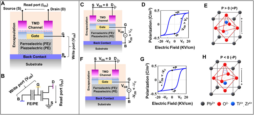
FIGURE 1. (A) Device structure of PeFET showing its four terminals, namely, back (B), drain (D), gate (G), and source (S). Ferroelectric or piezoelectric (FE/PE) material that extends non-volatile feature to PeFET is placed between G and B terminals. (B) Schematic representation of PeFET. Ferroelectric-based storage in PeFET. (C) Bias conditions of PeFET for +P polarization switching. (D) Polarization vs. electric field response showing +P switching behavior for VGB > VC in PZT-5H, extracted from the experimental result by Malakooti and Sodano (2013). (E) Structure of PZT in the +P stable state. (F) Bias conditions of PeFET for −P polarization switching. (G) Polarization vs. electric field response showing −P switching behavior for VGB < −VC in PZT-5H, extracted from the experimental result by Malakooti and Sodano (2013). (H) Structure of PZT in the −P stable state.
PE stores binary bit information (1 or 0) in the form of stable polarization states (+P or −P). The polarization state is controlled by voltage at the write port or gate to back voltage (VGB) as illustrated by Figures 1C–H. To write +P (logic 1), we apply VGB = VDD > VC, where VC is the coercive voltage of PZT-5H (Figure 1C). VGB > VC induced +P switching is shown by the polarization–electric field (P-E) response in Figure 1D. On the contrary, application of VGB < −VC causes polarization to switch to −P state (or logic 0), as signified in Figures 1F,G. At a structural level, a perovskite material such as PZT-5H exist in +P (or −P) polarized state due to upward (or downward) displacement of Ti4+/Zr4+ from their centrosymmetric position, as depicted in Figures 1E,H.
To read the stored polarization in FE, we apply a positive voltage (VR) across G and B. We present a description of the read mechanism in PeFET through Figure 2. First, VR < |VC| is applied to ensure that current state of polarization in PE is not disturbed. VR has the following role: (i) it actuates strain (piezoelectric effect) in the PE, which is in turn transduced to the TMD channel and (ii) simultaneously turns on the TMD channel. If +P had been stored in the PE, VR enhances charge separation along the direction of polarized charge, as shown in Figure 2A. This causes an increase in PE thickness (
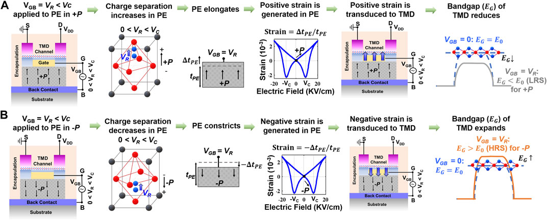
FIGURE 2. Mechanism of polarization-dependent strain transduction in PE that enables read operation in PeFET. (A) PeFET with +P showing bandgap reduction and (B) PeFET with −P showing bandgap expansion from intrinsic position on application of read voltage that is 0 < VR < VC. The baseline for bandgap comparison is PeFET with VGB = 0.
2.2 Modeling and Simulation
To perform circuit simulations of PeFET, we employ a simulation framework that integrates HSPICE, COMSOL, and Verilog A–based models of various components in PeFETs. A representation of the modeling framework is provided in Figure 3. First, we discuss the HSPICE-based circuit-compatible model, Miller model, used for capturing the ferroelectric behavior of PE. The equivalent circuit of the PE is shown in Figure 3. We utilize Eqs 1, 2 to simulate the polarization–electric field switching behavior of PE. Figure 4A presents calibration of the simulated P-E characteristics with experimental characterization of PZT-5H by Malakooti and Sodano (2013). The hysteresis window of P-E response of PZT-5H is 18 kV/cm with EC = 9 kV/cm (Malakooti and Sodano, 2013). The calibrated values of saturation polarization (PS), remnant polarization (PR), coercive electric field (EC), and dielectric permittivity (
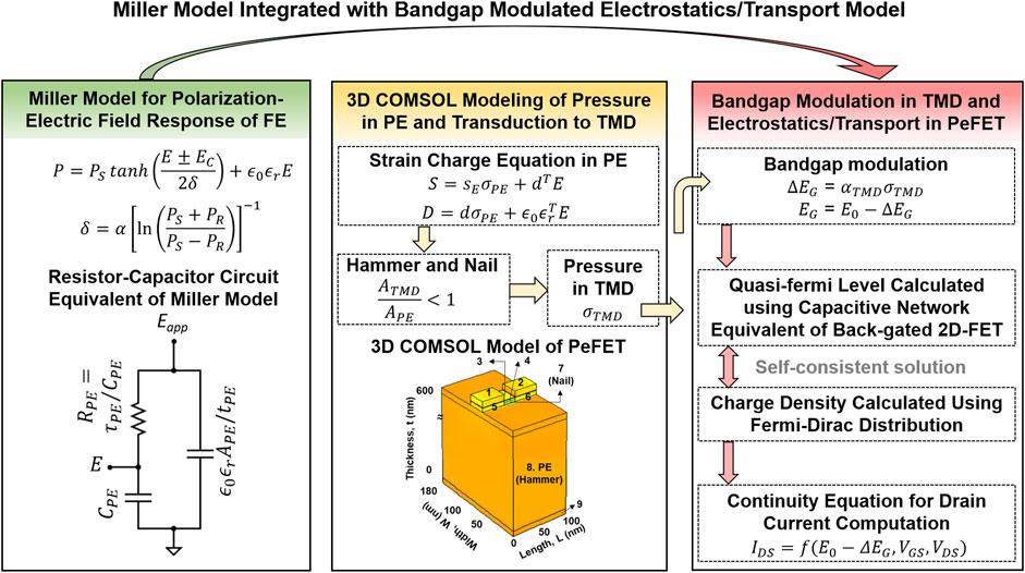
FIGURE 3. HSPICE-compatible model of PeFET formed by integrating (i) Miller model of polarization–electrical field behavior of PE, (ii) 3D COMSOL model of PeFET simulating pressure in PE and its transduction to TMD on application of gate voltage, and (iii) electrostatics and transport model of TMD augmented with bandgap modulation behavior.
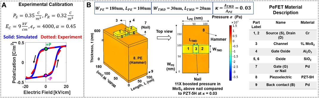
FIGURE 4. (A) Calibration of simulated polarization-electrical response with experiments. (B) 3D COMSOL model of PeFET with components labeled, their material specification, and top view of PeFET signifying hammer which is the top surface area of PE (8) and nail which is the gate below active MoS2 (7). Pressure in MoS2 in the active/nail region is ∼11× higher than PE.
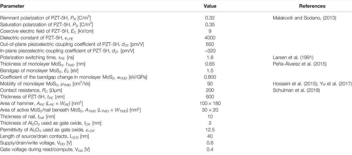
TABLE 1. Parameters used in the PeFET model.
Next, we model a 3D structure of PeFET in COMSOL Multiphysics Suite (Figure 3) that integrates solid mechanics, electrostatics, and their couplings using Eqs 4–7. Using this model, we analyze piezoelectric effect in PE and transduction of stress to 2D-TMD during read. We employ strain–charge Eqs 4, 5 to our 100 nm × 180 nm × 600 nm PE composed of PZT-5H. To obtain strain in PE (SPE), we provide VR = 0.4 V to the gate contact (labeled as 7 in Figure 4B). Therefore, E across PE = VR/tPE = 6.7 kV/cm. E translates to strain by means of piezoelectric coupling coefficients, d. We use parameter values of d (d33 and d31) that are reported in Malakooti and Sodano (2013) based on experimentally characterized strain vs. electric field response of PZT-5H. Stress in PE
Furthermore, to boost efficiency of transduction of stress from PE (σPE) to TMD (σTMD), we incorporate the hammer and nail effect. Hammer and nail is effective when the area of nail/2D-TMD (ATMD) is sufficiently smaller than that of PE (APE), that is, ATMD < APE. Smaller ATMD than APE allows stress from PE (hammer labeled as 8 in Figure 4B) to be better localized to TMD that lies above the nail (label 3, 7 in Figure 4B), thereby facilitating efficient transfer. We define a device parameter
Here,
We use σTMD obtained from the COMSOL model as input to the Verilog A model of 2D-TMD FET. This model first converts σTMD to a bandgap change,
where E0 is the bandgap of TMD at zero gate to back voltage.
Finally, the HSPICE compatible model of PeFET is a combination of Miller equation for PE/FE with the polarization-induced piezoelectric response incorporated 2D-TMD FET model. The parameters used in our simulations are based on prior literature and experiments (Table 1).
3 Characteristics of 2D Piezoelectric FET
3.1 Strain Transfer Through the Hammer-and-Nail Principle
To analyze the hammer and nail principle in our 3D COMSOL model of PeFET (Figure 4B), we use WPE = 180 nm that results in
Tuning of
3.2 Device Characteristics of PeFET
Let us start with a brief discussion on the biases required for
Now, we divulge into the polarization/strain-dependent transfer characteristics (IDS-VGS) of PeFET. To avoid polarization switching while obtaining transfer characteristics, we apply a positive gate voltage VG = VR = 0.4 V (< VC of PZT-5H = 0.54 V at
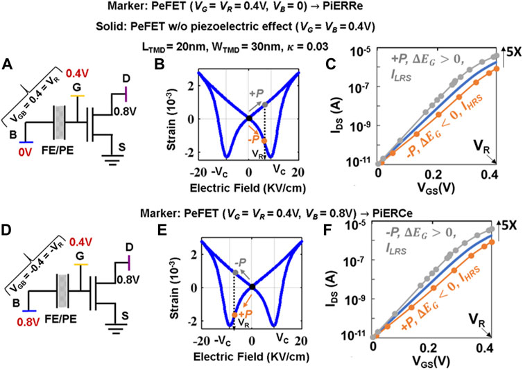
FIGURE 5. (A) Schematic representation of PeFET for VG = 0.4 V, VB = 0 V, VGB = 0.4 V > 0, or PiERRe mode. (B) Strain–electric field response for VGB = VR > 0. (C) Device characteristics for VGB > 0. (D) Schematic representation of PeFET for VG = 0.4 V, VB = 0.8 V, VGB = −0.4 V < 0, or PiERCe mode. (E) Strain–electric field response for VGB = −VR < 0. (F) Device characteristics for VGB < 0.
When VGB = VR = 0.4 V is applied, PeFET with +P undergoes positive strain in PE (follow gray arrow in Figure 5B) that results in bandgap reduction
Let us now present the PiER characteristics of PeFETs, which is associated with the dependence of PeFET characteristics on the polarity of VGB and eventually enables us to design signed ternary CiM.
3.3 Polarization Preserved Piezoelectric Effect Reversal With Dual Voltage Polarity
Until now, our analyses focused on piezoelectric response generated when PE is subjected to VGB = VR > 0. Recall that we maintain VB = 0, while sweeping VG to VR to achieve the same. With this bias, PeFET in +P yields LRS whereas −P leads to HRS (Figure 5C).
Interestingly, the sensed resistance states with
We elucidate the reversal of piezoelectric effect and its impact on the TMD resistance now. Let the stored polarization in PE be −P. When VGB = −VR, charge separation occurs in the same direction as that of initial polarization. This causes

TABLE 2. Summary of bias conditions and the PeFET resistance state with PiERRe and PiERCe modes.
From our analysis of PeFET device characteristics in PiERCe configuration (Figure 5F: VG = 0.4 V, VB = 0.8 V, and VGB = −0.4 V), we observe that PeFET with −P exhibit 2.3× larger drain current (ILRS) whereas that with +P shows 2.2× lower drain current (IHRS) compared to baseline (i.e., PeFET without bandgap modulation: VGB = 0). Overall, distinguishability = ∼5× is achieved, which is similar to that for read described in Section 3.2, but with polarization state mapping to LRS and HRS swapped.
Note that we use strain-independent electron mobility,
4 Ternary Compute–Enabled Memory Based on Pefet
In this section, we propose a PeFET-based non-volatile memory with the capability to perform dot product computations in the signed ternary regime. We refer to the proposed memory as Strain-enabled Ternary Precision Computation-in-Memory (STeP-CiM).
4.1 STeP-CiM Cell
STeP-CiM presented in Figures 6A,B consists of two PeFET-based bit cells (M1 and M2). M1 and M2 store bit information (1/0) in the form of +P/−P polarization. M1 and M2 use 2D TMD FET–based access transistors (AX1, AX2, RAX1, and RAX2) that are switched on/off using word line (WL). Access transistors AX1 and AX2 connect bit lines BL1 and BL2 with the gate terminals (G1 and G2) of the respective PeFETs M1 and M2. Recall that the gate terminal is a common control knob for the channel of the 2D-TMD FET and PE in M1/M2. Hence, BL1 and BL2 can actuate ferroelectric switching for write as well as piezoelectric response in PE for read/compute depending on the voltage they are driven to. The bias conditions of BL1/BL2 and impact on write-read-compute operation are discussed in detail in Section 4.2 and Section 5. Note that RAX1 and RAX2 are read access transistors that connect drains (D1 and D2) of PeFETs in M1 and M2 to read bit lines RBL1 and RBL2, respectively. The back terminals of PeFETs in M1 and M2 are shared and connected to compute word line, CWL. Read and compute are achieved by sensing strain-induced resistance changes in the PeFETs (more in Section 4.2.2 and Section 5) in terms of RBL1 and RBL2 currents. During hold, voltages of BL1, BL2, RBL1, RBL2, CWL, and WL are 0 V.
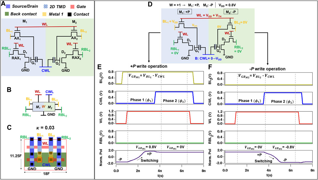
FIGURE 6. Non-volatile memory cell for STeP-CiM showing (A) Schematic illustration, (B) symbol, and (C) layout. (D) Schematic representation of the STeP-CiM cell with an example of biases for write operation (ternary 1). Two-phase write operation depicting in (E) −P
It should be noted that M1/M2 of STeP-CiM cell can be used as standard memory with binary storage. Hence, STeP-CiM cell can be reconfigured to serve as a standard memory (with 2 bit cells) or a compute-enabled memory for ternary precision as per application needs (further discussion on this in Section 6). Using two access transistors (such as AX1 and RAX1 in M1) does not lead to any area penalty in the layout shown in Figure 6C. This is because the layout area is dictated by the PeFET footprint arising from the wide PE requirement for hammer and nail effect. As per our layout analysis, both AX and RAX can be accommodated within the PE layout area.
The access transistors in STeP-CiM cell (AX1, AX2, RAX1, and RAX2) serve two other purposes, in addition to achieving selective access to the cells in a memory array. First, AX1/AX2 of the un-accessed cells disconnect BL1/2 from the respective PE capacitance, which is large due to high dielectric permittivity of PZT-5H,
4.2 Write and Read Operations of STeP-CiM Cell
4.2.1 Write
The encoding for signed ternary weights stored in a STeP-CiM cell is provided in Table 3A. To store ternary “1” in STeP-CiM, +P and −P are written in M1 and M2 as per Table 3A. This operation is depicted by Figures 6D–F. First, BL1 is driven to VDD > VC and BL2 to 0 V. RBL1/2 are kept at 0 V. Next, WL is asserted to VDD + VTH (boosted to compensate for threshold voltage VTH drop in write access transistors). Finally, CWL is supplied with a two-phase signal (
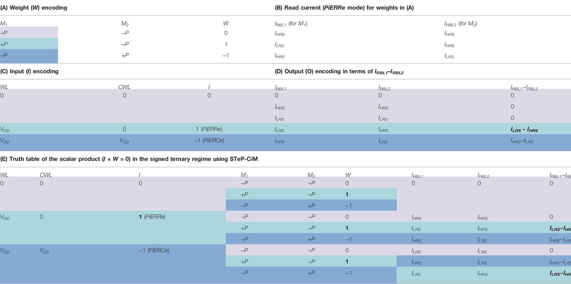
TABLE 3. Signed ternary scheme of {−1, 0, 1} in (A) weights (W) represented in terms of polarization stored in PeFETs M1 and M2. (B) Sensed states of weights. (C) Inputs (I) encoded utilizing biases in word line (WL) and read word line (CWL). It should be noted that the inputs place PeFETs M1 and M2 into different resistance regimes, PiERCe and PiERRe. (D) Outputs (O) used for MAC computation in STeP-CiM. Subtracted currents on read bit lines RBL1 and RBL2 signify ternary outputs. (E) Truth table of the scalar product in the signed ternary regime using STeP-CiM.
4.2.2 Read
In order to sense the stored polarization value in the STeP-CiM cell, a positive VGB (= VR < VC) need to be applied across the PEs of M1 and M2 for them to be in PiERRe condition (refer to Table 2). Moreover, gates G1 and G2 of M1 and M2 should receive VR for PeFETs to conduct. To achieve this, we drive BL1 and BL2 to VR = 0.4 V while CWL is kept at 0 V. In addition, RBL1 and RBL2 are switched to VDD = 0.8 V to facilitate drain to source conduction of PeFETs. The schematic with biases for the read operation and waveform are demonstrated in Figures 7A,B.
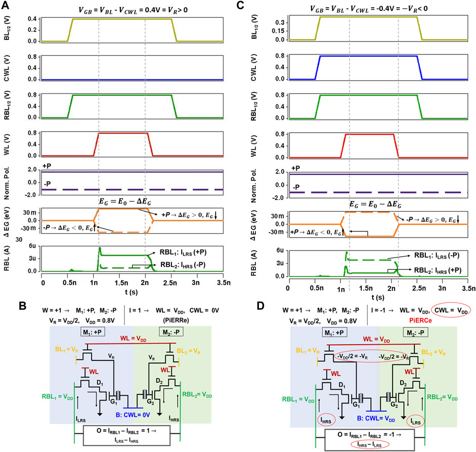
FIGURE 7. Waveform of (A) read operation showing ILRS for +P and IHRS for −P when VGB = VR (PiERRe mode). This waveform and schematic representation in (B) show scalar product with W = 1 (+P in M1 and −P in M2) and I = 1 (corresponding to CWL = 0 V and WL = VDD), resulting in ILRS on RBL1 due to +P in M1 and IHRS on RBL2 due to −P in M2. (C) Waveform and schematic representation in (D) depicting the scalar product with W = 1 (+P in M1 and −P in M2) and I = −1 (in the PiERCe mode corresponding to CWL = VDD and WL = VDD). This results in IHRS on RBL1 due to +P in M1 being sensed as HRS due to I = −1 and ILRS on RBL2 due to −P in M2 being sensed as LRS due to I = −1. For the same weights, currents on RBL1 and RBL2 for I = 1 (waveform A) are swapped for I = −1 (waveform B) due to difference in CWL (highlighted with red circles).
On asserting WL with VDD = 0.8 V, VGB = VBL1/BL2−VCWL = 0.4 V for both M1 and M2. Let us explore the sensing of ternary “1”. In this case, as +P is stored in M1, bandgap reduces (
4.3 Segmented Architecture of STeP-CiM
If standard memory array architecture is followed for STeP-CiM cell wherein CWL runs throughout the row, CPE from all cells in the row add to CWL capacitance. This could lead to large energy overheads (Thakuria and Gupta, 2022), since CPE for PZT-5H is large (as discussed before). To mitigate this, we design an array for STeP-CiM that employs segmentation similar to FERAMs (Rickes et al., 2002). Figure 8 illustrates the segmented array architecture of STeP-CiM-based cells. Segmentation may not be required for CiM in DNNs that utilize high parallelism by computing the dot products for all the columns simultaneously. However, if this proposed array is used as a standard memory (as discussed before), segmentation will be important for high energy efficiency, especially in edge devices. Therefore, we employ the segmented architecture with an objective to support the reconfiguration of the proposed design from a compute-enabled ternary memory for DNNs to a standard memory, as per the application needs.
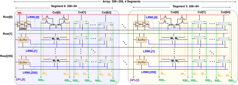
FIGURE 8. Segmented array of STeP-CiM of size 256 × 256, comprising 4 segments, each of size 64 × 256.
A segment in the segmented array (Thakuria and Gupta, 2022) is sized as 64 × 256 (Figure 8). Each segment has an exclusive global plate line (GPL) that runs along the column direction. GPL acts as an input to buffers in each local row of the segment. The output of the buffers is used to drive a local read word line LCWL for each local row comprised of 64 STeP-CiM cells. Notice that, the capacitance on LCWL is from CPE of 64 STeP-CiM cells instead of the entire row, which enhances the energy efficiency. WL provides the supply voltage to the buffers and also activates access transistors of each STeP-CiM in the accessed segment. Bit lines BL1, BL2, RBL1, and RBL2 run along the column. The 64 STeP-CiM cells in a segmented row are accessed simultaneously for read and write.
Appropriate biasing of GPL during write and read operations is important to ensure that LCWL voltage is identical to CWL voltage discussed in Section 4.2. For write, we apply the two phase 0 → VDD signal to GPL, instead of CWL in Section 4.2.1. When WL is asserted with VDD + VTH, LCWL is driven to 0 → VDD + VTH by the active buffers connected to GPL and LCWL. VGB = VDD in
5 In-Memory Ternary Computation Using STeP-CiM
In this section, we explain ternary in-memory scalar multiplication and dot product computation using STeP-CiM. We target signed ternary precision for weights, inputs, and the scalar product having values {−1, 0, 1} (Li et al., 2016). As discussed in Section 4.2.1, combination of polarization states of M1 and M2 in STeP-CiM constitute a ternary weight (Table 3A). The ternary inputs encoded with WL and CWL voltages to utilize the resistance states of both conditions, PiERRe (CWL = 0) and PiERCe (CWL = VDD = 0.8 V), are indicated in Table 3C. More details on this are as follows. BL1 and BL2 are driven to VR = 0.4 V so that VGB < |VC| appears across PE of M1 and M2 (similar to Section 4.2.2). RBL1 and RBL2 are driven to VDD during compute. In accordance with the ternary weights and applied input, different instances of RBL1 and RBL2 currents (IRBL1 and IRBL2) are observed. Finally, the scalar product or output is obtained as O = IRBL1−IRBL2. Notice from Table 3D that O = {−1, 0, 1} is interpreted as {(IHRS–ILRS), 0, (ILRS–IHRS)}, respectively.
5.1 Ternary Scalar Multiplication Using STeP-CiM
Before delving into details of ternary scalar multiplication with STeP-CiM, we elaborate on what the input encoding (I) in Table 3C represents in terms of resistance states. Subsequently, we evaluate examples of ternary scalar multiplication. The truth table for scalar product is available in Table 3E.
5.1.1 Ternary input (I) = +1
I = +1 corresponds to CWL = 0 and WL being asserted with VDD. With BL1 and BL2 being VR during compute (as mentioned before), we have VGB1,2 = VBL1,2−VCWL = VR for I = +1. Note that VGB, being a positive voltage here, puts PeFETs in PiERRe resistance regime (corroborating with Table 2). That is, +P is read as LRS (ILRS) and −P as HRS (IHRS). With this background, we elaborate the scalar products for different weight (W) conditions with I = +1 (for which PeFETs are in PiERRe). Please refer to Table 3E for further clarity on the descriptions of W, I, and corresponding O.
(a) W = +1: According to this weight encoding, M1 and M2 store +P and −P, respectively. Since, PeFETs are in PiERRe because of I = +1, M1 and M2 are in LRS and HRS, respectively. Hence, IRBL1 = ILRS, IRBL2 = IHRS, and O = W×I = ILRS–IHRS. O corresponds to scalar product of +1 in Table 3E. Figures 7A,B shows the waveform for this example.
(b) W = −1: M1 and M2 are written with −P and +P, respectively; hence, they exhibit HRS and LRS for I = 1. Hence, IRBL1 = IHRS, IRBL2 = ILRS, and O = IHRS–ILRS corresponding to scalar product = −1.
(c) W = 0: Both M1 and M2 have −P stored in them and are in HRS for I = 1. Thus, IRBL1 = IHRS, IRBL2 = IHRS, and O = IHRS−IHRS = 0 (corresponding to scalar product of 0).
5.1.2 Ternary input (I) = −1
For I = −1, CWL and WL are both switched to VDD. Since, BL1 and BL2 remain at VR (= VDD/2) during compute, we have VGB1,2 = VBL1,2−VCWL = −VDD/2 = −VR for I = −1. With VGB < 0, now PeFETs M1 or M2 are in PiERCe resistance regime. Hence, +P and −P are sensed as HRS (IHRS) and LRS (ILRS). Note that the sensed states are reversed for the same stored polarization compared to previous example due to PiERCe (refer to Section 3.3 for detailed mechanism). The scalar products with I = −1 for varying weights are evaluated as follows.
(a) W = +1: Although M1 and M2 have +P and −P stored in them [same as in example 5.1(a)], they now exhibit HRS and LRS, respectively, now due to PeFETs being in PiERCe. This is caused by interaction of the stored polarization with negative VGB (refer to Table 2) when I = −1. Ultimately, IRBL1 = IHRS, IRBL2 = ILRS, and O = IHRS–ILRS = −1 (Table 3E). Figures 7C,D represent this example with waveforms, highlighting the differences from I = 1 and W = 1.
(b) W = −1: In this case, polarization in M1 and M2 is −P and +P, respectively. Due to PiERCe, IRBL1 = ILRS, IRBL2 = IHRS, and O = ILRS–IHRS = +1.
(c) W = 0: With M1 and M2 both storing −P and −P. Hence, O = ILRS−ILRS = 0.
5.1.3 Ternary Input (I) = 0
In this case, CWL and WL are de-asserted with 0 V. PeFETs are non-conducting. IRBL1 and IRBL2 are 0V, hence O = 0, irrespective of the weights.
5.2 Ternary Multiply-and-Accumulate With STeP-CiM
In this section, we elaborate on the design details of a STeP-CiM array for achieving ternary MAC, with reference to the schematic in Figure 9A. Prior to the operation, weight vector with Wis is mapped and programmed to M1i and M2i of each row of STeP-CiM, following the procedure discussed in Section 4.2.1. The input vector (Ii) encoded as WL and CWL voltages is applied to the rows accessed for MAC. Currents flowing through RBL1 and RBL2 due to scalar product of Ii and Wi add up on the respective lines. These currents are used to evaluate the dot product. Our method for current-based sensing is as follows: first, we compare IRBL1 and IRBL2 to determine which branch has higher current. The output of the comparator in Figure 9B determines the sign (Sn) of the final MAC output. If IRBL1 > IRBL2, Sn = 1, whereas for IRBL1 < IRBL2, Sn = −1. Next, the comparator output is fed to a current subtractor circuit (Figure 9C), which determines the magnitude of the difference of bit currents, IRBL1−IRBL2. The output of the subtractor is actually an integer multiple of ILRS–IHRS, that is, IRBL1−IRBL2 = a (ILRS–IHRS), where “a” is the integer multiple. To determine the value of “a”, we employ a flash analog to digital converter (ADC), as in Figure 9D. Finally, the dot product is computed as O = Sn
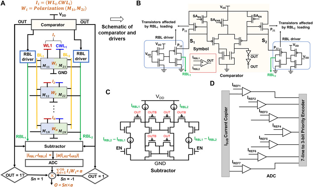
FIGURE 9. (A) Column of the STeP-CiM cell for MAC operation. In the schematic representation, we labeled weights (W) as combination of polarization in M1i and M2i conforming to encoding in Table 3A, while inputs of a cell are encoded utilizing WL and CWL, according to Table 3C. Peripherals used in the simulation of a MAC operation such as comparators, read drivers, subtractors, and ADC are shown. Schematic representation of (B) read drivers interacting with RBL and comparator. (C) Subtractor and (D) 3-bit ADC represented using symbol in inset of (B).
Next, we throw light on the design of our peripherals and the non-idealities caused by their interaction with current-based sensing scheme for MAC. The read bit line drivers in Figures 9A,B used for biasing RBL1 and RBL2 to VDD during MAC operation (as per the biasing scheme discussed in Section 5) are the primary source of non-idealities. Note in Figure 9B that the transistor P11 (P21) of the comparator is connected in series to transistor P12 (P22) of read bit line driver, with drain of P12 (P22) connected to RBL1 (RBL2). Although this configuration is necessary for mirroring RBL1 and RBL2 current to the comparator required for MAC (whose functionality we have discussed previously), rising current on RBL1 (RBL2) with multiple row access causes voltage on the source node S1 (or S2) of P12 (P22) to be pulled to value less than VDD by resistive divider action of the pull up transistors of comparator/read bit line and access transistors on RBL. This leads to non-ideal current on RBL1 and RBL2. We reference this as loading effect in the future. In other words, RBL1/2 is biased at a value less than VDD due to the loading effect, and this value is dependent on RBL current. Higher the RBL current, larger is the voltage drop across the biasing transistors, and lower is the RBL voltage. In our analysis presented in the subsequent section, we discuss the loading effect for STeP-CiM array and how it can alter the sense margin from one output to another, which is an undesirable effect.
Before proceeding to investigate the sense margin for different outputs, it is important to reflect on the number of cells that can be accessed together robustly while performing the MAC operation. We decide the same on the basis of ADC precision and sparsity of input and weight vectors. Higher ADC precision has been shown to overshadow energy efficiency achieved at the array level with CiM (Jain et al., 2020). Therefore, following their energy estimations, we consider the 3-bit flash ADC of Figure 9D. Moreover, DNNs are known to exhibit >50% sparsity. Considering this into account, we assert NV = 16 cells simultaneously to obtain a maximum dot product output of 8, which can also be robustly computed by the 3-bit ADC. This analysis and the design decisions have been borrowed from our earlier work on ternary memories (Jain et al., 2020; Thirumala et al., 2020). It is noteworthy that outputs >8 (rare due to sparsity >50%) are interpreted as eight by the system (due to limited ADC precision). However, this has negligible impact on the overall system accuracy, as confirmed by our system analysis described later.
5.3 Sense Margin and Variation Analysis for Signed Ternary MAC
We evaluate the robustness of signed ternary MAC operation performed in a column of 16 rows. We study different instances of accessing word lines 1–16 to understand their effect on RBLs loading and its translation to sense margin. In essence, we want to establish combinations of Ii and Wi that reflect minimum loading (best case) and maximum loading (worst case) of RBLs to define sense margin.
(A) Let us first consider the case where the loading effect is minimum (i.e., with lowest RBL current). To start with, we first analyze the condition for scalar product, O = 1. Corroborating with our previous understanding of scalar product computation in Section 5.1, we expect ILRS on RBL1 and IHRS on RBL2 for this output. We provide an input sequence where a row (say row1) receives I1 = 1 and the remaining 15 rows (e.g., rows2 … 16) receive I2 ... 16 = 0. This is achieved with W1 = 1 for I1 = 1. Rows2 … 16 do not contribute significantly to currents on RBLs as I2 ... 16 = 0 (WL = 0V, which disconnects PeFETs from RBLs). Similarly, to obtain a MAC output of “a”, “a” number of rows store W1 … a = 1 and receive I1 … a = 1. The remaining rows receive input, Ia+1 … 16 = 0. Ws of rows a..16 are not of much significance here since they are non-contributing by dint of their inputs I = 0. Hence, IRBL1 = aILRS, IRBL2 = aIHRS and Oa = a (ILRS–IHRS) = a. Here, a = number of rows with I = 1 and a ≤ 16. Note that the RBLs in this example are loaded with currents only from the rows having I = 1, which is akin to a scenario of minimum loading of RBL for a desired output. This example is illustrated in Figure 10A.
(B) Next, we consider another example whose expected outcome is similar to the case study in (A), but with Wi and Ii different from example (A). Here, our intent is to obtain the combinations of Wi and Ii that maximizes current on RBLs to mimic a worst-case example of loading effect. Again, starting with O = 1, we program the weight of row1 as W1 = 1 (i.e., M1:+P, M2: −P) and remaining rows2 … 16 with W2 … 16 = 0 (their M1: −P, M2: −P). The inputs corresponding to row1 I1 = 1 and rows2 … 16 I2 … 16 = −1. We expect a MAC output = 1 using these combinations. Let us analyze what this means in terms of scalar product from each row, and the resultant MAC output.
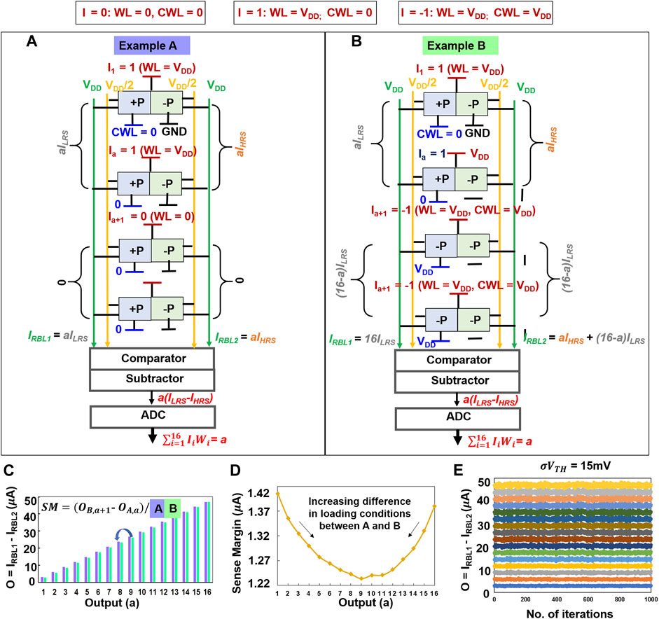
FIGURE 10. Examples of STeP-CiM for (A) best-case and (B) worst-case loading effect, (C) computation of sense margin, (D) sense margin, and (E) variation analysis for 16 activations.
The cell in row1 with I1 = 1 is in PiERRe mode. This implies that for W1 = 1, M1 is in LRS and M2 in HRS. Correspondingly, the contribution to IRBL1 and IRBL2 is ILRS and IHRS. Rows2 … 16 with I = −1 are in PiERCe. Hence, for W2 … 16 = 0 (−P, −P as per Table 3A), both M1 and M2 are in LRS (Table 2), we observe ILRS on RBL1 and RBL2. Ultimately, we obtain IRBL1 = 16ILRS and IRBL2 = IHRS+15ILRS. Overall, O1 = IRBL1−IRBL2 = ILRS−IHRS, which corresponds to output of 1. However, IRBL1 and IRBL2 in this scenario is significantly higher than example (A), reflecting worst-case loading effect.
Similarly, to obtain a MAC output of “a” while loading the RBLs maximally, “a” number of rows get input and weight as 1 (i.e., I1 … a = 1, W1 … a = 1) which contribute as IRBL1 = aILRS and IRBL2 = aIHRS. The remaining rows receive input of −1 and weight 0 (i.e., Ia+1 … 16 = −1, Wa+1 … 16 = 0). Hence, from these rows we receive IRBL1 = (16-a)ILRS and IRBL2 = (16-a)ILRS. For all the 16 rows, IRBL1 = 16ILRS and IRBL2 = 16ILRS + a(IHRS–ILRS) and Oa = a × (ILRS–IHRS) = a.
From (A) and (B), it is clear that the former and latter have highest and lowest loading effects. We take these into account while determining the maximum and minimum currents for each output (Figures 10A,B). Based on this approach, we define the worst-case sense margin for an expected output “a” (say) to be = (OMin_load,a–OMax_load,a-1)/2. Here, OMin_load,a is based on minimal loading of RBL1 and RBL2 for output “a” calculated using the method in (A), while OMax_load,a-1 is the maximum loading of RBL1 and RBL2 for the prior output “a-1” using method in (B). Figure 10B depicts this method of calculating sense margin. The calculated sense margin is plotted in Figure 10C. Note that the minimum sense margin of >1
We further perform variation analysis (Figure 10E) using Monte Carlo HSPICE simulations and analyze the sensing errors in ternary MAC based on sense margins in Figure 10D. We consider
5.4 Architecture for Increased Parallel Computation of MAC
Next, we discuss the STeP-CiM array used for performing parallel in-memory dot product computation between ternary inputs and weights. The size of our STeP-CiM array is 256 × 256 (= NR × NC). The array is segmented into 16 blocks, wherein each block consists of 16 × 256 (= NV × NC) STeP-CiM cells. All NV rows and NC columns of the block are asserted during a block access for dot product computation. Hence, a block can perform simultaneous ternary multiplication of input vector I with NV elements and weight matrix W of size NV × NC. We follow a similar architecture as proposed in (Jain et al., 2020) to compute dot product with input vectors NV > 16. In this case, partial sums are stored in a peripheral compute unit (PCU) using a sample and hold circuitry. The partial sums are accumulated after several block accesses to get the final dot product. The dot products are then quantized, and passed through an activation function to provide inputs to the next DNN layer (Jain et al., 2020). We use Q = 32 PCUs for the entire array (where Q < NC = 256) to minimize area/energy overheads of the peripheral circuits (Jain et al., 2020).
6 Results and Analysis
6.1 Array-Level Analysis
Here, we present analysis of STeP-CiM for array-level metrics, namely cell area, latency and energy for write, read and MAC operations. We compare them with near-memory designs based on PeFETs (PeFET-NM) and 2D FET based SRAM (SRAM-NM). The STeP-CiM cell presented in Figure 6A can be readily repurposed for near-memory compute by maintaining CWL = 0 V (akin to PiERRe condition), during these operations. We name this mode as PeFET-NM. Whereas, during in-memory ternary dot product computations, STeP-CiM operate with either CWL = 0 (PiERRe) for I = 1 or CWL = VDD (PiERCe) for I = −1. SRAM-NM cell is designed with two 2D FET SRAM bit cells for ternary weight storage. The 2D FETs have a feature size of 20 nm (similar to LTMD of PeFET). Consistent with PeFET based NM/STeP-CiM, VDD = 0.8 V and array size of 256 × 256 is used for SRAM-NM. For PeFET-NM and SRAM-NM, scratchpad memories are accessed row-by-row for performing vector-matrix multiplication (Jain et al., 2020). On the other hand, in STeP-CiM the same is performed by accessing 16 rows of a block simultaneously. We reiterate that the primary distinction between STeP-CiM and PeFET-NM is during compute, while they are identical for memory operations–write and read.
6.1.1 Area
We present our area analysis of STeP-CiM (or PeFET-NM) and SRAM-NM using thin-cell layout (Khare et al., 2002) based on scalable layout (
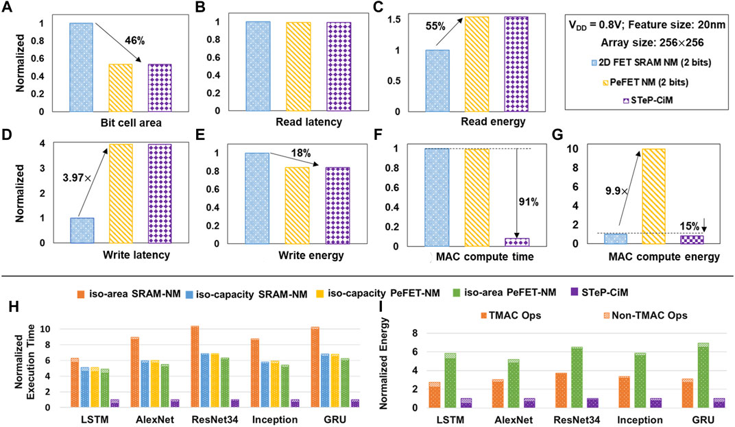
FIGURE 11. Array-level results of STeP-CiM vs. PeFET-NM and SRAM-NM shown for (A) bit cell area, (B) read latency, (C) read energy, (D) write latency, (E) write energy, (F) MAC compute time, and (G) MAC compute energy. System-level results for (H) normalized execution time. (I) Normalized energy of STeP-CiM with respect to iso-capacity and iso-area PeFET-NM and SRAM-NM.
6.1.2 Read and Write Comparisons
Performance and energy of STeP-CiM and PeFET-NM are identical since they are essentially the same bit cell during read/write operations, as also discussed earlier. Figure 11B indicates that the read latency of STeP-CiM/PeFET-NM is similar to SRAM-NM. We do not observe faster read in the former despite their compact cell area, since we must account for bit line charging time in current-based sensing mechanism employed during read. In case of SRAM-NM, where we utilize voltage-based sensing, this delay may be ignored since RBL1/RBL2 are pre-charged to VDD.
Next, we elaborate our read energy results. We calculate the read energy in Figure 11C considering active energy for 20% utilization, as reported for L2 cache by (Park et al., 2012) and leakage energy for remaining 80% utilization. The active read energy of STeP-CiM/PeFET-NM is 9× higher compared to SRAM-NM. This is because, current-based sensing in STeP-CiM/PeFET-NM necessitate switching BL1, BL2 to VDD/2 and RBL1, RBL2 to VDD during read, causing energy overheads. In case of SRAM-NM, we utilize voltage-based sensing in which BL/BLB discharge by a small voltage of 50 mV from their pre-charged state. This incurs low active read energy in SRAM-NM than in current-based sensing of STeP-CiM and PeFET-NM. However, leakage energy from the 80% idle utilization dominates in SRAM-NM, while it is insignificant in STeP-CiM/PeFET-NM. This helps reduce the read energy overhead of STeP-CiM/PeFET-NM over SRAM-NM to 55% as shown in Figure 11C.
Now, we present the write analysis. Due to polarization switching delay in STeP-CiM/PeFET-NM, they show 3.97× higher write time over SRAM-NM (Figure 11D).
Interestingly, the write energy of STeP-CiM/PeFET-NM is 18% lower than SRAM-NM (Figure 11E). Note that, similar to read, total write energy is reported considering 20% active utilization and 80% leakage in an L2 cache (Park et al., 2012). Although the active energy of STeP-CiM/PeFET-NM is 2× higher than SRAM-NM due to polarization switching, we observe benefits in total write energy due to low utilization rates of modern day caches and dominating leakage energy in SRAM-NM (Park et al., 2012). In this scenario, SRAM-NM is leaking for the remaining 80% utilization, while PeFET-NM/STeP-CiM do not, resulting in overall improvement in the latter.
6.1.3 MAC
The highlight of STeP-CiM is that we can access 16 multiple rows parallelly. On the contrary, it needs to be done sequentially in NM baselines. This property benefits both performance and energy of MAC operations using STeP-CiM. Compared to SRAM-NM, we observe ∼91% benefits in MAC latency of STeP-CiM, while PeFET-NM shows comparable latency as SRAM-NM (Figure 11F).
With respect to MAC energy in Figure 11G, STeP-CiM shows 15% improvement over SRAM-NM. Note that we obtain benefits in MAC energy with STeP-CiM because of high parallelism mentioned earlier, despite overheads of current sensing. On the contrary, Figure 11G shows overhead of MAC energy of PeFET-NM over SRAM-NM. This is attributed to high energy consumption of current-based sensing in the former compared to low energy voltage-based sensing. It is important to mention that since >90% operations in DNNs are MACs, overheads in standard read and write operations are amortized due to significant MAC benefits of the proposed STeP-CiM design. Consequently, large improvements in system performance and energy is observed in STeP-CiM, which we discuss in system-level analysis next.
6.2 System Evaluation
Here, we evaluate the system-level energy and performance benefits of CiM using STeP-CiM in five state-of-the-art DNN benchmarks, viz. AlexNet, ResNet34, Inception, LSTM and GRU.
6.2.1 Simulation Framework
We design our compute-in-memory (CiM) architecture based on TiM-DNN (Jain et al., 2020) with 32 STeP-CiM arrays, where each array consists of 256 × 256 STeP-CiM cells, providing a total memory capacity of 2 mega ternary words (512 kB). By activating 16 rows simultaneously in each of these arrays, we can perform 8196 parallel vector MAC operations with a vector length of 16. The peripheral circuitry of the STeP-CiM array consists of ADCs (Figure 9) and small compute elements to sense the MAC outputs and perform partial-sum reduction (Jain et al., 2020). We compare the STeP-CiM system with two NM baseline architectures, SRAM-NM and PeFET-NM, constructed with the corresponding memory technologies. We perform the MAC computations and partial-sum reduction in the near-memory compute (NM) units, the inputs to which are read in a sequential row-by-row manner from each memory array. We design two variants of the near-memory baseline—(i) iso-capacity and (ii) iso-area. The iso-capacity SRAM-NM and PeFET-NM baselines contain 32 memory arrays of size 512 × 256 (identical to STeP-CiM system). We design the iso-area baseline architectures with 21 SRAM-NM and 35 PeFET-NM memory arrays, each of size 512 × 256. We design the SRAM-NM iso-area baseline with a smaller number of memory arrays compared to PeFET-NM because SRAM-NM suffers area overhead due to large footprint of SRAM cell. Further, the STeP-CiM array is 1.09× larger in area compared to PeFET-NM due to the area overhead of the ADCs. We leverage the lower area of PeFET-NM to place a larger number of memory arrays compared to STeP-CiM.
6.2.2 Performance
Figure 11H shows the performance benefits of STeP-CiM over iso-capacity and iso-area SRAM-NM and PeFET-NM baselines. We obtain 6.11× and 6.13× average speed-up over the iso-capacity SRAM-NM and PeFET-NM respectively, across the benchmarks considered. Similarly, the average speed-up over iso-area SRAM-NM and PeFET-NM is 8.91× and 5.67×, respectively. The performance improvements over the near-memory baselines arise from the massively parallel in-memory MAC computation capability of STeP-CiM. The SRAM-NM and PeFET-NM iso-capacity baselines have similar performances due to similar memory read latency (discussed in the array-level results). Note that, performance enhancement of STeP-CiM over iso-area SRAM-NM is greater than over iso-capacity SRAM-NM. This is due to higher throughput of STeP-CiM than SRAM-NM at iso-area, in addition to the benefits of massively parallel MAC operations. The boosted throughput follows from the larger number of memory arrays of STeP-CiM (32 vs. 21 of SRAM-NM) available for computation at iso-area. Contrarily, the performance benefits of STeP-CiM over PeFET-NM at iso-area is slightly diminished (relative to the iso-capacity case) because PeFET-NM has a comparatively larger number of memory arrays (35 arrays of PeFET-NM compared to 32 of STeP-CiM at iso-capacity).
6.2.3 Energy
We now present the system-level energy benefits of STeP-CiM compared to near-memory baselines in Figure 11I. We note that in this evaluation, the iso-area and iso-capacity baselines are equivalent since the total energy depends on the total number operations that remain the same across these baselines. Therefore, we report the energy benefits of STeP-CiM against the iso-area baselines. We achieve 3.2× and 6.07× average energy reduction compared to iso-area/capacity SRAM-NM and PeFET-NM respectively for the benchmarks considered. The superior energy efficiency of the proposed STeP-CiM system is due to the parallelism offered by the STeP-CiM arrays as a result of multi-word line assertion for in-memory computation. PeFET-NM consumes higher energy compared to SRAM-NM because of comparatively higher read-energy caused by switching of multiple bit lines required for current-based sensing (as discussed in Section 6.1). We would like to mention here that since the bit-cell for STeP-CiM is reused for PeFET-NM, it is optimized for ternary computation rather than read.
We compare the proposed architecture with existing state-of-the-art ternary DNN accelerators in Table 4. With respect to TeC DNN (Thirumala et al., 2020) and TiM-DNN (Jain et al., 2020), we achieve 2.45× and 4.9× improvement in TOPS/W respectively. Moreover, the benefits in TOPS/mm2 are 7× and 15.15× compared to TeC DNN and TiM-DNN, respectively. The improvements are obtained due to compact size and scaled technology nodes used (20 vs. 45 nm and 32 nm) and superior compute energy efficiency. Compared to state-of-the-art GPUs, we observe up to 1486× and 5880× in TOPS/W and TOPS/mm2, respectively. Note, however, that the comparisons are made between simulation and experimental results of GPUs.

TABLE 4. System-level comparison with state-of-the-art DNNs.
7 Conclusion
In this work, we proposed a non-volatile memory (STeP-CiM) for ternary DNNs that has the ability to perform signed ternary dot product computation-in-memory. The CiM operation in our design is based on piezoelectric-induced dynamic bandgap modulation in PeFETs. We proposed a unique technique called Polarization Preserved Piezoelectric Effect Reversal with Dual Voltage Polarity (PiER) which we show is amenable for signed ternary computation-in-memory. Using this property along with multi-word line assertion, STeP-CiM performs massively parallel dot product computations between signed ternary inputs and weights. From our array-level analysis, we observed 91% lower delay and energy improvement of 15% and 91% for in-memory multiply-and-accumulate operations compared to near-memory approaches designed with 2D FET SRAM and PeFET, respectively. Our system-level evaluations show that STeP CiM achieves upto 6.13× and 8.91× average performance improvement; up to 6.07× and 3.2× reduction in energy compared to PeFET and SRAM based on near-memory baselines, respectively, across five state-of-the-art DNN benchmarks.
Data Availability Statement
The raw data supporting the conclusion of this article will be made available by the authors, without undue reservation.
Author Contributions
NT and SG conceived the idea and designed the analysis. ST contributed to the idea of current-based sensing. NT and RE used the device and array and performed system-level simulations and analyses. NT, RE, and SG wrote the manuscript. NT, RE, ST, AR, and SG analyzed the data, discussed the results, agreed on their implications, and contributed to the preparation of the manuscript. AR and SG supervised the project.
Funding
This research was supported, in part, by the Army Research Office (W911NF-19-1-048) and the SRC/NSF-funded E2CDA program (1640020).
Conflict of Interest
At the time of research, ST was a student at School of Electrical and Computer Engineering, Purdue University, USA. Presently, he is employed by Intel Corporation, USA.
The remaining authors declare that the research was conducted in the absence of any commercial or financial relationships that could be construed as a potential conflict of interest.
Publisher’s Note
All claims expressed in this article are solely those of the authors and do not necessarily represent those of their affiliated organizations, or those of the publisher, the editors, and the reviewers. Any product that may be evaluated in this article, or claim that may be made by its manufacturer, is not guaranteed or endorsed by the publisher.
References
Al Bahou, A., Karunaratne, G., Andri, R., Cavigelli, L., and Benini, L. (2018). “XNORBIN: A 95 TOp/s/W Hardware Accelerator for Binary Convolutional Neural Networks,” in IEEE Symposium on Low-Power and High-Speed Chips and Systems, COOL Chips 2018 - Proceedings (Yokohama, Japan: Institute of Electrical and Electronics Engineers Inc.), 1–3. doi:10.1109/CoolChips.2018.8373076
Alidoosty-Shahraki, M., Pourfath, M., and Esseni, D. (2019). An MoS2-Based Piezoelectric FET: A Computational Study of Material Properties and Device Design. IEEE Trans. Electron Devices 66, 1997–2003. doi:10.1109/TED.2019.2899371
Bian, Z.-J., Guo, Y., Liu, B., and Cai, H. (2021). “In-MRAM Computing Elements with Single-step Convolution and Fully Connected for BNN/TNN,” in MRAM Computing Elements with Single-step Convolution and Fully Connected for BNN/TNN. In 2021 IEEE International Conference on Integrated Circuits, Technologies and Applications, ICTA 2021 (Zhuhai, China: Institute of Electrical and Electronics Engineers Inc.), 141–142. doi:10.1109/ICTA53157.2021.9661808
Chen, W.-H., Li, K.-X., Lin, W.-Y., Hsu, K.-H., Li, P.-Y., Yang, C.-H., et al. (2018). “A 65nm 1Mb Nonvolatile Computing-In-Memory ReRAM Macro with Sub-16ns Multiply-And-Accumulate for Binary DNN AI Edge Processors,” in Digest of Technical Papers - IEEE International Solid-State Circuits Conference (San Francisco, CA, United States: Institute of Electrical and Electronics Engineers Inc.), 494–496. doi:10.1109/ISSCC.2018.8310400
Chi, P., Li, S., Xu, C., Zhang, T., Zhao, J., Liu, Y., et al. (2016). “PRIME: A Novel Processing-In-Memory Architecture for Neural Network Computation in ReRAM-Based Main Memory,” in Proceedings - 2016 43rd International Symposium on Computer Architecture, ISCA 2016 (Seoul, South Korea: Institute of Electrical and Electronics Engineers Inc.), 27–39. doi:10.1109/ISCA.2016.13
Choi, J., Wang, Z., Venkataramani, S., Chuang, P. I.-J., Srinivasan, V., and Gopalakrishnan, K. (2018). PACT: Parameterized Clipping Activation for Quantized Neural Networks. Available at: http://arxiv.org/abs/1805.06085.
Colangelo, P., Nasiri, N., Nurvitadhi, E., Mishra, A., Margala, M., and Nealis, K. (2018). “Exploration of Low Numeric Precision Deep Learning Inference Using Intel FPGAs,” in Proceedings - 26th IEEE International Symposium on Field-Programmable Custom Computing Machines, FCCM 2018 (Boulder, CO, United States: Institute of Electrical and Electronics Engineers Inc.), 73–80. doi:10.1109/FCCM.2018.00020
Courbariauxécole, M., and Bengio, Y. (2015). BinaryConnect: Training Deep Neural Networks with Binary Weights during Propagations. Montreal, Canada. doi:10.5555/2969442.2969588
Das, S. (2016). Two Dimensional Electrostrictive Field Effect Transistor (2D-EFET): A sub-60mV/decade Steep Slope Device with High on Current. Sci. Rep. 6. doi:10.1038/srep34811
Doevenspeck, J., Degraeve, R., Fantini, A., Cosemans, S., Mallik, A., Debacker, P., et al. (2021). OxRRAM-Based Analog In-Memory Computing for Deep Neural Network Inference: A Conductance Variability Study. IEEE Trans. Electron Devices 68, 2301–2305. doi:10.1109/TED.2021.3068696
Doevenspeck, J., Garello, K., Verhoef, B., Degraeve, R., van Beek, S., Crotti, D., et al. (2020). “SOT-MRAM Based Analog In-Memory Computing for DNN Inference,” in 2020 IEEE Symposium on VLSI Technology (IEEE), 1–2. doi:10.1109/VLSITechnology18217.2020.9265099
Dutta, S., Ye, H., Chakraborty, W., Luo, Y.-C., Jose, M. S., Grisafe, B., et al. (20202020). Monolithic 3D Integration of High Endurance Multi-Bit Ferroelectric FET for Accelerating Compute-In-Memory. IEEE Int. Electron Devices Meet. 36, 4.1–36.4.4. doi:10.1109/IEDM13553.2020.9371974
Hosseini, M., Elahi, M., Pourfath, M., and Esseni, D. (2015). Strain Induced Mobility Modulation in Single-Layer MoS2. J. Phys. D. Appl. Phys. 48, 375104. doi:10.1088/0022-3727/48/37/375104
Hueting, R. J. E., van Hemert, T., Kaleli, B., Wolters, R. A. M., and Schmitz, J. (2015). On Device Architectures, Subthreshold Swing, and Power Consumption of the Piezoelectric Field-Effect Transistor ( ${\pi }$ -FET). IEEE J. Electron Devices Soc. 3, 149–157. doi:10.1109/JEDS.2015.2409303
Jain, S., Gupta, S. K., and Raghunathan, A. (2020). TiM-DNN: Ternary In-Memory Accelerator for Deep Neural Networks. IEEE Trans. VLSI Syst. 28, 1567–1577. doi:10.1109/TVLSI.2020.2993045
Kazemi, A., Rajaei, R., Ni, K., Datta, S., Niemier, M., and Hu, X. S. (2020). “A Hybrid FeMFET-CMOS Analog Synapse Circuit for Neural Network Training and Inference,” in 2020 IEEE International Symposium on Circuits and Systems(IEEE), 1–5. doi:10.1109/ISCAS45731.2020.9180722
Khare, M., Ku, S. H., Donaton, R. A., Greco, S., Brodsky, C., Chen, X., et al. (2002). A High Performance 90nm SOI Technology with 0.992 μm/sup 2/6T-SRAM Cell. Tech. Dig. - Int. Electron Devices Meet., 407–410. doi:10.1109/IEDM.2002.1175865
Kim, J.-H., Jung, D. J., Kang, Y. M., Kim, H. H., Jung, W. W., Kang, J. Y., et al. (2007). “A Highly Reliable FRAM (Ferroelectric Random Access Memory),” in 2007 IEEE International Reliability Physics Symposium Proceedings. 45th Annual (IEEE), 554–557. doi:10.1109/RELPHY.2007.369950
Larsen, P. K., Kampschöer, G. L. M., Ulenaers, M. J. E., Spierings, G. A. C. M., and Cuppens, R. (1991). Nanosecond Switching of Thin Ferroelectric Films. Appl. Phys. Lett. 59, 611–613. doi:10.1063/1.105402
Lecun, Y., Bengio, Y., and Hinton, G. (2015). Deep Learning. Nature 521, 436–444. doi:10.1038/nature14539
Li, F., Zhang, B., and Liu, B. (2016). Ternary Weight Networks. Available at: http://arxiv.org/abs/1605.04711.
Li, X., Wu, J., Ni, K., George, S., Ma, K., Sampson, J., et al. (2019). Design of 2T/Cell and 3T/Cell Nonvolatile Memories with Emerging Ferroelectric FETs. IEEE Des. Test. 36, 39–45. doi:10.1109/MDAT.2019.2902094
Liao, C.-Y., Hsiang, K.-Y., Hsieh, F.-C., Chiang, S.-H., Chang, S.-H., Liu, J.-H., et al. (2021). Multibit Ferroelectric FET Based on Nonidentical Double HfZrO2 for High-Density Nonvolatile Memory. IEEE Electron Device Lett. 42, 617–620. doi:10.1109/LED.2021.3060589
Liu, Q., Gao, B., Yao, P., Wu, D., Chen, J., Pang, Y., et al. (2020). “33.2 A Fully Integrated Analog ReRAM Based 78.4TOPS/W Compute-In-Memory Chip with Fully Parallel MAC Computing,” in 2020 IEEE International Solid- State Circuits Conference - (ISSCC) (San Francisco, CA, United States: IEEE), 500–502. doi:10.1109/ISSCC19947.2020.9062953
Liu, X., Mao, M., Liu, B., Li, H., Chen, Y., Li, B., et al. (2015). “Reno,” in Proceedings - Design Automation Conference (Institute of Electrical and Electronics Engineers Inc.). doi:10.1145/2744769.2744900
Malakooti, M. H., and Sodano, H. A. (2013). Noncontact and Simultaneous Measurement of the D33 and D31 Piezoelectric Strain Coefficients. Appl. Phys. Lett. 102, 061901. doi:10.1063/1.4791573
Mishra, A., Nurvitadhi, E., Cook, J. J., and Marr, D. (2017). WRPN: Wide Reduced-Precision Networks. Available at: http://arxiv.org/abs/1709.01134.
Nayak, A. P., Bhattacharyya, S., Zhu, J., Liu, J., Wu, X., Pandey, T., et al. (2014). Pressure-induced Semiconducting to Metallic Transition in Multilayered Molybdenum Disulphide. Nat. Commun. 5. doi:10.1038/ncomms4731
Newns, D. M., Elmegreen, B. G., Liu, X.-H., and Martyna, G. J. (2012). High Response Piezoelectric and Piezoresistive Materials for Fast, Low Voltage Switching: Simulation and Theory of Transduction Physics at the Nanometer-Scale. Adv. Mat. 24, 3672–3677. doi:10.1002/adma.201104617
Ni, K., Smith, J. A., Grisafe, B., Rakshit, T., Obradovic, B., Kittl, J. A., et al. (2018). “SoC Logic Compatible Multi-Bit FeMFET Weight Cell for Neuromorphic Applications,” in 2018 IEEE International Electron Devices Meeting (IEEE), 13, 2.1–13.2.4. doi:10.1109/IEDM.2018.8614496
NVIDIA (2022). NVIDIA V100 Tensor Core. Available at: https://www.nvidia.com/en-us/data-center/v100/ (Accessed January 26, 2022).
Park, S. P., Gupta, S., Mojumder, N., Raghunathan, A., and Roy, K. (2012). “Future Cache Design Using STT MRAMs for Improved Energy Efficiency,” in Proceedings of the 49th Annual Design Automation Conference on - DAC ’12 (New York, New York, USA: ACM Press), 492. doi:10.1145/2228360.2228447
Peña-Álvarez, M., del Corro, E., Morales-García, Á., Kavan, L., Kalbac, M., and Frank, O. (2015). Single Layer Molybdenum Disulfide under Direct Out-Of-Plane Compression: Low-Stress Band-Gap Engineering. Nano Lett. 15, 3139–3146. doi:10.1021/acs.nanolett.5b00229
Rickes, J. T., Mcadams, H., Grace, J., Fong, J., Gilbert, S., Wang, A., et al. (2002). A Novel Sense-Amplifier and Plate-Line Architecture for Ferroelectric Memories. Integr. Ferroelectr. 48, 109–118. doi:10.1080/713718311
Schulman Daniel, S. (2019). Schulman Dissertation. Available at: https://www.proquest.com/docview/2432825234?pq-origsite=gscholar&fromopenview=true (Accessed March 25, 2022).
Schulman, D. S., Arnold, A. J., and Das, S. (2018). Contact Engineering for 2D Materials and Devices. Chem. Soc. Rev. 47, 3037–3058. doi:10.1039/c7cs00828g
Sebastian, A., Pendurthi, R., Choudhury, T. H., Redwing, J. M., and Das, S. (2021). Benchmarking Monolayer MoS2 and WS2 Field-Effect Transistors. Nat. Commun. 12. doi:10.1038/s41467-020-20732-w
Si, M., Cheng, H.-Y., Ando, T., Hu, G., and Ye, P. D. (2021). Overview and Outlook of Emerging Non-volatile Memories. MRS Bull. 46, 946–958. doi:10.1557/s43577-021-00204-2
Smets, Q., Groven, B., Caymax, M., Radu, I., Arutchelvan, G., Jussot, J., et al. (2019). Ultra-scaled MOCVD MoS2 MOSFETs with 42nm Contact Pitch and 250µA/µm Drain Current. IEEE Int. Electron Devices Meet. 23, 2.1–23. doi:10.1109/IEDM19573.2019.8993650
Sun, X., Yin, S., Peng, X., Liu, R., Seo, J.-s., and Yu, S. (2018). “XNOR-RRAM: A Scalable and Parallel Resistive Synaptic Architecture for Binary Neural Networks,” in Proceedings of the 2018 Design, Automation and Test in Europe Conference and Exhibition, DATE 2018 (Dresden, Germany: Institute of Electrical and Electronics Engineers Inc.), 1423–1428. doi:10.23919/DATE.2018.8342235
Suryavanshi, S. v., and Pop, E. (2016). S2DS: Physics-Based Compact Model for Circuit Simulation of Two-Dimensional Semiconductor Devices Including Non-idealities. J. Appl. Phys. 120, 224503. doi:10.1063/1.4971404
Thakuria, N., and Gupta, S. K. (2022). Piezoelectric Strain FET (PeFET) Based Non-volatile Memories. doi:10.48550/ARXIV.2203.00064
Thakuria, N., Saha, A. K., Thirumala, S. K., Schulman, D., Das, S., and Gupta, S. K. (2020a). “Polarization-induced Strain-Coupled TMD FETs (PS FETs) for Non-volatile Memory Applications,” in 2020 Device Research Conference (DRC) (IEEE), 1–2. doi:10.1109/DRC50226.2020.9135172
Thakuria, N., Schulman, D., Das, S., and Gupta, S. K. (2020b). 2-D Strain FET (2D-SFET) Based SRAMs-Part I: Device-Circuit Interactions. IEEE Trans. Electron Devices 67, 4866–4874. doi:10.1109/TED.2020.3022344
Thirumala, S. K., and Gunta, S. K. (2018). “Gate Leakage in Non-volatile Ferroelectric Transistors: Device-Circuit Implications,” in Device Research Conference - Conference Digest, DRC (Santa Barbara, CA, United States: Institute of Electrical and Electronics Engineers Inc.). doi:10.1109/DRC.2018.8442186
Thirumala, S. K., Jain, S., Gupta, S. K., and Raghunathan, A. (2020). “Ternary Compute-Enabled Memory Using Ferroelectric Transistors for Accelerating Deep Neural Networks,” in 2020 Design, Automation & Test in Europe Conference & Exhibition (DATE) (IEEE), 31–36. doi:10.23919/DATE48585.2020.9116495
Venkataramani, S., Roy, K., and Raghunathan, A. (2016). “Efficient Embedded Learning for IoT Devices,” in Proceedings of the Asia and South Pacific Design Automation Conference, ASP-DAC (Macao, China: Institute of Electrical and Electronics Engineers Inc.), 308–311. doi:10.1109/ASPDAC.2016.7428029
Wang, H., Jiang, X., Xu, N., Han, G., Hao, Y., Li, S.-S., et al. (2018a). Revised Analysis of Design Options and Minimum Subthreshold Swing in Piezoelectric FinFETs. IEEE Electron Device Lett. 39, 444–447. doi:10.1109/LED.2018.2791987
Wang, P., Xie, X., Deng, L., Li, G., Wang, D., and Xie, Y. (2018b). HitNet: Hybrid Ternary Recurrent Neural Network.
wiki chip (2012). Intel 20nm Lithography. Available at: https://en.wikichip.org/wiki/20_nm_lithography_process.
Yin, S., Jiang, Z., Seo, J.-S., and Seok, M. (2020). XNOR-SRAM: In-Memory Computing SRAM Macro for Binary/Ternary Deep Neural Networks. IEEE J. Solid-State Circuits 55, 1–11. doi:10.1109/JSSC.2019.2963616
Yoo, T., Kim, H., Chen, Q., Kim, T. T.-H., and Kim, B. (2019). “A Logic Compatible 4T Dual Embedded DRAM Array for In-Memory Computation of Deep Neural Networks,” in 2019 IEEE/ACM International Symposium on Low Power Electronics and Design (IEEE), 1–6. doi:10.1109/ISLPED.2019.8824826
Yu, S., Hur, J., Luo, Y.-C., Shim, W., Choe, G., and Wang, P. (2021). Ferroelectric HfO2-Based Synaptic Devices: Recent Trends and Prospects. Semicond. Sci. Technol. 36, 104001. doi:10.1088/1361-6641/ac1b11
Yu, Z., Ong, Z.-Y., Li, S., Xu, J.-B., Zhang, G., Zhang, Y.-W., et al. (2017). Analyzing the Carrier Mobility in Transition-Metal Dichalcogenide MoS2Field-Effect Transistors. Adv. Funct. Mat. 27, 1604093. doi:10.1002/adfm.201604093
Zhu, C., Han, S., Mao, H., and Dally, W. J. (2016). Trained Ternary Quantization. Available at: http://arxiv.org/abs/1612.01064.
Keywords: deep neural network, ferroelectric, in-memory-computing, non-volatile memory, piezoelectric, ultralow precision, strain, ternary
Citation: Thakuria N, Elangovan R, Thirumala SK, Raghunathan A and Gupta SK (2022) STeP-CiM: Strain-Enabled Ternary Precision Computation-In-Memory Based on Non-Volatile 2D Piezoelectric Transistors. Front. Nanotechnol. 4:905407. doi: 10.3389/fnano.2022.905407
Received: 27 March 2022; Accepted: 27 May 2022;
Published: 15 July 2022.
Edited by:
Catherine Schuman, The University of Tennessee, United StatesReviewed by:
Haitong Li, Stanford University, United StatesUmberto Celano, Interuniversity Microelectronics Centre (IMEC), Belgium
Copyright © 2022 Thakuria, Elangovan, Thirumala, Raghunathan and Gupta. This is an open-access article distributed under the terms of the Creative Commons Attribution License (CC BY). The use, distribution or reproduction in other forums is permitted, provided the original author(s) and the copyright owner(s) are credited and that the original publication in this journal is cited, in accordance with accepted academic practice. No use, distribution or reproduction is permitted which does not comply with these terms.
*Correspondence: Niharika Thakuria, bnRoYWt1cmlAcHVyZHVlLmVkdQ==
†Present address: Sandeep K. Thirumala, Intel Corporation, Santa Clara, CA, United States