 Akihiro Ishihara
 Godai Miyaji*
- Faculty of Engineering, Tokyo University of Agriculture and Technology, Tokyo, Japan
We report the fine periodic nanostructure formation process on metal and semiconductor surfaces in air with few-cycle 7-fs laser pulses and its physical mechanism. Using appropriate peak power densities and scanning speeds for the laser pulses, nanostructures could be formed on stainless steel and gallium arsenide (GaAs) with periods of 60–110 nm and 130–165 nm, respectively, which are 1/5–1/4 of the period of nanostructures formed with 100-fs laser pulses. The periodicity can be explained as arising from the excitation of short-range propagating surface plasmon polaritons, and the observed periods are in good agreement with the model calculation results.
1 Introduction
Multiple consecutive femtosecond (fs) laser pulses can form periodic nanostructure on dielectrics (Henyk et al., 1999; Ozkan et al., 1999; Bonse et al., 2000; Reif et al., 2002; Wu et al., 2003; Yasumaru et al., 2003), semiconductors (Borowiec and Haugen, 2003; Costache et al., 2004; Dong and Molian, 2004), and metals (Wang and Guo, 2005) with a period d much smaller than the center wavelength λ of the incident fs pulses. This is called high-spatial-frequency laser-induced periodic surface structure (HSF LIPSS) and has attracted attention as a new direct nanofabrication technique beyond the diffraction limit of light. Recently, it has been applied to functional surfaces such as those used for structural coloration (Vorobyev and Guo, 2008), anti-reflection (Yang et al., 2008), superhydrophobicity/superhydrophilicity (Wu et al., 2009), friction reduction (Yasumaru et al., 2008), and control of cell spreading (Shinonaga et al., 2015).
Studies of the physical mechanism of HSF LIPSS formation for fs laser pulses with a fluence slightly smaller than the single-shot ablation threshold have identified surface modification and roughness induced by high-density electron excitation (Miyaji and Miyazaki, 2006; Tomita et al., 2007), generation of an intense optical near-field (Miyaji and Miyazaki, 2006; Miyaji and Miyazaki, 2007; Tomita et al., 2007), and excitation of surface plasmon polaritons (SPPs) (Miyaji and Miyazaki, 2008; Miyaji et al., 2012) as dominant physical processes. In this physical picture, the surface plasmon wavelength is a key parameter that determines the period d of the nanostructure, which is roughly proportional to the wavelength of the incident light, and thus d can be shortened by using ultraviolet fs pulses (Miyaji and Miyazaki, 2016). Reducing d further requires intense ultrashort pulses with shorter wavelengths, but they are difficult to generate and handle.
Since 1999, the fundamental physical process of the photo-excited damage and ablation of the solid surfaces has been studied by using intense sub-10 fs laser pulses (Lenzner, 1999; Ganeev et al., 2013; Kafka et al., 2016). However, the HSF LIPSS formation has never been observed, while we have studied the nanostructure formation by ultrashort laser pulses. Recently, we have found that few-cycle laser pulses with a pulse duration of 7 fs and a center wavelength of 810 nm can form nanostructures with d = 60–80 nm on diamond-like carbon (DLC) films (Nikaido et al., 2018). The formation of nanostructures with d less than λ/10 (Bashir et al., 2012; Bonse et al., 2013) have been observed, while the formation mechanism has been discussed in detail. On the other hand, in the authors’ group, subsequent experiments have shown that the physical mechanism includes the generation of an ultrathin layer of high-density electrons and the excitation of short-range propagating surface plasmon polaritons (SR-SPPs) in the surrounding area (Iida et al., 2021). The SR-SPPs is one of the modes of SPPs generated at the interface between two dielectrics in contact with a thin metal film discovered by Fukui et al. (1979). Because it is a mode with large attenuation, it can propagate only in a short distance, but it is characterized by a higher wavenumber, that is, a shorter wavelength than that of SPPs excited at a single interface. For nanostructures formed with 800-nm, 100-fs laser pulses, d was observed to be ∼200 nm (Yasumaru et al., 2003), indicating that few-cycle laser pulses can form fine nanostructures without requiring wavelength conversion. However, there have been no reports on the formation of fine nanostructures on metal and semiconductor surfaces with few-cycle laser pulses, and hence details of the physical mechanism for those surfaces are unavailable.
In this study, we report the fine periodic nanostructure formation process on metal and semiconductors in air with few-cycle laser pulses, and its physical mechanism. Various peak power intensities and scanning speeds for the pulses were investigated, and nanostructures on stainless steel and gallium arsenide (GaAs) were formed with periods of 60–110 nm and 130–165 nm, respectively, which are 1/5–1/4 of the period of nanostructures formed with 100-fs laser pulses. The periodicity can be explained as arising from the excitation of short-range propagating surface plasmon polaritons. The observed period is in good agreement with the model calculation results.
2 Experimental
Figure 1 shows a schematic diagram of the optical configuration used for our ablation experiment. Linearly polarized laser pulses with a center wavelength of λ = 810 nm, pulse duration Δτ ∼ 7 fs, and repetition rate of 80 MHz were output from a Ti:sapphire laser oscillator (Novanta, Venteon Pulse One). The pulses are called few-cycle laser pulses because the number of oscillations of the electromagnetic field is only a few (Brabec and Krausz, 2000). The output pulses were passed through a pair of wedge plates with a 2-degree apex angle and a pair of chirp mirrors to compensate for the group delay dispersion of the entire optical system and maintain Δτ ∼ 7 fs The pulses were controlled with a half-wave plate and polarizer, and the polarization direction was set to horizontal. The pulses were enlarged and collimated with silver-coated curved mirrors with focal lengths of f = −50 mm and 200 mm, and focused on the target. To focus the pulses, we used a Schwarzschild reflective objective mirror (Beck Optronic Solutions, D5007-190, f = 2.6 mm, working distance WD = 1.0 mm) with a numerical aperture NA of 0.65 to prevent group delay dispersion. The focal spot and target surface were observed with a charged-coupled device (CCD) camera. The radius of the focused spot was w0 ∼ 0.4 μm at the 1/e2 value of the intensity. To confirm the pulse duration and spectrum of the pulses, a silver mirror was inserted into the beamline and the temporal and spectral profiles of the pulses were measured with spectral phase interferometry for direct electric-field reconstruction (SPIDER, APE GmbH, FC SPIDER).
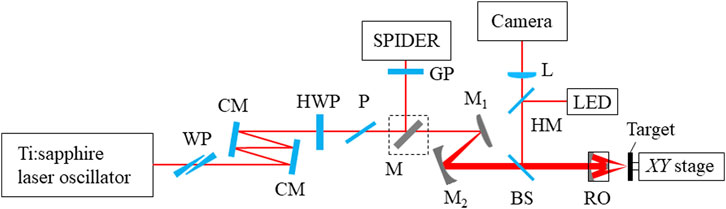
FIGURE 1. Schematic drawing of optical configuration for ablation experiment. WP: wedge plate, CM: chirp mirror, HWP: half-wave plate, P: polarizer, M: silver-coated mirror, GP: glass plate, M1: silver-coated convex mirror, M2: silver-coated concave mirror, BS: beam splitter, HM: half mirror, L: lens, RO: reflective objective mirror.
As targets, we used stainless steel (SUS304) and Si-doped, n-type (100) crystalline gallium arsenide (c-GaAs). Both targets were polished to a surface roughness of Ra < 1 nm. The targets were placed on an automated XY stage and irradiated with fs pulses, moving horizontally at a scanning speed of v = 1–10 μm/s. The peak power density was I = 2U/(πw02Δτ), where U is the pulse energy. In our ablation experiments, the SUS304 and c-GaAs surfaces were irradiated with 7-fs pulses at I = 11–21 TW/cm2 and 16–20 TW/cm2, respectively.
The target surfaces were observed using scanning electron microscopy (SEM, JEOL, JSM-6510). The spatial frequency distribution was obtained from the SEM image by a two-dimensional Fourier transform, and the period d of the nanostructure was determined from its peak frequency. Scanning probe microscopy (SPM, Shimazu, SPM-9700) was used to measure the depth of the nanostructures. In addition, the bonding structure of the stainless steel and GaAs surfaces irradiated with fs pulses was analyzed using micro-Raman spectroscopy with a diode-pumped, single-longitudinal-mode, 5-mW, 532-nm laser beam focused with a ×40 objective lens (homemade) and micro-Raman spectroscopy with a diode-pumped, single-longitudinal-mode, 5-mW, 532-nm laser beam focused with a ×100 objective lens (HORIBA, Ltd., LabRAM HR Evolution), respectively.
3 Results and discussion
3.1 Formation process of nanostructure on stainless steel
It is well known that the period d of nanostructures depends on the peak power density I and scanning speed v (i.e., the number of laser pulses N) (Yasumaru et al., 2003; Miyaji and Miyazaki, 2006). We investigated the formation process of nanostructures on SUS304 surfaces with 7-fs laser pulses, changing both I and v. Figure 2 shows SEM images of SUS304 surfaces irradiated with 7-fs pulses at I = 12.4 TW/cm2, 15.5 TW/cm2, and 20.6 TW/cm2 for v = 5 μm/s and 10 μm/s. The figure shows line-like nanostructures perpendicular to the polarization direction formed over the entire ablation trace. To make it easier to see the change in d for various I and v, d is plotted as a function of I for v = 5 μm/s and 10 μm/s in Figure 3. As I increases and v decreases (i.e., increasing N), d monotonically increases in the range d = 60–110 nm. In previous experiments, periodic nanostructures with d = 280–560 nm were formed with 800-nm, 100-fs laser pulses (Qi et al., 2009; Hou et al., 2011; Yasumaru et al., 2013; Miyazaki et al., 2015). Compared to these results, d for the 7-fs pulses is about 1/5 as large as that for the 100-fs pulses. Furthermore, the trend of increasing d with increasing I is different from that of nanostructure formation on DLC films with 7-fs pulses (Nikaido et al., 2018), while it is the same as that of nanostructure formation on SUS304 surfaces with 100-fs pulses (Qi et al., 2009; Hou et al., 2011; Yasumaru et al., 2013; Miyazaki et al., 2015). The depth of the nanostructures ranged from 10 to 40 nm and increased monotonically with increasing I.
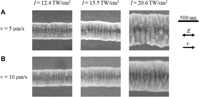
FIGURE 2. SEM images of SUS304 surfaces irradiated with 7-fs laser pulses at I = 12.4 TW/cm2, 15.5 TW/cm2, and 20.6 TW/cm2 at v = 5 μm/s (A) and 10 μm/s (B). E and v denote the directions of polarization and laser scanning, respectively.
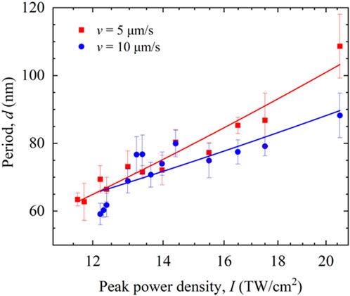
FIGURE 3. Period d of nanostructure on SUS304 formed with 7-fs pulses for scanning speeds v = 5 μm/s (red squares) and 10 μm/s (blue circles) as a function of peak power density I.
To investigate the bonding structure of SUS304 surfaces by irradiation with 7-fs pulses, we measured the Raman spectra of the irradiated surfaces. Figure 4 shows the Raman spectra of an SUS304 surface irradiated with 7-fs pulses at I = 15.5 TW/cm2 and 19.6 TW/cm2 at v = 5 μm/s and 10 μm/s. The Raman spectrum of a non-irradiated surface is also shown for comparison. The peaks at ∼690 cm−1 and ∼1,320 cm−1 indicate an A1g mode of Fe3O4 (Verble, 1974) and a second-order-longitudinal-optical (2LO) phonon mode of Fe2O3 (Ohtsuka et al., 1986; Marshall et al., 2020), respectively. At v = 5 μm/s, these peaks monotonically increased with increasing I. At v = 10 μm/s, the Fe3O4 peak was observed, while the Fe2O3 peak was small. On the other hand, the peaks of Cr2O3 [305, 348, 552, 612 cm−1 (Dostovalov et al., 2018)] were not observed in our measurement. These results indicate that a layer of iron oxide is formed on the SUS304 surface by 7-fs pulse irradiation and that the layer becomes thicker as I increases and v decreases.
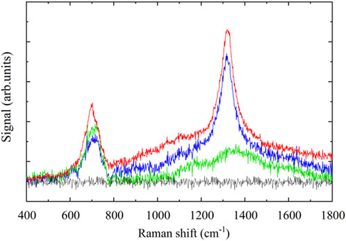
FIGURE 4. Raman spectra of SUS304 surfaces irradiated with 7-fs pulses for v = 5 μm/s at I = 15.5 TW/cm2 (blue) and 19.6 TW/cm2 (red), and for v = 10 μm/s at I = 19.6 TW/cm2 (green). The black line denotes the spectrum of a non-irradiated surface.
3.2 Formation process of nanostructure on GaAs
Figure 5 shows SEM images of GaAs surfaces irradiated with 7-fs pulses at I = 17.0 TW/cm2, 18.1 TW/cm2, and 19.6 TW/cm2 at v = 5 μm/s and 10 μm/s. The figure shows line-like nanostructures perpendicular to the polarization direction formed over the entire ablation traces. Plots of d as a function of I at v = 5 μm/s and 10 μm/s are shown in Figure 6. As I increases and v decreases (i.e., increasing N) d decreases monotonically in the range d = 130–165 nm. In previous experiments, nanostructures with d = 600–650 nm were observed to be formed with 800-nm, 100-fs laser pulses (Chakravarty et al., 2011; Ionin et al., 2013). Compared to these results, d for the 7-fs pulses was about 1/5–1/4 as large as that for the 100-fs pulses. Furthermore, the trend of increasing d with increasing I was different from that on SUS304 surfaces for 7-fs pulses. The depth of the nanostructures was in the range 30–50 nm and increased monotonically with increasing I.
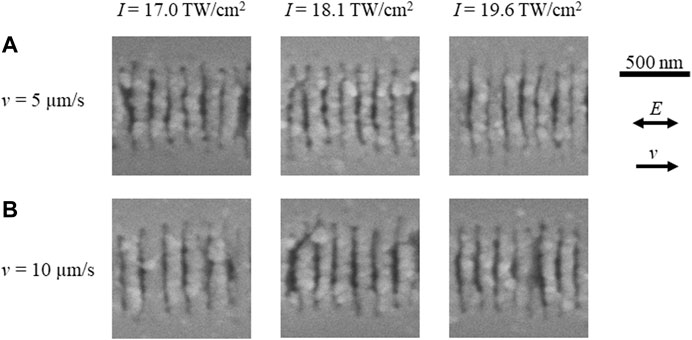
FIGURE 5. SEM images of GaAs surfaces irradiated with 7-fs laser pulses at I = 17.0 TW/cm2, 18.1 TW/cm2, and 19.6 TW/cm2 at v = 5 μm/s (A) and 10 μm/s (B). E and v denote the directions of polarization and laser scanning, respectively.
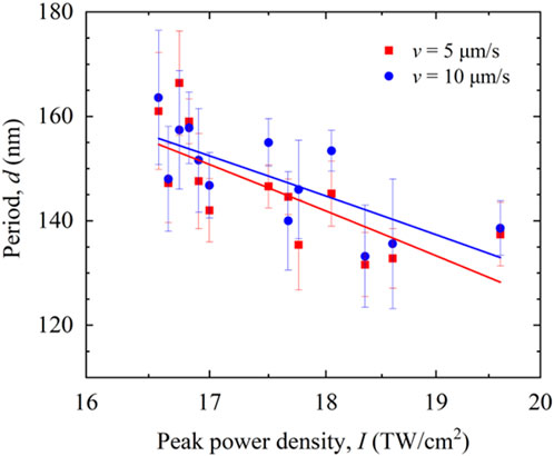
FIGURE 6. Period d of nanostructure on GaAs formed with 7-fs pulses for scanning speed v = 5 μm/s (red squares) and 10 μm/s (blue circles) as a function of peak power density I.
Figure 7 shows Raman spectra of GaAs surfaces irradiated with 7-fs pulses at I = 15.5 TW/cm2 and 19.6 TW/cm2 at v = 5 μm/s and 10 μm/s. The Raman spectrum of a non-irradiated surface is also shown for comparison. The spectrum of the non-irradiated surface contains a peak at ∼265 cm−1, ∼269 cm−1, and ∼290 cm−1, which indicates a longitudinal-optical-phonon-plasmon-coupled (LOPC) mode (Mooradian and Wright, 1966), a transverse-optical (TO) phonon mode (Abstreiter et al., 1978), and a LO phonon mode of crystalline GaAs (c-GaAs) (Abstreiter et al., 1978). The spectral peak at 290 cm−1 was reduced after laser irradiation, indicating that irradiation with multiple consecutive 7-fs pulses can change c-GaAs to amorphous GaAs (a-GaAs) (Jakata et al., 2012).
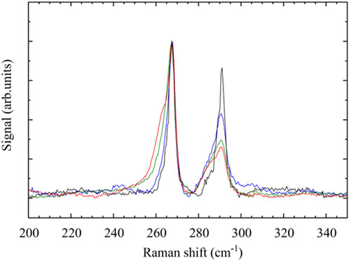
FIGURE 7. Raman spectra of GaAs surfaces irradiated with 7-fs pulses for v = 5 μm/s at I = 15.5 TW/cm2 (blue) and 19.6 TW/cm2 (red), and for v = 10 μm/s at I = 19.6 TW/cm2 (green). The black line denotes the spectrum of a non-irradiated surface.
3.3 Discussion
Based on the results obtained, we first discuss the origin of the periodicity of nanostructure formation on a SUS304 surface. In our previous report for diamond-like carbon (DLC) films, it has been shown that the few-cycle 7-fs laser pulses can form a metallic layer with a much thinner thickness (a few nm) than that with the 100-fs pulses due to the high-peak-power density of the laser pulse with low fluence and the nonlinear absorption of the target (Iida et al., 2021). It is assumed that the 7-fs pulses create a thin layer of iron oxide on the SUS304 surface, a high-density electron layer then forms in the iron oxide layer surface by large optical energy through linear and nonlinear optical absorption process (Iida et al., 2021), and SPPs are excited on the electron layer. The nanostructure can then be formed through ablation induced by the fine distribution of high-density electromagnetic energy. If the thickness of the high-density electron layer is several nanometers to several tens of nanometers, SPPs are excited at both the air/high-density electron layer and high-density electron layer/iron oxide layer interfaces and are coupled coherently. Short-range propagating SPPs (SR-SPPs) with SPP wavelength λspp = 2π/Re[kspp] can then be excited (Fukui et al., 1979; Raether, 1988). In this scenario, the following dispersion relation equation is satisfied:
where ε1, ε2, and ε3 are the dielectric constants of air, iron oxide with high-density electrons, and iron oxide, respectively, kzj2 = εj (ω/c)2 – kspp2 (j = 1, 2, 3) is the wavenumber of SPPs in each medium, and δ is the thickness of the high-density electron layer. c and ω = 2πc/λ are the speed of light in vacuum and the angular frequency, respectively. Using the Drude model (Sokolowski-Tinten and von der Linde, 2000; Danilov et al., 2015), ε2 is represented by
where εIB is the dielectric constant of unexcited iron oxide, Ne is the free electron density, Nbf is the characteristic band capacity of the specific photoexcited regions of the first Brillouin zone in the k-space associated with the band-filling effects (Danilov et al., 2015), τ is the damping time, and ωp2 = Nee2/(m*mε0) is the square of the plasma frequency with the dielectric constant of vacuum ε0, the electron mass m, and the optical relative effective mass of the electrons m*. Figure 8 shows the calculated period dcal of a nanostructure plotted as a function of electron density Ne. Since the exited SPPs are propagating in two directions along the laser polarization direction to create a standing wave mode, dcal can be λspp/2 (Novotny et al., 1997; Luo and Ishihara, 2004; Miyaji and Miyazaki, 2008). Taking ε1 = 1, we have εIB = ε3 = 6.66 + i0.29 (Karlsson and Ribbing, 1982), Nbf = 1023 cm−3 (Danilov et al., 2015), m* = 0.8 (Perevalov and Gritsenko, 2011), and τ = 1 fs (Sokolowski-Tinten and von der Linde, 2000). For comparison, we also show dcal for SPPs excited only at the interface between the iron oxide with high-density electrons and the iron oxide. In previous reports, we have shown that Ne reaches 1022 cm−3 during nanostructure formation (Miyazaki et al., 2015). In Figure 8, dcal > 30 nm can be seen for δ = 5–10 nm, while dcal increases to >60 nm as δ increases from 10 to 25 nm. For δ > 25 nm, dcal is consistent with that obtained from SPPs, which are excited only at the iron oxide with high-density electrons/iron oxide interface. As shown in our previous study by using DLC (Iida et al., 2021), the thickness of the excited layer should be shallower than the ablation depth per pulse, because SPPs could be excited on the surface having high-density electrons and their near-field could ablate the surface. Because the depth of the observed nanostructures was 10–40 nm, the thickness of the exited layer could be below these values. Based on this, dcal calculated by this model is in good agreement with the period d of the observed nanostructures. As the number of pulses irradiated per unit area increases with decreasing v, the oxide layer should become thicker and the thickness δ of the excited layer should also increase. Therefore, dcal increases with an increase in δ, as shown in Figure 8. On the other hand, an increase in I could increase both δ and Ne. The experimentally observed increase in d with an increase in I, as shown in Figure 3, indicates that the increase in dcal with increasing δ was dominant for SUS304.
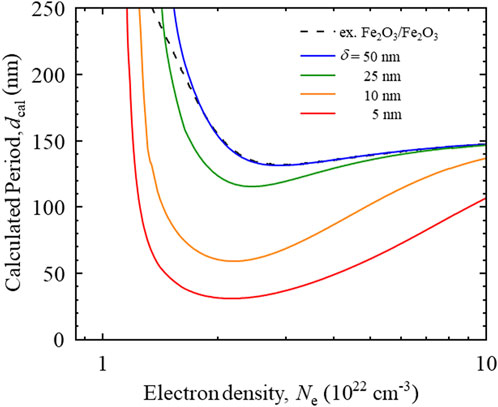
FIGURE 8. Calculated groove periods dcal as a function of electron density Ne for layer thicknesses δ = 5 nm (red), 10 nm (orange), 25 nm (green), 50 nm (blue), and λspp/2 at a single interface of excited Fe2O3/Fe2O3 (δ = ∞, dashed black).
Next, we discuss the origin of the periodicity of nanostructure formation on a GaAs surface. Assuming that the formation process of nanostructures on GaAs irradiated with 7-fs laser pulses is the same as that on stainless steel, SPPs are excited at two interfaces, air/excited a-GaAs and excited a-GaAs/c-GaAs, and are coupled coherently. Since a-GaAs has no bandgap, the bandgap renormalization effect can be neglected. Figure 9 shows dcal plotted as a function of electron density Ne, where ε1 = 1, the dielectric constant of a-GaAs εIB = 18.7 + i6.8 (Erman et al., 1984), the dielectric constant of c-GaAs ε3 = 13.55 + i0.63 (Erman et al., 1984; Palik and Palik, 1985), Nbf = 1023 cm−3 (Danilov et al., 2015), m* = 0.061 (Solymar and Walsh, 1993), and τ = 1 fs (Sokolowski-Tinten and von der Linde, 2000). For comparison, dcal is also shown for SPPs excited only at the excited a-GaAs/c-GaAs interface. In nanostructure formation on GaAs with 100-fs laser pulses with fluences of 70–200 mJ/cm2, Ne = 2.0–2.6 × 1021 cm−3 has been reported (Margiolakis et al., 2018). In Figure 9, dcal > 100 nm can be seen for δ = 5–10 nm, while dcal increases to >160 nm as δ increases from 10 nm to 25 nm. For δ > 50 nm, dcal = 120–140 nm is consistent with that obtained from SPPs excited only at the excited a-GaAs/c-GaAs interface. Because the depth of the observed nanostructures was 30–50 nm, the thickness of the exited layer could be below these values. Based on this, dcal calculated by this model is in good agreement with the period d of the observed nanostructures. As the number of pulses irradiated per unit area increases with decreasing v, the modified layer should become thicker and the thickness δ of the excited layer should also increase. Therefore, as shown in Figure 9, dcal decreases with increasing δ and Ne. This result can be well explained by the decrease in d with increasing I, as shown in Figure 6.
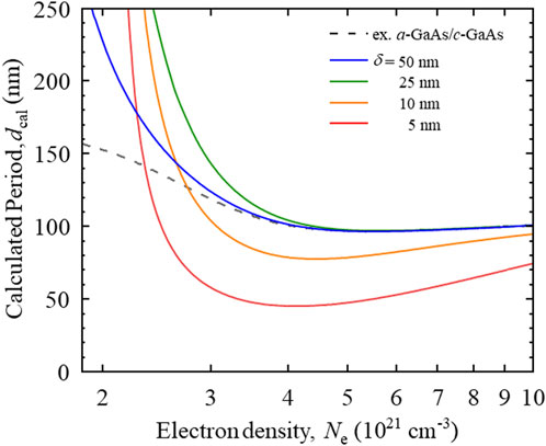
FIGURE 9. Calculated groove periods dcal as a function of electron density Ne for layer thicknesses δ = 5 nm (red), 10 nm (orange), 25 nm (green), 50 nm (blue), and λspp/2 at a single interface of excited a-GaAs/c-GaAs (δ = ∞, dashed black).
4 Conclusion
We observed the fine periodic nanostructure formation and bonding structural change on stainless steel and GaAs surfaces with 7-fs laser pulses. Experimental results showed the formation of nanostructures on SUS304 and c-GaAs with periods of 60–110 nm and 130–165 nm, respectively, which are 1/5–1/4 the period of nanostructures formed with 100-fs laser pulses. The origin of the periodicity could be explained as arising from the excitation of short-range propagating surface plasmon polaritons. The observed period is in good agreement with the model calculation results.
Data availability statement
The original contributions presented in the study are included in the article/Supplementary Material, further inquiries can be directed to the corresponding author.
Author contributions
GM designed the experiment. AI carried out the experiments. GM and AI analyzed the data and carried out the calculations. GM and AI wrote the manuscript. All authors contributed to the article and approved the submitted version.
Funding
This work is partially supported by the Amada Foundation.
Acknowledgments
The authors wish to thank Y. Iida for his helpful and useful comments on the excitation of SPPs. The measurement and analysis of the Raman spectra of the GaAs surfaces were performed at Tokyo University of Agriculture and Technology for Smart Core facility Promotion Organization. The authors thank members of Smart Core facility Promotion Organization of Tokyo University of Agriculture and Technology for technical assistance.
Conflict of interest
The authors declare that the research was conducted in the absence of any commercial or financial relationships that could be construed as a potential conflict of interest.
Publisher’s note
All claims expressed in this article are solely those of the authors and do not necessarily represent those of their affiliated organizations, or those of the publisher, the editors and the reviewers. Any product that may be evaluated in this article, or claim that may be made by its manufacturer, is not guaranteed or endorsed by the publisher.
References
Abstreiter, G., Bauser, E., Fischer, A., and Ploog, K. (1978). Raman spectroscopy—a versatile tool for characterization of thin films and heterostructures of GaAs and AlxGa1−xAs. Appl. Phys. 16, 345–352. doi:10.1007/bf00885858
Bashir, S., Rafique, M. S., and Husinsky, W. (2012). Femtosecond laser-induced subwavelength ripples on Al, Si, CaF2 and CR-39. Nucl. Instrum. Methods Phys. Res. B 275, 1–6. doi:10.1016/j.nimb.2011.12.016
Bonse, J., Sturm, H., Schmidt, D., and Kautek, W. (2000). Chemical, morphological and accumulation phenomena in ultrashort-pulse laser ablation of TiN in air. Appl. Phys. A 71, 657–665. doi:10.1007/s003390000585
Bonse, J., Höhm, S., Rosenfeld, A., and Krüger, J. (2013). Sub-100-nm laser-induced periodic surface structures upon irradiation of titanium by Ti:sapphire femtosecond laser pulses in air. Appl. Phys. A 110, 547–551. doi:10.1007/s00339-012-7140-y
Borowiec, A., and Haugen, H. K. (2003). Subwavelength ripple formation on the surfaces of compound semiconductors irradiated with femtosecond laser pulses. Appl. Phys. Lett. 82, 4462–4464. doi:10.1063/1.1586457
Brabec, T., and Krausz, F. (2000). Intense few-cycle laser fields: frontiers of nonlinear optics. Rev. Mod. Phys. 72, 545–591. doi:10.1103/revmodphys.72.545
Chakravarty, U., Ganeev, R. A., Naik, P. A., Chakera, J. A., Babu, M., and Gupta, P. D. (2011). Nano-ripple formation on different band-gap semiconductor surfaces using femtosecond pulses. J. Appl. Phys. 109, 084347/1–8. doi:10.1063/1.3580329
Costache, F., Arguirova, S. K., and Reif, J. (2004). Sub–damage–threshold femtosecond laser ablation from crystalline Si: surface nanostructures and phase transformation. Appl. Phys. A 79, 1429–1432. doi:10.1007/s00339-004-2803-y
Danilov, P. A., Ionin, A. A., Kudryashov, S. I., Makarov, S. V., Rudenko, A. A., Saltuganov, P. N., et al. (2015). Silicon as a virtual plasmonic material: acquisition of its transient optical constants and the ultrafast surface plasmon-polariton excitation. J. Exp. Theor. Phys. 120, 946–959. doi:10.1134/s1063776115050118
Dong, Y., and Molian, P. (2004). Coulomb explosion-induced formation of highly oriented nanoparticles on thin films of 3C–SiC by the femtosecond pulsed laser. Appl. Phys. Lett. 84, 10–12. doi:10.1063/1.1637948
Dostovalov, A. V., Korolkov, V. P., Okotrub, K. A., Bronnikov, K. A., and Babin, S. A. (2018). Oxide composition and period variation of thermochemical LIPSS on chromium films with different thickness. Opt. Express. 26 (6), 7712–7723. doi:10.1364/oe.26.007712
Erman, M., Theeten, J. B., Chambon, P., Kelso, S. M., and Aspnes, D. E. (1984). Optical properties and damage analysis of GaAs single crystals partly amorphized by ion implantation. J. Appl. Phys. 56, 2664–2671. doi:10.1063/1.333785
Fukui, M., So, V. C. Y., and Normandin, R. (1979). Lifetimes of surface plasmons in thin silver films. Phys. Stat. Sol. (b) 91, K61–K64. doi:10.1002/pssb.2220910159
Ganeev, R. A., Lei, D. Y., Hutchison, C., Witting, T., Frank, F., Okell, W. A., et al. (2013). Extended homogeneous nanoripple formation during interaction of high-intensity few-cycle pulses with a moving silicon wafer. Appl. Phys. A 113, 457–462. doi:10.1007/s00339-012-7430-4
Henyk, M., Vogel, N., Wolfframm, D., Tempel, A., and Reif, J. (1999). Femtosecond laser ablation from dielectric materials: comparison to arc discharge erosion. Appl. Phys. A 69, S355–S358. doi:10.1007/s003390051416
Hou, S., Huo, Y., Xiong, P., Zhang, Y., Zhang, S., Jia, T., et al. (2011). Formation of long-and short-periodic nanoripples on stainless steel irradiated by femtosecond laser pulses. J. Phys. D. Appl. Phys. 44, 505401. doi:10.1088/0022-3727/44/50/505401
Iida, Y., Nikaido, S., and Miyaji, G. (2021). Sub-100-nm periodic nanostructure formation induced by short-range surface plasmon polaritons excited with few-cycle laser pulses. J. Appl. Phys. 130, 183102/1–7. doi:10.1063/5.0069301
Ionin, A. A., Klimachev, Y. M., Kozlov, A. Y., Kudryashov, S. I., Ligachev, A. E., Makarov, S. V., et al. (2013). Direct femtosecond laser fabrication of antireflective layer on GaAs surface. Appl. Phys. B 111, 419–423. doi:10.1007/s00340-013-5350-4
Jakata, K., Wamwangi, D. M., Sumanya, C., Mathe, B. A., Erasmus, R. M., Naidoo, S. R., et al. (2012). Thermally induced amorphous to crystalline transformation of argon ion bombarded GaAs studied with surface Brillouin and Raman scattering. Nucl.Instr. Meth. 286, 25–28. doi:10.1016/j.nimb.2011.12.067
Kafka, K. R. P., Talisa, N., Tempea, G., Austin, D. R., Neacsu, C., and Chowdhury, E. A. (2016). Few-cycle pulse laser induced damage threshold determination of ultra-broadband optics. Opt. Express 24 (25), 28858–28868. doi:10.1364/oe.24.028858
Karlsson, B., and Ribbing, C. G. (1982). Optical constants and spectral selectivity of stainless steel and its oxides. J. Appl. Phys. 53, 6340–6346. doi:10.1063/1.331503
Lenzner, M. (1999). Femtosecond laser-induced damage of dielectrics. Int. J. Mod. Phys. B 13 (13), 1559–1578. doi:10.1142/s0217979299001570
Luo, X., and Ishihara, T. (2004). Surface plasmon resonant interference nanolithography technique. Appl. Phys. Lett. 84, 4780–4782. doi:10.1063/1.1760221
Margiolakis, A., Tsibidis, G. D., Dani, K. M., and Tsironis, G. P. (2018). Ultrafast dynamics and sub-wavelength periodic structure formation following irradiation of GaAs with femtosecond laser pulses. Phys. Rev. B 98, 224103–224113. doi:10.1103/physrevb.98.224103
Marshall, C. P., Dufresne, W. J. B., and Rufledt, C. J. (2020). Polarized Raman spectra of hematite and assignment of external modes. J. Raman Spectrosc. 51, 1522–1529. doi:10.1002/jrs.5824
Miyaji, G., and Miyazaki, K. (2006). Ultrafast dynamics of periodic nanostructure formation on diamondlike carbon films irradiated with femtosecond laser pulses. Appl. Phys. Lett. 89 (19), 191902/1–3. doi:10.1063/1.2374858
Miyaji, G., and Miyazaki, K. (2007). Nanoscale ablation on patterned diamondlike carbon film with femtosecond laser pulses. Appl. Phys. Lett. 91 (12), 123102/1–3. doi:10.1063/1.2784966
Miyaji, G., and Miyazaki, K. (2008). Origin of periodicity in nanostructuring on thin film surfaces ablated with femtosecond laser pulses. Opt. Express 16 (20), 16265–16271. doi:10.1364/oe.16.016265
Miyaji, G., and Miyazaki, K. (2016). Fabrication of 50-nm period gratings on GaN in air through plasmonic near-field ablation induced by ultraviolet femtosecond laser pulses. Opt. Express 24, 4648–4653. doi:10.1364/oe.24.004648
Miyaji, G., Miyazaki, K., Zhang, K., Yoshifuji, T., and Fujita, J. (2012). Mechanism of femtosecond-laser-induced periodic nanostructure formation on crystalline silicon surface immersed in water. Opt. Express 20 (14), 14848–14856. doi:10.1364/oe.20.014848
Miyazaki, K., Miyaji, G., and Inoue, T. (2015). Nanograting formation on metals in air with interfering femtosecond laser pulses. Appl. Phys. Lett. 107, 071103/1-5. doi:10.1063/1.4928670
Mooradian, A., and Wright, G. B. (1966). Observation of the interaction of plasmons with longitudinal optical phonons in GaAs. Phy. Rev. Lett. 16 (22), 999–1001. doi:10.1103/physrevlett.16.999
Nikaido, S., Natori, T., Saito, R., and Miyaji, G. (2018). Nanostructure Formation on diamond-like carbon films induced with few-cycle laser pulses at low fluence from a Ti:sapphire laser oscillator. Nanomaterials 8, 535. doi:10.3390/nano8070535
Novotny, L., Hecht, B., and Pohl, D. W. (1997). Interference of locally excited surface plasmons. J. Appl. Phys. 81, 1798–1806. doi:10.1063/1.364036
Ohtsuka, T., Kubo, K., and Sato, N. (1986). Raman spectroscopy of thin corrosion films on iron at 100 to 150 C in air. Corrosion 42 (8), 476–481. doi:10.5006/1.3583054
Ozkan, A. M., Malshe, A. P., Railkar, T. A., Brown, W. D., Shirk, M. D., and Molian, P. A. (1999). Femtosecond laser-induced periodic structure writing on diamond crystals and microclusters. Appl. Phys. Lett. 75, 3716–3718. doi:10.1063/1.125439
Palik, E. D. (1985). in Handbook of optical constants of solids. Editor E. D. Palik (London: Academic), 429–443.
Perevalov, T. V., and Gritsenko, V. A. (2011). Electronic structure of TiO2 rutile with oxygen vacancies: ab initio simulations and comparison with the experiment. J. Exp. Theor. Phys. 112, 310–316. doi:10.1134/s1063776111010158
Qi, L., Nishii, K., and Namba, Y. (2009). Regular subwavelength surface structures induced by femtosecond laser pulses on stainless steel. Opt. Lett. 34, 1846–1848. doi:10.1364/ol.34.001846
Raether, H. (1988). Surface plasmons on smooth and rough surfaces and on gratings. Berlin: Springer-Verlag, 24–29.
Reif, J., Costache, F., Henyk, M., and Pandelov, S. V. (2002). Ripples revisited: non-classical morphology at the bottom of femtosecond laser ablation craters in transparent dielectrics. Appl. Surf. Sci. 197-198, 891–895. doi:10.1016/s0169-4332(02)00450-6
Shinonaga, T., Tsukamoto, M., Kawa, T., Chen, P., Nagai, A., and Hanawa, T. (2015). Formation of periodic nanostructures using a femtosecond laser to control cell spreading on titanium. Appl. Phys. B 119, 493–496. doi:10.1007/s00340-015-6082-4
Sokolowski-Tinten, K., and von der Linde, D. (2000). Generation of dense electron-hole plasmas in silicon. Phys. Rev. B - Condens. Matter Mater Phys. 61, 2643–2650. doi:10.1103/physrevb.61.2643
Solymar, L., and Walsh, D. (1993). Lectures on the electrical properties of materials. Oxford: Oxford Science Publications, 191.
Tomita, T., Kinoshita, K., Matsuo, S., and Hashimoto, S. (2007). Effect of surface roughening on femtosecond laser-induced ripple structures. Appl. Phys. Lett. 90, 153115/1–3. doi:10.1063/1.2720709
Verble, J. L. (1974). Temperature-dependent light-scattering studies of the Verwey transition and electronic disorder in magnetite. Phys. Rev. B 9 (12), 5236–5248. doi:10.1103/physrevb.9.5236
Vorobyev, A. Y., and Guo, C. (2008). Colorizing metals with femtosecond laser pulses. Appl. Phys. Lett. 92, 041914. doi:10.1063/1.2834902
Wang, J., and Guo, C. (2005). Ultrafast dynamics of femtosecond laser-induced periodic surface pattern formation on metals. Appl. Phys. Lett. 87, 251914/1–3. doi:10.1063/1.2146067
Wu, Q., Ma, Y., Fang, R., Liao, Y., Yu, Q., Chen, X., et al. (2003). Femtosecond laser-induced periodic surface structure on diamond film. Appl. Phys. Lett. 82, 1703–1705. doi:10.1063/1.1561581
Wu, B., Zhou, M., Li, J., Ye, X., Li, G., and Cai, L. (2009). Superhydrophobic surfaces fabricated by microstructuring of stainless steel using a femtosecond laser. Appl. Surf. Sci. 256, 61–66. doi:10.1016/j.apsusc.2009.07.061
Yang, Y., Yang, J., Liang, C., and Wang, H. (2008). Ultra-broadband enhanced absorption of metal surfaces structured by femtosecond laser pulses. Opt. Express 16, 11259–11265. doi:10.1364/oe.16.011259
Yasumaru, N., Miyazaki, K., and Kiuchi, J. (2003). Femtosecond-laser-induced nanostructure formed on hard thin films of TiN and DLC. Appl. Phys. A 76, 983–985. doi:10.1007/s00339-002-1979-2
Yasumaru, N., Miyazaki, K., and Kiuchi, J. (2008). Control of tribological properties of diamond-like carbon films with femtosecond-laser-induced nanostructuring. Appl. Surf. Sci. 254, 2364–2368. doi:10.1016/j.apsusc.2007.09.037
Keywords: femtosecond laser, laser material processing, surface plasmon polariton, stainless steel, gallium arsenide
Citation: Ishihara A and Miyaji G (2023) Fine periodic nanostructure formation on stainless steel and gallium arsenide with few-cycle 7-fs laser pulses. Front. Nanotechnol. 5:1249648. doi: 10.3389/fnano.2023.1249648
Received: 29 June 2023; Accepted: 08 September 2023;
Published: 19 September 2023.
Edited by:
Koji Sugioka, RIKEN, JapanReviewed by:
George Tsibidis, Foundation for Research and Technology Hellas, GreeceSergey Kudryashov, The Russian Academy of Sciences (RAS), Russia
Copyright © 2023 Ishihara and Miyaji. This is an open-access article distributed under the terms of the Creative Commons Attribution License (CC BY). The use, distribution or reproduction in other forums is permitted, provided the original author(s) and the copyright owner(s) are credited and that the original publication in this journal is cited, in accordance with accepted academic practice. No use, distribution or reproduction is permitted which does not comply with these terms.
*Correspondence: Godai Miyaji, Z21peWFqaUBjYy50dWF0LmFjLmpw