 N. Schmitt
 A. Ascoli
 I. Messaris
 A. S. Demirkol
 S. Menzel
 V. Rana
 R. Tetzlaff
 L. O. Chua
- 1Institute of Circuits and Systems, Faculty of Electrical and Computer Engineering, Technische Universität Dresden, Dresden, Germany
- 2Department of Electronics and Telecommunications, Politecnico di Torino, Turin, Italy
- 3Peter Grünberg Institut 7, Forschungszentrum Jülich GmbH, Jülich, Germany
- 4Peter Grünberg Institut 10, Forschungszentrum Jülich GmbH, Jülich, Germany
- 5Department of Electrical Engineering and Computer Sciences, University of California, Berkeley, Berkeley, CA, United States
Fading memory is the capability of a physical system to approach a unique asymptotic behaviour, irrespective of the initial conditions, when stimulated by an input from a certain class. Standard stimuli from the AC periodic class typically induce fading memory effects in non-volatile memristors, as uncovered for the first time back in 2016. Very recently, a deep investigation of resistance switching phenomena in a TaOx resistive random access memory cell revealed the capability of the nano-device to exhibit one of two possible oscillatory behaviours, depending upon the initial condition, when subject to a particular periodic excitation. This interesting finding was, however, left unexplained. Bistability is the simplest form of local fading memory. In a system, endowed with local fading memory under a given stimulus, the initial condition does not affect the long-term behaviour of the state as long as it is drawn from the basin of attraction of either of the distinct coexisting state-space attractors (two limit cycles for the periodically forced memristor acting as a bistable oscillator). Here, the history of the system, encoded in the initial condition, is, thus, erasable only locally through ad hoc stimulation. Motivated by the discovery of local history erase effects in our resistive random access memory cell, this study applies a powerful system-theoretic tool, enabling the analysis of the response of first-order systems to square pulse train-based periodic stimuli, known as the time-average state dynamic route, to an accurate physics-based mathematical model, earlier fitted to the nano-device, to determine a strategy for specifying the parameters of an excitation signal, consisting of the sequence of two square pulses of opposite polarity per period so as to induce various forms of monostability or multistability in the non-volatile memristor. In particular, as an absolute novelty in the literature, experimental measurements validate the theoretical prediction on the capability of the device to operate as one of two distinct oscillators, depending upon the initial condition, under a specific pulse train excitation signal. The coexistence of multiple oscillatory operating modes in the periodically forced resistive random access memory cell, an example par excellence of their unique non-linear dynamics, may inspire the development and circuit implementation of novel sensing and mem-computing paradigms.
1 Introduction
Resistance switching memories (Ielmini and Waser, 2016), falling in the class of non-volatile memristors (Chua, 2018), are currently under the zooming lens of thousands of researchers worldwide (Buckwell et al., 2021; Shamsi et al., 2021; Milano et al., 2022; Lenk et al., 2023; Tzouvadaki et al., 2023) for the wide spectrum of opportunities they open up in the post-Moore electronics era (Yi et al., 2022). In addition to their obvious use as data storage units, memristors from the non-volatile class (Mikolajick et al., 2009; Vontobel et al., 2009) may be alternatively operated as data processing elements, enabling the circuit implementation of innovative in-memory computing paradigms (Xia and Yang, 2019), which promise to resolve the von Neumann bottleneck, limiting the performance of state-of-the-art computers, in which the central processing unit is frequently forced to remain in an idle state, preventing its potential to be fully harnessed, to enable relevant data transfer across the physical channel, which allows its communication with the physically separated memory. Furthermore, their typical arrangement within dense crossbar arrays, whose design exploits the need to introduce thin oxide films for isolation purposes between adjacent metal layers in standard CMOS fabrication processes, favours the development of hardware engines, which leverage state-dependent Ohm's law-based electronic transport in the nano-device to accelerate matrix-vector multiplications (Hu et al., 2016), lying at the core of most machine learning algorithms for Big Data analysis nowadays. Despite the considerable progress, achieved over the past 15 years through the pursuit of significant research studies (Waser and Aono, 2007; Valov et al., 2013; Wang et al., 2017; Rao et al., 2023) aimed to understand the fundamentals of the operating mechanisms of resistance switching memories, some aspects of the intricate, yet peculiar, non-linear dynamics (Corinto et al., 2015) of these devices, of potential interest for electronic applications (Talati et al., 2016; Sebastian et al., 2017; Di Ventra and Traversa, 2018; Li et al., 2018; Zidan et al., 2018), are yet to be discovered. Back in 2016, the theoretical analysis of a predictive mathematical model by Strachan et al. (2013) first unveiled the emergence of memory loss phenomena (Ascoli et al., 2017), coexisting with analogue non-volatility, in a TaOx resistive random access memory (ReRAM) device under suitable periodic excitation. As confirmed shortly later in laboratory measurements, carried out on a physical sample at Hewlett Packard Labs (Ascoli et al., 2016c), the initial condition was found to have no impact on the asymptotic oscillatory behaviour of the periodically driven non-volatile memory device. History erase effects were found to appear across this memristor physical realization under a wide class of periodic stimuli, typically employed in electrical engineering, including triangular, square, and sine waves. The ubiquity of this non-linear dynamic phenomenon in non-volatile memristors was further revealed shortly later (Menzel et al., 2017; Ascoli et al., 2018). The fading memory phenomenon originates in real non-volatile memristor devices due to the intrinsic asymmetry in their SET and RESET switching kinetics. In fact, constructing artificially a device model with symmetric ON and OFF dynamics, as is the case for ideal memristors, no history erase effect would be observed, irrespective of the stimulus. In these circumstances, the periodically forced device would be found to exhibit an initial condition-dependent oscillatory behaviour directly from the beginning of the AC stress test. On the other hand, in general, a physical memristor realisation, under periodic excitation, undergoes transient phenomena, before locking into some oscillatory operating mode, whereby the effect of SET and RESET forces on its kinetics balances out over each input cycle. In system theory, a physical system, which exhibits a unique asymptotic behaviour under a given stimulus, is said to have fading memory (Boyd and Chua, 1985) on that stimulus. A local form of fading memory was introduced theoretically in Ascoli et al. (2016a) to define the capability of a physical system to lock into one of a number of distinct operating modes under a given excitation, depending upon the initial condition. A physical system of this kind is said to undergo fading memory effects locally within the basin of attraction of each of the locally stable attractors in the associated state space. Although a memristive circuit, employing standard electrical components, including active components, was designed in Ascoli et al. (2016b) to provide a pedagogical example of a physical system, endowed with local fading memory on a given input class, no physical memristor realisation was ever found to experience input-induced multistability until recent observations of bistability in the oscillatory behaviour of the state of the Strachan model under suitable pulse train-based excitation, as reported in an interesting bifurcation study from Pershin and Slipko (2019). A comprehensive theoretico-experimental research study (Ascoli et al., 2022), allowing to gain a deep insight into the mechanisms, underlying resistance switching phenomena in another ReRAM cell—composed of a Ta/TaOx/Pt device stack—and manufactured at the premises of Forschungszentrum Jlich (FZJ), similarly reported the coexistence of two stable oscillatory solutions for the dimensionless memory state x of the associated physics-based mathematical description (Hardtdegen et al., 2018), known as the Jülich Aachen resistive switching tool (JART) valence change memory (VCM) model (Bengel et al., 2022), preliminarily fitted to experimental data, extracted from a device sample, under a particular symmetric periodic triangular stimulus. The device was found to operate around its fully-RESET state in one of the two oscillatory operating modes. The research work, presented in this manuscript, intends to answer key questions, which emerged from this observation, as listed here.
1. Is it possible to elucidate the mechanisms behind the emergence of bistability in the oscillatory response of our ReRAM cell under suitable periodic stimulation, as reported yet left unexplained in Ascoli et al. (2022)?
2. Is it possible to excite the nano-device in such a way that it may feature a larger number of coexisting oscillatory operating modes?
3. Is it possible to modulate the excitation signal in such a way to switch the nature of the device oscillatory response from unimodal to multimodal, or vice versa?
4. Is there a quantitative measure for identifying each possible asymptotic oscillatory steady state for the device, subject to a given periodic stimulus, from the analysis of the competition between the counteractive forces, acting on the device kinetics, under SET and RESET phases over each cycle?
5. Is it possible to develop a rigorous methodology to tailor the shape of the periodic stimulus in such a way to induce a variable number of stable oscillatory operating modes into the device?
6. Is it possible to demonstrate experimentally the emergence of the simplest form of local fading memory in a non-volatile memristor?
In order to address these points, a powerful system-theoretic graphic tool, known as the time-average state dynamic route (TA-SDR), inspired from the bifurcation study in Pershin and Slipko (2019), exploiting the time-averaging method from the theory of non-linear dynamics (Guckenheimer and Holmes, 1983), is applied to the JART VCM model to derive a systematic technique for massaging the properties of two square pulses of opposite polarity, composing the train-based stimulus over each cycle, for inducing monostability or multistability in the oscillatory response of the TaOx ReRAM nano-device manufactured in house. For one particular input parameter setting, the predictions from the proposed theory are validated experimentally in our laboratory facilities, strengthening the significance of our research findings. In regard to the structure of this paper, the motivation behind our research work is elucidated in Section 2. The TA-SDR technique, extending the dynamic route map (DRM) concept (Chua, 2018) to enable the analysis of the time evolution of the mean value of the memory state of a first-order dynamical system under square pulse train stimulation, in those circumstances where the memory state undergoes small changes per cycle, which is the case, for example, in high-frequency excitation scenarios (Messaris et al., 2023), is introduced in Section 3. Section 4 presents a rigorous methodology, based upon the TA-SDR tool, allowing to determine appropriate heights and widths for the two pulses, composing the train stimulus over each cycle so as to endow the time-average state equation (TA-SE), governing the dynamics of the mean value
2 Motivation
The TaOx ReRAM cell, under focus in this research study, is a voltage-controlled VCM device. The voltage v (current i) across (through) its physical stack then acts as the input (output) variable for the associated memristor model. The differential algebraic equation (DAE) set of the JART VCM model, which captures very accurately the device dynamics and is the object of the theoretical analysis to follow, may be numerically cast, as explained in Supplementary Appendix A.1, in the characteristic form of a first-order voltage-controlled extended memristor, i.e.,
where the ordinary differential equation (ODE) (Eq. 1), known as the state equation (SE), governs the time evolution of a dimensionless memory state x, constrained to lie at all times within a closed set
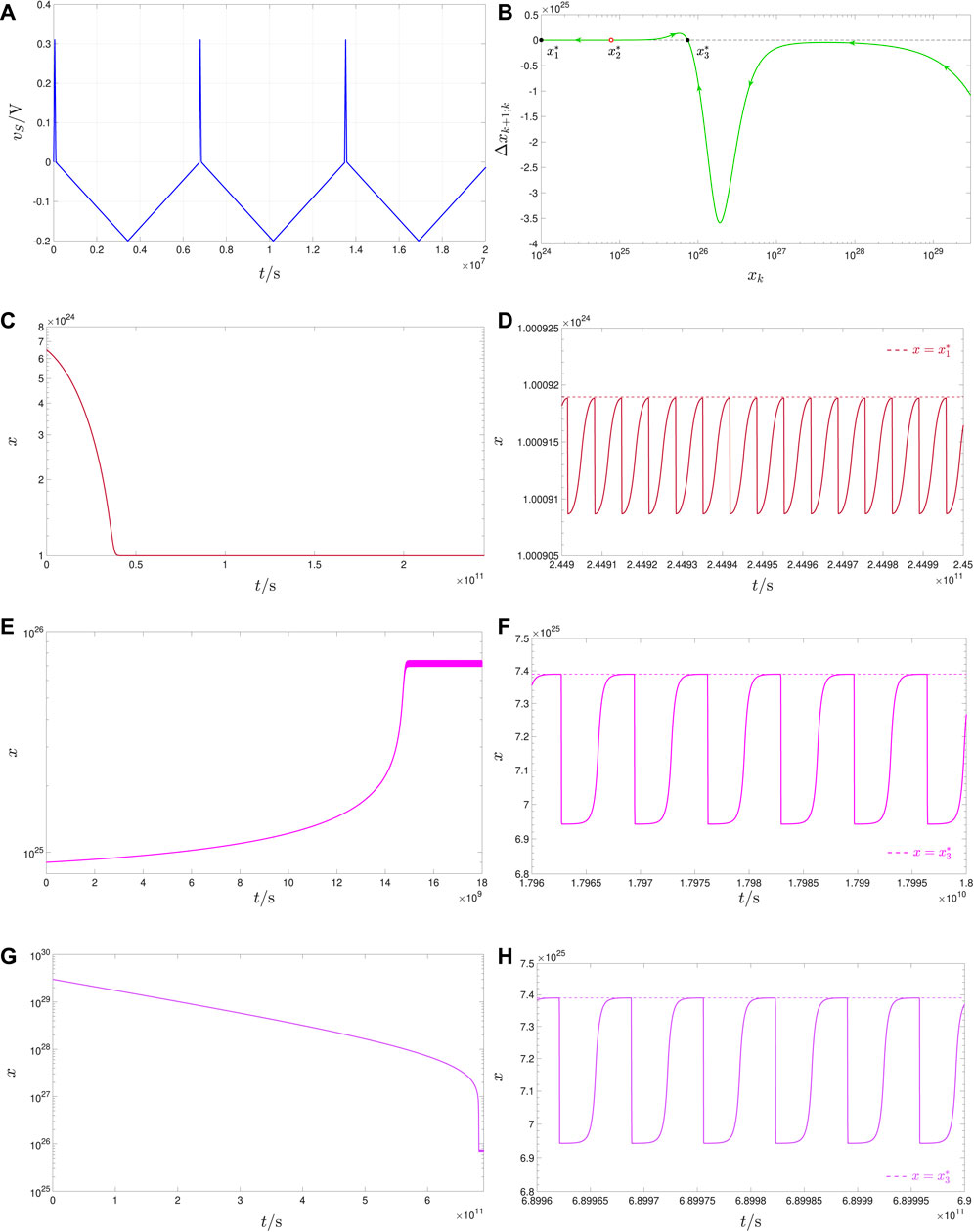
Figure 1. (A) Time waveform of an asymmetric periodic triangular voltage stimulus vS, which, according to the JART VCM model predictions, induces bistable steady-state oscillatory dynamics in the TaOx ReRAM cell, manufactured in Jülich, as it falls continuously between its terminals. The amplitude V+ (V−) and width τ+ (τ−) of the positive RESET (negative SET) triangular pulse over each input cycle are, respectively, set to 0.31 V (−0.2 V) and 1 ⋅ 105s (6.6667 ⋅ 106s). The period T of the stimulus is then τ+ + τ− = 6.7667 ⋅ 106s. The reset–set pulse width ratio r ≜ τ+/τ− amounts here to 1.5 ⋅ 10–2. (B) Δxk+1;k versus xk locus (Ascoli et al., 2023b), as extracted from the Poincaré map
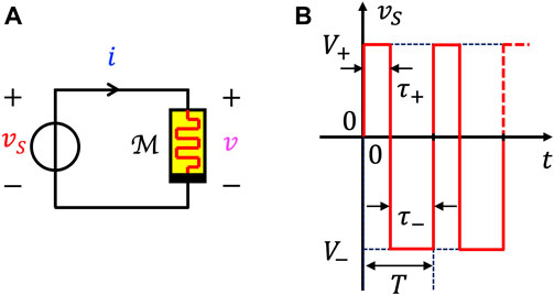
Figure 2. (A) Circuit setup for investigating the response of a voltage-controlled memristor
Remark 1. Let us consider a first-order ODE system, falling in the class (Eq. 1), where x is a scalar state with the existence domain
Here, the Poincaré map admits a triplet of fixed points, specifically
3 The TA-SDR: a system-theoretic tool for the study of the response of first-order memristors to square pulse train stimuli
This section describes a powerful graphic method, which allows investigating the response of first-order nonlinear dynamical systems to AC periodic square pulse train-based excitations. It was introduced and applied to the Strachan model from Strachan et al. (2013) in an interesting numerico-analytical study (Pershin and Slipko, 2019) of the bifurcations, experienced by the TaOx ReRAM cell, manufactured at Hewlett Packard Labs, under periodic stimuli of this kind, and later employed in a deep study (Messaris et al., 2023) of the high-frequency response of the same nano-device.
Without loss of generality, consider the DAE SET (Eqs 1, 2) of an extended first-order voltage-controlled memristor (Chua, 2018). The JART VCM model, revisited in Supplementary Appendix A.1, may be formulated in this form. An AC voltage source vS is now inserted across the memristor
Applying the Leibniz integral rule to Eq. 3, the time derivative of the time average state varies with time as
Now, integrating the state Eq. 1 over a period gives the following expression:
in which the last line assumes that within the time duration of a RESET (SET) pulse, the memory state undergoes7 such a small decrease (increase) to justify its approximation via the respective time average, within the argument of the state evolution function in the first (second) time integral, without introducing a noticeable loss in computation accuracy. Finally, substituting Eq. 6 into Eq. 4 allows deriving the TA-SE, specifically
which8 governs the time evolution of the time average state
An equilibrium
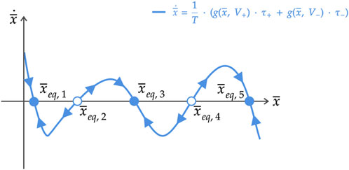
Figure 3. Exemplary illustration for the TA-SDR of a first-order memristor under periodic stimulation, as established in the test circuit of Figure 2A, from an AC voltage source vS, generating a specific periodic square pulse train, of the kind shown in plot (b) of the same figure. Each filled (hollow) circle along the horizontal axis indicates an asymptotically stable (an unstable) equilibrium
In the next section, a rigorous methodology, based upon the system-theoretic TA-SDR analysis tool, shall be set in place to massage the four parameters of the AC periodic pulse train stimulus of Figure 2B in such a way to induce the coexistence of a variable number of distinct steady-state oscillatory solutions for the memory state of the ReRAM cell under the zooming lens in this manuscript.
4 A systematic technique to endow the periodically driven memory cell with a variable number of oscillatory operating modes
Let us commence this section by introducing an alternative way to determine the equilibria of TA-SE and study their local stability properties.
4.1 TA-SDR decomposition
The TA-SE (Eq. 7) can be recast as the sum between a RESET component and a SET component via
The first and latter contributions are, respectively, defined as
The RESET (SET) component is, in fact, a scaled version of the right hand side of the SE9 (Eq. 1), with the time-average state in place for the state, under a positive (negative) DC voltage V = V+ (V−). As an exemplary case study, the RESET and SET components, whose sum results in TA-SDR, illustrated in Figure 3, are, respectively, shown through a solid red and blue trace as a function of the time-average state in Figure 4A. Arrows along the first (latter) component point toward the west (the east), revealing that the physics laws, governing the OFF (ON) dynamics, establish a decrease (an increase) for the time-average state over the time interval τ+ (τ−), when the positive (negative) square pulse of height V+ (V−) perturbs the memristor. Far more insightful is the illustration of Figure 4B, showing the moduli of the RESET and SET components from plot (a) of the same figure. Note that in this new graphic representation, the direction of motion for the time-average state along the RESET (SET) trace still takes into account the negative (positive) polarity of the contribution expressed by Eqs 9, 10. Naturally, the TA-SE, cast as reported in Eq. 8, admits an equilibrium
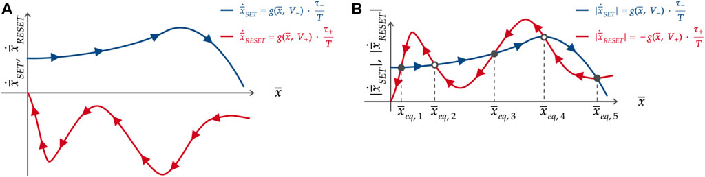
Figure 4. (A) Decomposition of the exemplary TA-SDR from Figure 3 into its two constitutive contributions, referred to as RESET and SET components, which are, respectively associated with the positive and negative square pulse, composing the time waveform of a given ReRAM cell stimulus, falling in the class from Figure 2B, over the first (second) τ+ (τ−)-long part of each cycle. The RESET (SET) component lies on the lower (upper) half of the
Moreover, the equilibrium is asymptotically stable if and only if the ON (OFF) dynamics are dominant over the OFF (ON) dynamics to its left (right). The decomposition of the TA-SE into its SET and RESET components is at the basis of a systematic methodology to craft the periodic pulse train stimulus, to be applied across the nano-device, so as to endow its memory state with oscillatory monostable or multistable response, as elucidated in Section 4.3. Before presenting the methodology, it is worth exploring the state evolution function g (x, v) versus state x loci under sweep in the positive (negative) DC value V+ (V−), assigned to the input variable to the ODE (Eq. 1). In fact, the larger the difference between the shapes of the SET SDRs and the shapes of the RESET SDRS and the higher the tunability of the loci within each of these two families, the simpler would be to modulate the two components of the TA-SE so as to enforce a desired number of intersections between the graphs of their moduli along the state existence domain.
4.2 Impact of the positive/negative DC voltage on the shape of the ReRAM cell RESET/SET SDR
The TA-SE (Eq. 7), corresponding to a given square pulse train excitation, is a linear combination of two copies of the state evolution function. The first (latter) copy is expressed in terms of the time-average state and of the positive (negative) DC voltage, representing the height of the first RESET (second SET) pulse in the waveform of the AC periodic input over each cycle, and is weighted by the ratio between the width of the same pulse and the period of the stimulus. Moreover, the intersections between the loci of the moduli of these two terms identify the admissible equilibria for the TA-SE. In order to develop a strategy to endow the TA-SE with a desired number of stable equilibria, falling within the memory state existence domain, it is of interest to explore the influence of the positive (negative) value V+(V−), assigned to a DC voltage V, employed within the argument of the state evolution function, on the shape of the RESET (SET) SDR. Plots (a), (c), (e), and (g) ((b), (d), (f), and (h)) of Figure 5, respectively, show the RESET (SET) SDR associated with the first, second, third, and fourth V+ (V−) values from the set {+(−)0.2, + (−)0.4, + (−)0.6, + (−)0.8}V. A couple of important points stand out from the graphical inspection of these plots. First, differently from what is the case for other ReRAM cells (Ascoli et al., 2023a), the shapes of the loci, associated with positive-valued DC stimuli, do not differ so significantly from those, associated with negative-valued DC stimuli, complicating the identification of a simple strategy to vary the number of crossings between the moduli of the loci of the SET and RESET TA-SE components. Second, as established by the boundary conditions, included in the JART VCM model, which is reviewed in Supplementary Appendix A.1, while the memory state approaches the lower (upper) bound in its existence domain during a RESET (SET) transition, its deceleration is rather abrupt, as demonstrated by the sudden fall of either locus on the left (right) column of plots in Figure 5 in the neighbourhood of the minimum (maximum) allowable state value. On the other hand, the memory state does not accelerate (decelerate) in a similarly dramatic way as it increases (decreases) from values close to the lower (upper) bound in its existence domain over the course of a SET (RESET) process, as revealed by the relatively mild ascent (descent) of either locus on the right (left) column of plots in Figure 5 in the neighbourhood of the minimum (maximum) allowable state value. The rather different behaviour of the SET and RESET SDRs around the lower (upper) bound in the state existence domain explains why it is relatively simple to choose the stimulus parameters, namely, V+, τ+, V−, and τ−, in such a way to enforce one intersection between the loci of the moduli of the SET and RESET TA-SE components in the vicinity of the smallest (highest) admissible state value. Massaging conveniently the four input parameters, it is further possible to ensure that the modulus of the RESET (SET) term in the linear combination on the right hand side of the TA-SE is larger than the modulus of the other SET (RESET) term to the right (left) of the lower (upper) bound in the state existence domain, which ensures that the solution to the ODE (Eq. 1) would exhibit a steady-state oscillatory waveform around the fully-RESET (fully-SET) state, as revealed, for example, in the monostability case study 1.1 (1.4) from Section 5.1.1 (5.1.4). However, it is fair to admit that, in an excitation scenario from the first (latter) kind, the ReRAM cell typically exhibits slower and slower dynamics as the respective memory state gets closer and closer to its minimum (maximum) allowable value. Therefore, the practical exploitation of a device oscillatory mode, implying the excursion of the memory state around a level in the proximity of the lower (upper) bound in its existence domain, is questionable. Moreover, in general, it is advisable to operate the device away from its fully-RESET (fully-SET) state. Far more interesting, yet harder, is to craft the square pulse train stimulus in such a way to induce the asymptotic emergence of at least one oscillatory state solution unaffected by the boundary conditions, and thus undergoing a periodic excursion across a real-valued range, falling well within its admissible existence domain, as shown, for example, in the multistability case study 1.2 (1.3) from Section 5.1.2 (5.1.3), where, taking into account that stable and unstable equilibria of a TA-SE alternate one after the other, as shown in the representative illustration of Figure 3, the moduli of the loci of the SET and RESET TA-SE components are enforced to feature as many as three (five) crossings, in order for the solution to the state Eq. 1 to exhibit a bistable (tristable) oscillatory behaviour after transients decay to zero. The next section presents a rigorous strategy to shape the AC periodic square pulse train input, applied to the JART VCM model, in such a way to endow its state variable with a monomodal or multimodal oscillatory response.
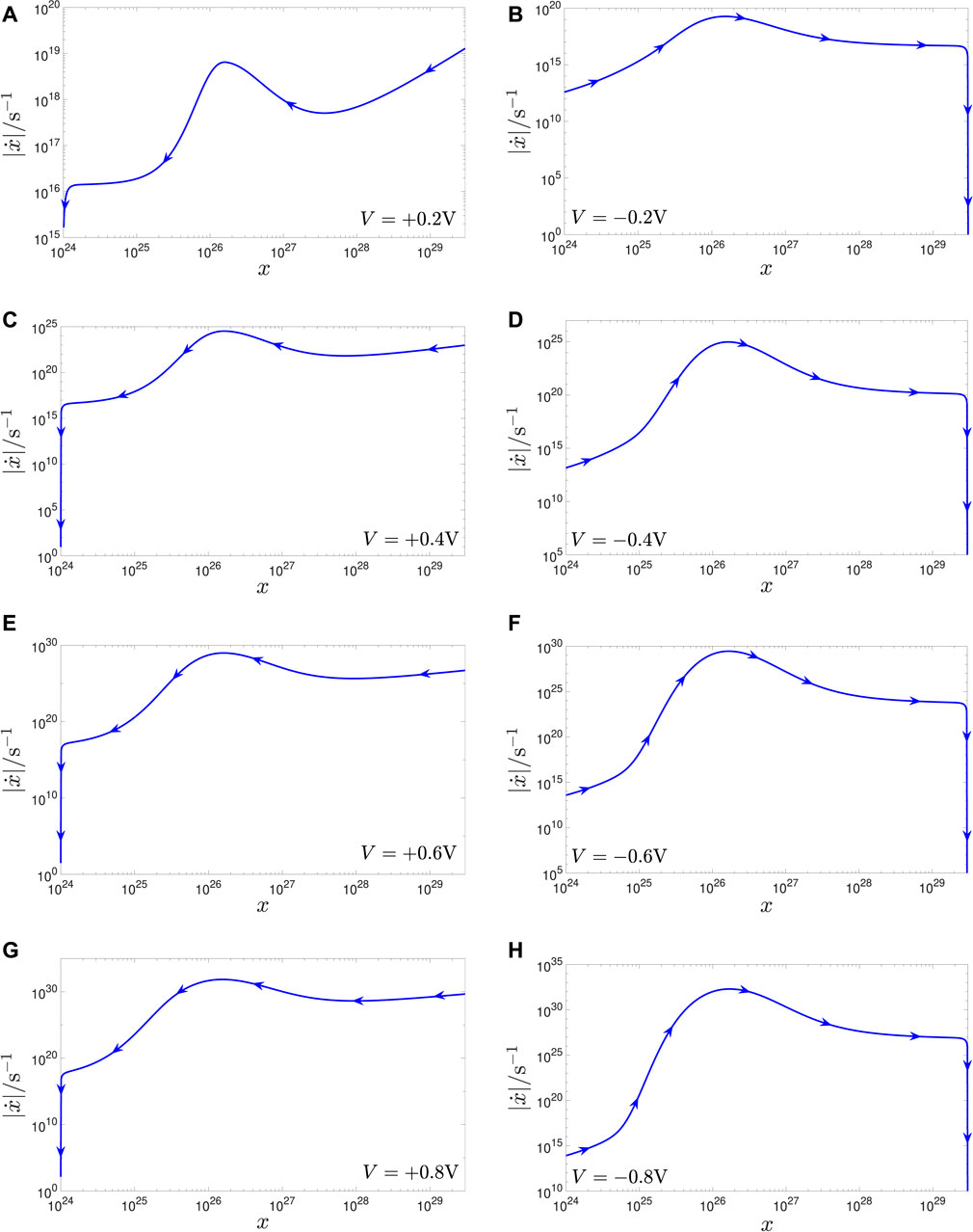
Figure 5. (A, C, E, G) ((B, D, F, H)) Family of |g (x, V)| versus x loci, for V = V+(V−) ∈ {+ (−)0.2, + (−)0.4, + (−)0.6, + (−)0.8}V, according to the predictions of the JART VCM model. The first (latter) family illustrates the multi-decade variation range for the RESET (SET) switching speed across the state existence domain for a number of positive (negative) DC inputs. Together, the RESET and SET SDRs, shown in the plots along the top and bottom rows, respectively, compose the DRM of the ReRAM cell.
4.3 A rigorous approach to induce monostability or multistability in the memristor oscillatory response to square pulse train stimulation
Equation 11, expressing the condition for a crossing between the loci of the moduli of the SET and RESET TA-SE components to appear at a given time-average state value, say at
where
stands for the ratio between the width of the positive RESET pulse and the width of the negative SET pulse, while
denotes the modulus of the ratio between two copies of the state evolution function, evaluated at a common time-average state
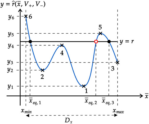
Figure 6. Representative diagram, illustrating the basics of the methodology, which is adopted in this work to study the bifurcations in the number of equilibria for the TA-SE under pulse width ratio sweep, given a preliminary selection for the remaining stimulus parameters, i.e., V+ and V−. Blue curve: locus of the function
On the basis of these insights, it is possible to propose a systematic procedure, which, given the heights V+ and V− of the RESET and SET pulses, composing the ReRAM cell stimulus over the first τ+-long and second τ−-long parts of each cycle, respectively, allows determining the number of intersections between the graph of the function
1. Calculate the ordinates of the local extrema of
2. Given the ith y-value yi from the resulting tuple (y1, y2, … yi, … , yn), with y1 < y2 < … < yi < … < yn, compute the parameter Δi, denoting the change in the number of intersections between the graph of the function
3. Focussing finally on the partition of the one-dimensional space, spanned by the parameter r, while the graphs of the functions
In the section to follow, the rigorous system-theoretic methodology, based upon the time averaging method, as presented above, shall be applied to the JART VCM model so as to demonstrate its power to predict the correspondence between the choice for the pulse width ratio of the two square pulses, composing the train voltage stimulus over each cycle, and the number of stable asymptotic oscillatory solutions for the periodically forced state equation, upon an exemplary preliminary selection for the pulses’ heights.
5 Application of the methodology
In this section, the systematic methodology, proposed in Section 4.3, is applied to an exemplary scenario14, associated with a particular choice for the pair (V+, V−), whose first (second) component specifies the height V+ (V−) of the first RESET (second SET) square pulse in the waveform of the AC periodic pulse train voltage stimulus over each cycle. For this scenario, the
5.1 Exemplary scenario
Figure 7 shows the dependence of
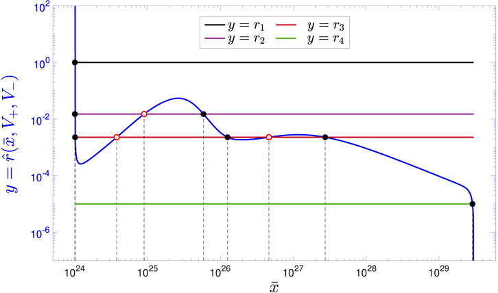
Figure 7. Blue trace: locus of
5.1.1 Case study 1.1: monostable oscillatory response around the fully-RESET state
Choosing r = r1 = 1 (refer to the horizontal black line in Figure 7), the proposed system-theoretic method predicts a unique oscillatory operating mode around the fully-RESET state for the TaOx ReRAM cell manufactured at FZJ. Assigning the common value of 10 ⋅ 103s to both τ− and τ+, the resulting periodic voltage stimulus vS, applied across the memristor, is shown in plot (a) of Figure 8. Here, the TA-SDR predicts a single globally asymptotically stable (GAS) oscillatory solution for the device memory state, as depicted in plot (b) of the same figure. As, in this case study, the only equilibrium
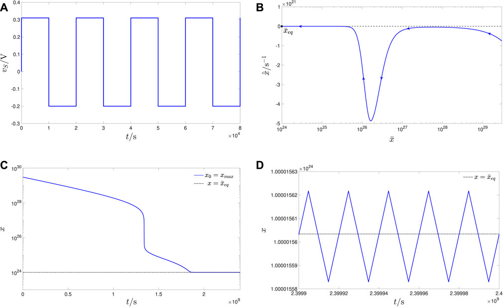
Figure 8. (A) Time waveform of the periodic voltage signal vS, which, let fall across the ReRAM cell, enforces its steady-state operation as a monostable oscillator around the fully-RESET state (case study 1.1). The first (second) positive (negative) RESET (SET) pulse in each cycle of the train features an amplitude V+ (V−) of +0.31 V (−0.2 V), as established via Figure 7, for all case studies in this section. The common value of 10 ⋅ 103 s is assigned to the RESET τ+ and SET τ− pulse widths, implying T = τ+ + τ− = 20 ⋅ 103s and r = r1 = 1. (B) TA-SDR, associated with the input from (A) and predicting a single GAS equilibrium
5.1.2 Case study 1.2: coexistence of two stable oscillatory operating modes, one of which is around the fully-RESET state
In Figure 1A, a triangular periodic voltage waveform was employed to stimulate the ReRAM cell so as to endow it with oscillatory bistability, similarly as first reported in (Ascoli et al., 2022), where, however, no theoretical analysis was provided to explain the coexistence of two periodic solutions, one of which affected by the RESET boundary condition, for the memory state. In this case study, the system-theoretic method, described in Section 3, is employed to shape a square wave voltage stimulus in such a way to induce a similar nonlinear dynamic phenomenon in the device. In particular, keeping the positive (negative) height V+ (V−) of the first (second) pulse in each cycle of the input voltage train unaltered relative to case study 1.1, this may be achieved by setting the RESET-to-SET pulse width ratio r to r2 = 1.5 ⋅ 10–2, as may be inferred by inspecting the number of crossings between the violet horizontal line and the blue curve in Figure 7, as well as the slope of the latter trace at each of their locations. Figure 9A shows a periodic voltage stimulus, satisfying these constraints, for τ+ = 1 ⋅ 104s and τ− = 6.667 ⋅ 105s. Under this periodic excitation, the TA-SE of the ReRAM cell admits three equilibria, specifically
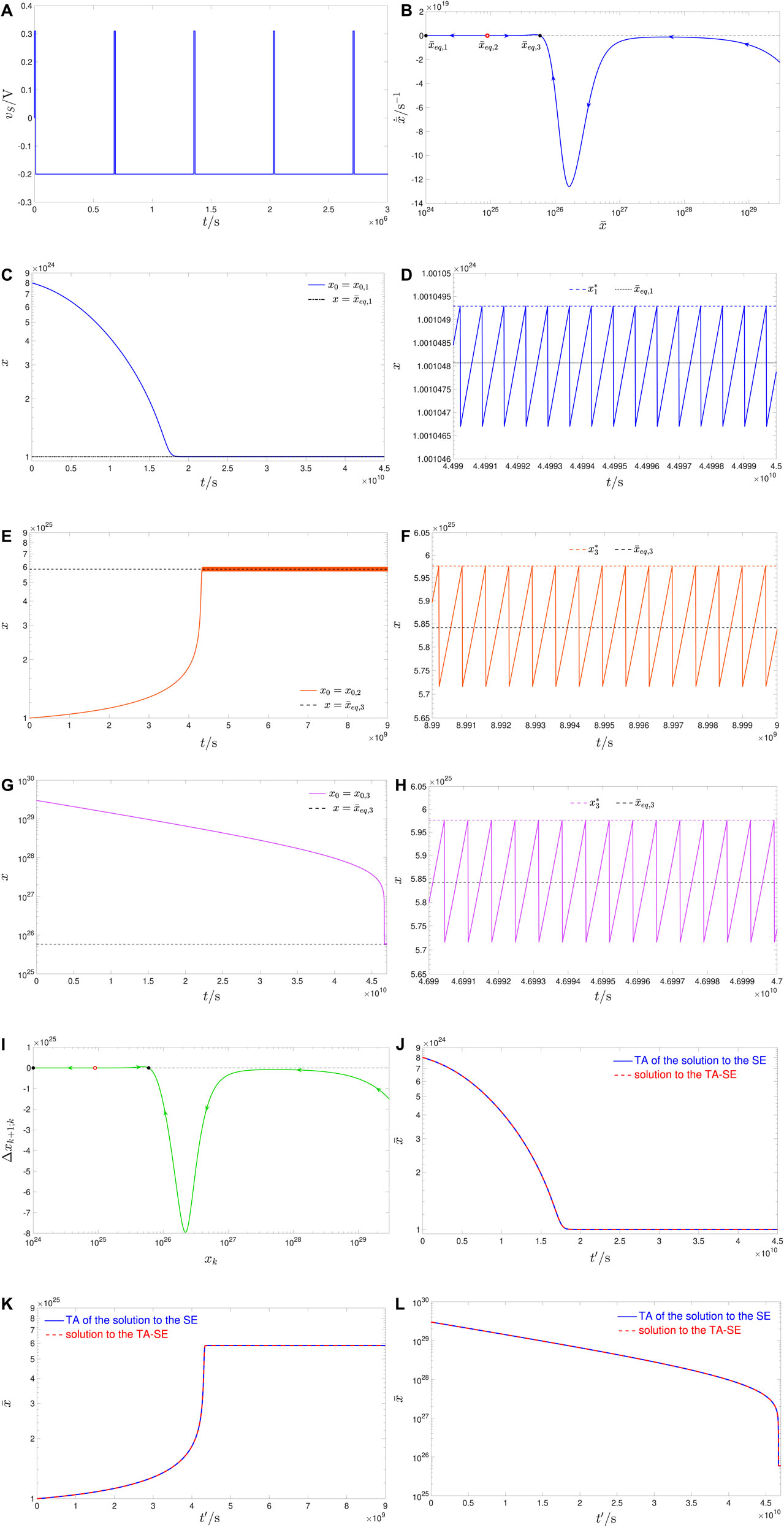
Figure 9. (A) Time course of the two-pulse-per-cycle train voltage signal, which induces a bistable oscillatory response in the ReRAM cell (case study 1.2). The RESET τ+ and SET τ− pulse width parameters, identifying unequivocally the AC periodic stimulus, together with the fixed values + 0.31 V and −0.2 V, set in turn for the RESET V+ and SET V− pulse amplitudes, in the scenario Figure 7 refers to, are taken here as 1 ⋅ 104s, and 6.667 ⋅ 105s, respectively. (B) Resulting TA-SDR for the periodically driven ReRAM cell, revealing the existence of three equilibria, specifically
Plots (c), (e), and (g) of Figure 9, respectively, show the time evolution of the memory state, as recorded from transient simulations of the DAE set (Eqs 1, 2), extracted numerically from the JART VCM model, as described in Supplementary Appendix A.1, covering a time span of 70,000, 14,000, and 70,000 cycles, respectively, and resulting upon fixing preliminarily the initial memristor state x0 to the first, second, and third values from the set S1 = {x0,1, x0,2, x0,3} = {8 ⋅ 1024, 1 ⋅ 1025, 3 ⋅ 1029}. With reference to Figure 9C, the solution of the JART VCM DAE set, starting off from the first initial condition in S1, descends progressively toward a steady-state oscillatory waveform, which is found to revolve around the leftmost locally stable TA-SE equilibrium
5.1.3 Case study 1.3: coexistence of three stable oscillatory operating modes, one of which is around the fully-RESET state
The brown horizontal line y = r3 = 2.3 ⋅ 10–3 from Figure 7 meets the locus of
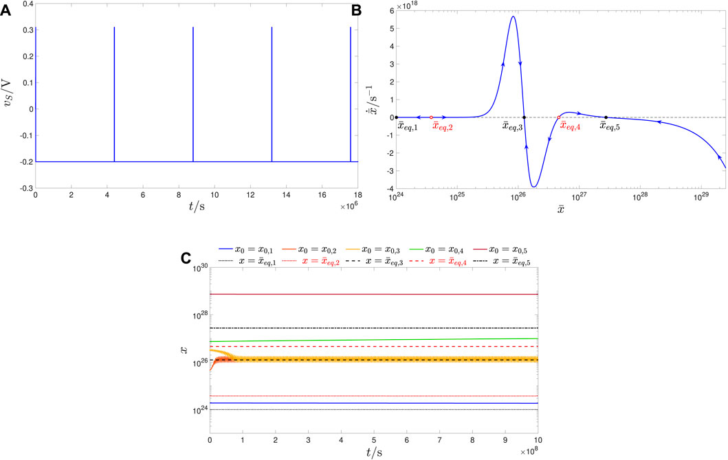
Figure 10. (A) Two-pulse-per-cycle periodic voltage signal vS, to be applied across the TaOx nanodevice so as to endow it with a tristable oscillatory behaviour (case study 1.3). The pulse height–width pair for the first (second) positive (negative) RESET (SET) pulse in each period of the stimulus is (V+, τ+) = (+0.31 V, 10 ⋅ 103s) ((V−, τ−) = (−0.2 V, 4.385 ⋅ 106s)). Here, r = r3 = 2.3 ⋅ 10–3, while T = τ+ + τ− = 4.395 ⋅ 106s. (B) TA-SDR of the ReRAM cell under the periodic excitation illustrated in (A). Five are the intersections between the TA-SDR and the horizontal axis, specifically
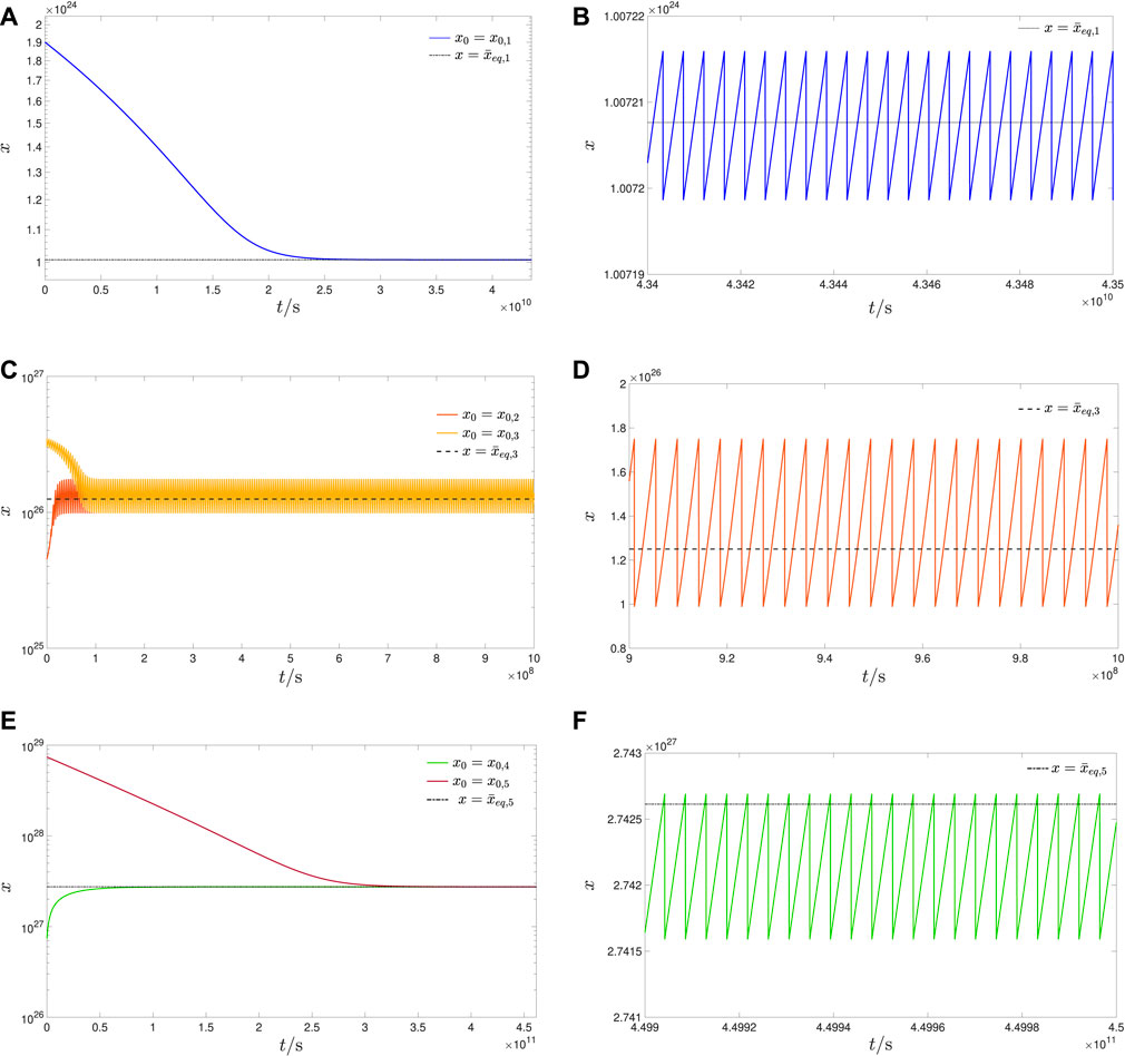
Figure 11. (A, C, E) Time waveform of the memory state x of the ReRAM cell, modelled by means of the JART VCM mathematical description (Bengel et al., 2022), as, respectively, recorded during transient simulations of the test circuit of Figure 2A over 250, 10,000, and 105,000 cycles of the AC periodic voltage stimulus, illustrated in Figure 10A, as envisaged in case study 1.3, when the first, second or third, and fourth or fifth value from the set S2 ≜ {x0,1, x0,2, x0,3, x0,4, x0,5} = {1.9 ⋅ 1024, 4.6 ⋅ 1025, 3.5 ⋅ 1026, 7.5 ⋅ 1026, 7.4 ⋅ 1028} is, in turn, assigned to the device initial condition x0. In the first, second, and third plots from this triplet, the horizontal dotted, dashed, and dash-dotted black line marks, respectively, the location of the outer left
Supplementary Appendix A.2 reports the promising results of initial investigations aimed to define an appropriate setup for a future experimental verification of tri-stability in the oscillatory device via pulse generators with physical limitations.
5.1.4 Case study 1.4: monostable oscillatory response around the fully-SET state
Setting r to r4 = 1 ⋅ 10–5 (see the green horizontal line in Figure 7), the memristor is expected to lock into a unique oscillatory operating mode around the fully-SET state. Indeed, this is the case. Keeping the positive (negative) height V+ (V−) of the first (second) RESET (SET) pulse in each cycle of the input train, as specified in all the case studies in the exemplary scenario, Figure 7 refers to, and setting its temporal width τ+ (τ−) to 102s (105s), which meets the requirement on r, results in the voltage stimulus, illustrated in Figure 12A. Here, the TA-SE (Eq. 7) admits one and only one equilibrium
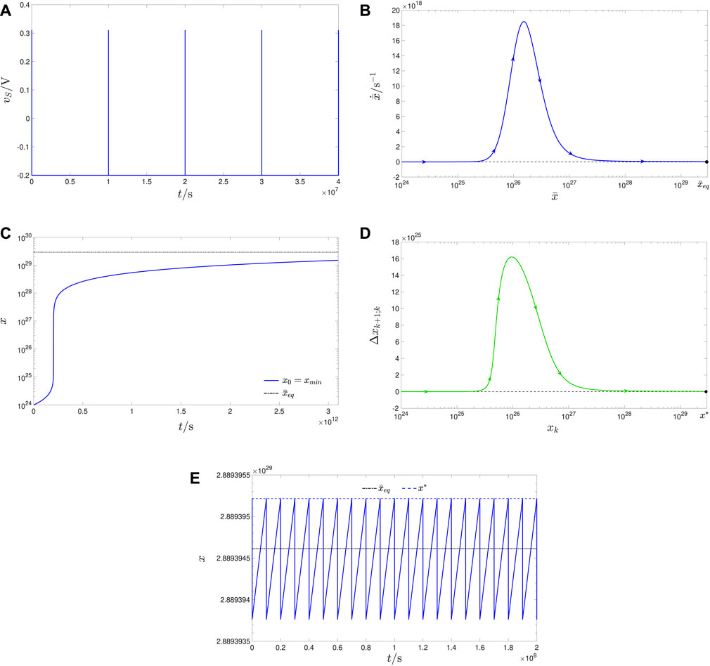
Figure 12. (A) Time course of the pulse train-based voltage stimulus vS, to be applied across the ReRAM cell, manufactured at FZJ, in order to induce monostable oscillatory dynamics around the fully-SET state across its physical medium (case study 1.4). The values for the four parameters, defining its two square pulses per cycle, are V+ = +0.31 V, τ+ = 1 ⋅ 102s, V− = −0.2 V, and τ− = 1 ⋅ 107s (T = τ+ + τ− = 1.00001 ⋅ 107s, r = r4 = 1 ⋅ 10–5). (B) TA-SDR of the TaOx memristor, under the periodic excitation illustrated in (A). The
6 Uncovering novel forms of device multimodal oscillatory dynamics via input pulse height parameter modulation
The exploration of other regions of the V+-V− input parameter plane revealed how wider the spectrum of oscillatory dynamics inducible in the ReRAM cell is upon pulse train stimulation. In fact, the choice of a certain pulse height parameter pair sets the periodically driven JART VCM DAE set on a given invariant manifold, characterised by distinctive oscillatory dynamics alternating one after the other via bifurcation phenomena upon pulse width ratio modulation. To name but one example15, this section explains how one may massage the pulse train properties so as to trigger the coexistence of four locally stable oscillatory solutions for the ReRAM cell memory state. Assigning +0.47 V (−0.34 V) to the RESET (SET) pulse height V+ (V−), the locus of the function
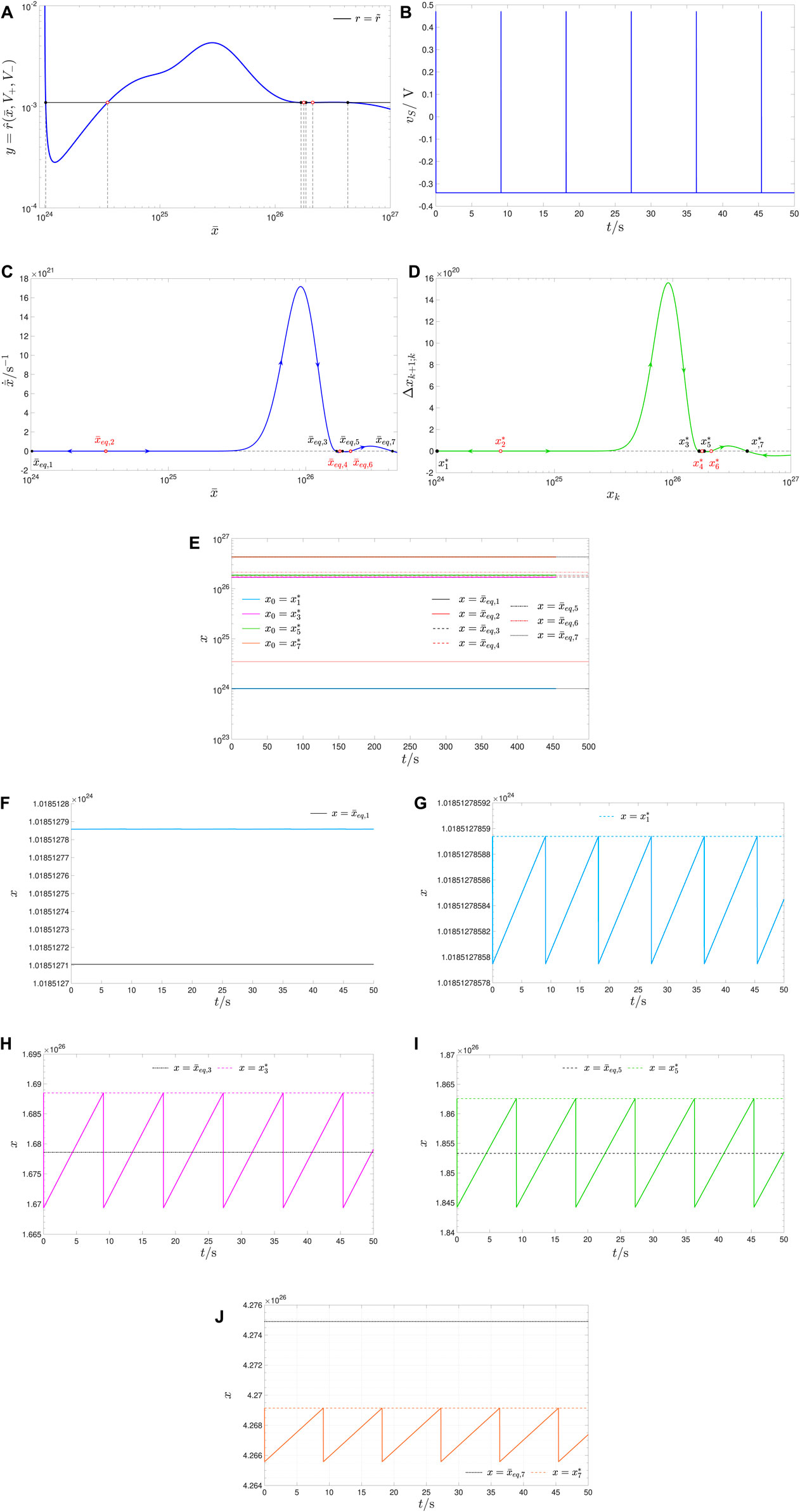
Figure 13. Coexistence of four stable oscillatory operating modes for the periodically-forced ReRAM cell under a different selection of the pulse height parameter pair and suitable pulse width ratio. (A) Blue trace: locus of
Remark 2. In view of a future experimental validation of the theory, toward a potential exploitation of the multistable oscillatory response of the periodically driven nano-device for electronics applications, the intrinsic physical limitations in the laboratory instrumentation tools should be considered. The minimum allowable rise/fall time for a square pulse, emitted by any of the AC periodic voltage sources, employable in our laboratories for generating a two-pulse-per cycle train voltage stimulus, is mandatorily 10–4 times the maximum between the widths of the SET and RESET pulses in the input waveform over each cycle. Since the narrower pulse width need to be at least one order of magnitude larger than the minimum allowable pulse rise/fall time, this directly sets a soft constraint on the upper bound for the pulse width ratio, which is allowed to range approximately within the limited value set, expressed here:
Initial investigations, aimed to craft ReRAM cell stimuli, which roughly comply with the restrictive condition (Eq. 16), have already delivered promising results, as revealed in Supplementary Appendix A.2, as well as in Section 6.
The study, described in this section, was a source of inspiration for setting up an ad hoc experiment, enabling to record the bistable oscillatory behaviour of the VCM device under suitable periodic pulse train stimulation in the laboratory, as reported, for the first time ever in the literature, in the remainder of the main text of our manuscript.
7 Experimental evidence for bistability
7.1 Device stack
The TaOx valence change memory (VCM) device, subject to the experimental test for bistability, was fabricated at the facilities of Forschungszentrum Jülich (FZJ). As shown in either plot of Figure 14, the ReRAM cell consists of a metal–insulator–metal (MIM) physical stack, where a 7-nm-thick tantalum oxide (TaOx) layer is sandwiched between a 30-nm-thick Pt layer, playing the role of the top active electrode, and sitting on top of a 430-nm-thick SiO2 substrate, and a 13-nm-thick tantalum (Ta) layer, acting as the bottom ohmic electrode, and covered by yet another 25-nm-thick Pt capping layer. Plot (a) of Figure 14 shows how voltage stimuli were applied across the device in the laboratory measurements. In the experiments, the active electrode was grounded, while the ohmic electrode was connected to the voltage source vS. Since, as illustrated in plot (b) of the same figure, the theoretical analysis, reported throughout the manuscript, assumes the application of the voltage stimulus VS to the active electrode, with the ohmic electrode grounded, in the experimental tests, the device undergoes a SET (RESET) resistance switching transition as a positive (negative) voltage vS is set to fall between its terminals. A scanning electron microscope (SEM) top-view and a transmission electron microscope (TEM) cross-sectional image of a single Pt/TaOx/Ta/Pt VCM device, occupying a junction area of 3 × 3 μm2 within a passive crossbar array, are, respectively, shown in plots (a) and (b) of Figure 15 (Ascoli et al., 2022).
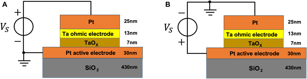
Figure 14. (A) Qualitative sketch of the device physical stack, illustrating how a voltage stimulus vS was applied between its terminals for the bistability test in the laboratory. (B) Illustration of the assumption, made for the theoretical analysis presented in the paper, on the way a voltage source vS is connected across the ReRAM cell for inducing nonlinear phenomena across its physical medium (see also Supplementary Figure 20).
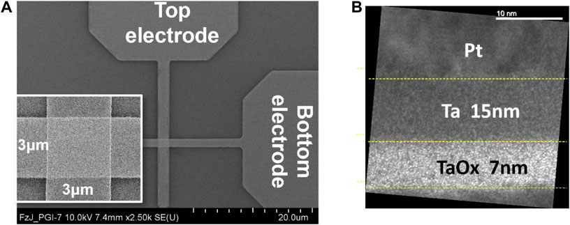
Figure 15. (A) Top-view SEM image of a VCM crosspoint device of the junction area 3 × 3 μm2. (B) Cross-sectional TEM image of a ReRAM cell of this kind, revealing the thickness of each layer in its physical stack (Ascoli et al., 2022).
7.2 Information about the measurement procedure
The setup for the measurement employs a Keithley 4200-SCS parameter analyser, outfitted with ultra-fast pulse measurement units from the 4225-PMU family, as well as with remote preamplifier/switch modules, facilitating the detection of small currents. Figure 16 showcases a photograph of the Cascade Microtech MPS150 probe station, employing a Motic PSM-1000 microscope, and a pair of manually operated DPP220 probe positioners. The Keithley 4200-SCS parameter analyser can generate periodic square-wave voltage signals with amplitudes within the range (−40 V, +40 V), widths reducible down to 70 ns, and rising, as well as falling flanks stretching across a minimum time span of 20 ns each. The same tool allows measuring currents ranging between 100 nA and 200 mA. The operation of the device is orchestrated through a custom Python script, which allows transmitting commands to the experimental apparatus and retrieving measurement data from the sample under test via a general purpose interface bus (GPIB).
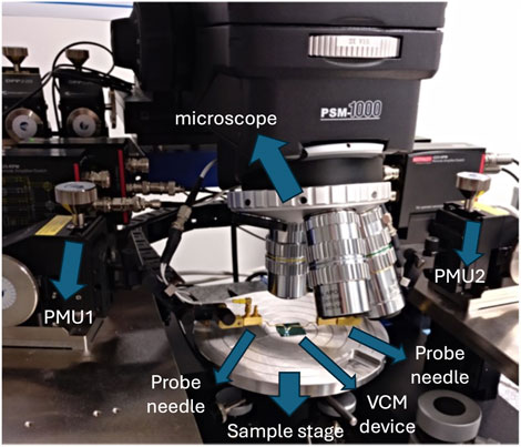
Figure 16. Probe station, including microscope, sample stage, and probe needles. Two pulse measurement units (PMUs), indicated here as PMU1 and PMU2, are also visible in the background.
To program a specific resistance state into the TaOx VCM device across the range (10 kΩ, 55 kΩ) ahead of the bistability test, an asymmetric triangular voltage stimulus vS at frequency 1 kHz, with a fixed positive SET amplitude
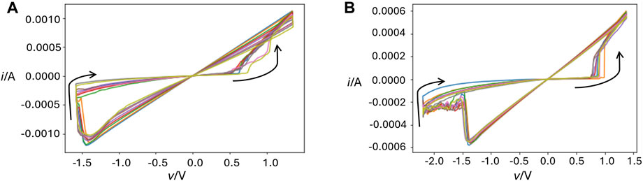
Figure 17. Current i versus voltage v loci of the ReRAM device as an asymmetric triangular voltage signal vS at frequency 1 kHz is let to fall between its terminals for 10 consecutive input cycles. The amplitude
Here, a four-pulse-per-cycle train voltage signal vS was let to fall across the device for as many as 200 cycles. In each period, the voltage source was regulated in such a way to generate, first, a negative write pulse of amplitude V− = −1.1 V and width τ− = 0.5 ms; then, after a pause of 0.01 ms, a first read pulse, featuring amplitude 0.1 V, width 1 ms, and 0.1-ms-long rising and falling flanks; subsequently, after another pause of 0.01 ms, a positive write pulse of amplitude V+ = +0.7 V and width τ+ = 0.5 ms; and finally, after yet another pause of 0.01 ms, a second read of pulse, featuring amplitude 0.1 V, width 1 ms, and 0.1-ms-long rising and falling flanks.
Importantly, as recently reported (Wiefels et al., 2023), a stochastic relaxation phenomenon emerges in the nanodevice under zero input. In particular, ions hop randomly across the powered-off physical stack at ambient temperature. These stochastic effects may result in significant changes in the device resistance over time. In fact, they explain why, for each of a few scenarios from the set of cardinality 9 under consideration, extracting 20 samples of the device current at regular time intervals as the read pulse, directly following the RESET write pulse in the first cycle of the pulse train voltage stimulus, was let to fall across the physical stack, the average resistance of the ReRAM cell was found to be lower than the respective initial condition. This happened for those scenarios indexed through the labels listed in the set {3,4,6,7,8,9}. In fact, with reference to the scenario labelled via the index i, which ranges across the set {1, 2, 3, 4, 5, 6, 7, 8, 9}, right previous to the application of the SET write pulse between its terminals in the first cycle of the pulse train voltage stimulus, the VCM device was found to admit the ith resistance in the set S2,R ≜ {R0,1, R0,2, R0,3, R0,4, R0,5, R0,6, R0,7, R0,8, R0,9} = {11.133, 14.623, 15.337, 24.586, 32.920, 26.399, 21.584, 36.571, 32.563}kΩ. For this reason, we discarded the first cycle in the train voltage stimulus vS, employed in the bistability test, using, however, its second read pulse to define a new initial condition for the VCM device as the average between 20 regularly spaced out measurements. Hence, in the ith scenario, with i ∈ {1, 2, 3, 4, 5, 6, 7, 8, 9}, directly before the application of the second sequence of four pulses across its physical stack, the ReRAM cell was found to hold the ith resistance in the set S3,R ≜ {R0,1, R0,2, R0,3, R0,4, R0,5, R0,6, R0,7, R0,8, R0,9} = {3.032, 3.456, 4.005, 4.367, 6.459, 5.243, 4.456, 30.861, 37.185}kΩ. Figure 18A shows the initial periods of the time course of the train voltage stimulus except for its first four pulses. The pulse train voltage signal induces the simplest form of local fading memory in the nanodevice, namely, a bistable oscillatory response. In fact, as shown in Figure 18B, under the application of such a periodic excitation for as many as 199 cycles, the device resistance, measured at regular time intervals, 20 times per read pulse, after each write operation over each period, was found to evolve toward one of two possible steady-state oscillatory solutions, depending upon its initial condition. In particular, the traces, associated with the 1st, 2nd, and 3rd and 4th (5th, 6th, 7th, 8th, and 9th) initial conditions from the set S3,R, progressively approach the lower (upper) oscillatory solution. It follows that the sets of initial conditions, from which the memristive system respectively asymptotically approaches the lower or the upper oscillatory attractor from the admissible pair, are separated by an initial condition lying between R0,4 = 4.367 kΩ and R0,7 = 4.456 kΩ. For resistance initial conditions above the separatrix, the device experiences much slower dynamics than otherwise. In fact, despite, as shown through red and purple traces in plot (f) of Figure 19, the experiment was iterated for as many as six iterations for two particular resistance initial conditions from S3,R, specifically R0,1 = 3.032 kΩ and R0,9 = 37.185 kΩ, falling, respectively, in the basin of attraction of the lower and upper oscillatory attractors for the periodically driven memristive system, the application of the four-pulse-per-cycle train voltage stimulus across the physical stack for as many as 1,200 periods was insufficient for transients to vanish for the initial condition above the separatrix, which prevented the observation of the upper steady-state oscillation in the device resistance at the end of the experiment. This notwithstanding, it is the pure existence of the separatrix (Strogatz, 2014), which provides firm evidence for the bistability of the periodically forced ReRAM cell.
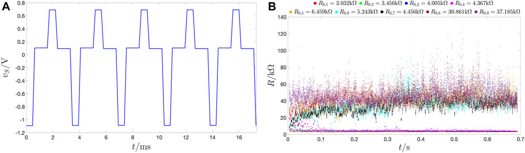
Figure 18. (A) Time course of the four-pulse-per-cycle train voltage stimulus vS, let to fall across a VCM device sample in the laboratory, as measured over the first five periods. (B) Transient evolution of the device resistance, sampled at 20 regularly spaced time instants after each RESET or SET writes pulse, toward a lower (an upper) locally stable steady-state oscillatory solution from any of the first four (last five) initial conditions from the set S3,R ≜ {R0,1, R0,2, R0,3, R0,4, R0,5, R0,6, R0,7, R0,8, R0,9} = {3.032, 3.456, 4.005, 4.367, 6.459, 5.243, 4.456, 30.861, 37.185}kΩ, as recorded from the 2nd to the 200th input period. As a result, the initial condition, separating the basins of attraction of the two admissible locally stable oscillatory solutions for the resistance R at steady state, lies between R0,4 = 4.367 kΩ and R0,7 = 4.456 kΩ.
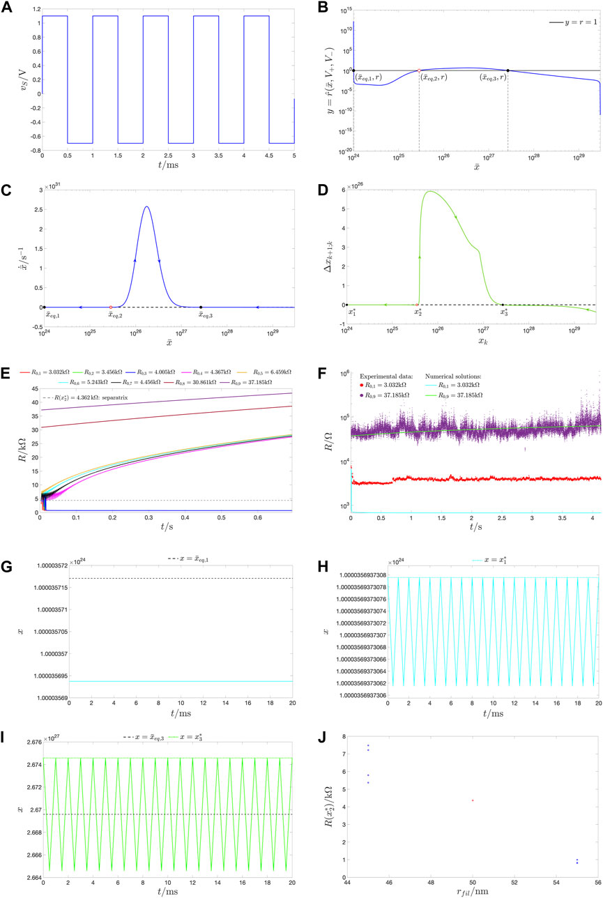
Figure 19. (A) Time waveform of a two-pulse-per-cycle train voltage stimulus vS, used as the memristor voltage v in the numerical simulation of the JART VCM v1 model for reproducing qualitatively the experimental observations, across the first five periods. The amplitude V+ (V−) of the first (second) RESET (SET) pulse in each cycle is chosen as 1.1 V (−0.7 V). The RESET and SET pulse widths, respectively, referred to as τ+ and τ−, are assumed to be identical and set to 0.5 ms each. (B) Graph of
Since the device sample, employed in the experimental test for bistability, is different from the one, the JART VCM model, used for the system-theoretic analysis reported so far in this paper, was originally (Ascoli et al., 2022) fitted to, a parameter tuning procedure had to be run once again to match qualitatively the behaviour of its solutions to the measurement data from Figures 18B, 19F. A standard optimisation algorithm, massaging a few parameters, specifically e ⋅ ϕbn0, Rth,eff,RESET, and Rth,eff,SET, in such a way to minimise the error between the model predictions and these experimental measurements, resulted in their update, relative to the nominal values in Supplementary Table A1, as listed at the end of Supplementary Appendix A.1 (refer to Supplementary Table A2). In order to simplify the numerical integration of the JART VCM model, the read pulses were omitted from the voltage signal assumed to fall across the memristor. In fact, as shown in Figure 19A, in the numerical simulation, replicating qualitatively the experimental data, vS was shaped as a two-pulse-per-cycle train voltage stimulus. Taking into account the different approach, employed in the model simulation to apply the voltage stimulus across the ReRAM cell (recall Figure 14B), as compared to what was performed in the experiment (recall Figure 14A), the first (second) pulse within each T = 1-ms-long period of the input signal vS is assumed to undergo a RESET (SET) transition in the nanodevice, featuring an amplitude V+ of +1.1 V (V− of −0.7 V) and a width τ+ of 0.5 ms (τ− of 0.5 ms). Figure 19B shows the
Interestingly, the device resistances, computed at the read voltage level V of −0.1 V at the first, second, and third TA-SE equilibria, respectively, read as
Figure 19E shows the model prediction for the time course of the device resistance from each of the initial conditions, falling in the set
The separatrix point, appearing at
8 Conclusion
Typically, the application of a periodic stimulus, from classes commonly used in electrical engineering, including sine-waves, triangular waves, and square waves, to a non-volatile resistance switching memory induces a unique, i.e., initial condition-independent asymptotic oscillatory response in its memory state (Ascoli et al., 2017), a property referred to as fading memory (Boyd and Chua, 1985). On the other hand, local fading memory effects are said to emerge in a system, which, under the effects of some input, may asymptotically exhibit a number of different behaviours, locking into each of the possible operating modes for all initial conditions from the respective basin of attraction (Ascoli et al., 2016a; Ascoli et al., 2016b). A numerical investigation (Ascoli et al., 2022), based upon a predictive model (Hardtdegen et al., 2018; Bengel et al., 2022), recently unveiled the emergence of bistability, i.e., the simplest form of local fading memory, in the oscillatory response of the physical realization of a tantalum oxide ReRAM cell to a particular periodic triangular stimulus. However, the manuscript, reporting this interesting observation, made independently also from other scientists, exploring the non-linear dynamics of a different non-volatile memristor via bifurcation analysis (Pershin and Slipko, 2019), provided no further analysis to elucidate the origin for the coexistence of two stable oscillatory steady states for the nano-device. As another open question, stemming from this research work, it would be of interest to understand how to modulate the properties of the stimulus so as to induce the emergence of bifurcation phenomena, whereby the nature of the fading memory effects, appearing in the device, would switch from local to global or vice versa. Investigating whether there exist periodic excitations, inducing more complex forms of local fading memory than bistability in the nano-device, is a follow-up problem worthy of study. A theoretical research work is first presented in this manuscript to provide comprehensive answers to all these questions. In particular, the state dynamic route technique, inspired to the time averaging methodology (Guckenheimer and Holmes, 1983) from the theory of non-linear dynamics, and to the bifurcation study, reported in Pershin and Slipko (2019), is first introduced as extension of the dynamic route map graphic tool (Chua, 2018), which is applicable to the analysis of first-order systems subject to bias inputs only, for the exploration of the response of systems of this kind to AC periodic square pulse train-based stimuli. Recurring to this technique, a rigorous and systematic strategy is then set up to massage heights and widths of the two square pulses of opposite polarity, composing a periodic pulse train-based input over each cycle, so as to modulate the number and stability properties of the admissible oscillatory steady states of the nano-device. Numerical simulations of the device model in a number of excitation scenarios provide robust proof of evidence for the accuracy of the proposed theoretical framework in predicting all the possible levels, around which the state of the memristor, subject to a periodic two-pulse-per-cycle train stimulus, may be found to revolve, after transients vanish, for a given choice of the four input parameters. Toward the experimental verification of the theory, developed in this research study, the intrinsic physical limitations to the measurement instrumentation tools need to be taken into account for the definition of an ad hoc input parameter setting in each case study. In this regard, as shown in Section 6, margins for experimental setup optimization exist, given that the set of bifurcations in number, stability, and kinds of oscillatory solutions for the memory state of the ReRAM cell upon a pulse width ratio sweep varies critically with the pulse height parameter pair selection, which widens considerably the spectrum of opportunities available to the circuit designer17. On the basis of these considerations, as reported in Section 7, we were able to devise an opportune experimental setup, through which we confirmed the theoretical predictions on the bistable oscillatory response of the ReRAM cell under suitable periodic pulse train stimulation in the laboratory, as reported at the end of the manuscript. In particular, the experimental analysis, corroborating the accuracy of our theory, allowed identifying the signature for the bistability of the periodically forced nanodevice, namely, the existence of an initial condition for its resistance, separating the basins of attraction of its two admissible oscillatory steady states. To the best of our knowledge, this is the first time local fading memory effects, resulting in steady-state bistability, are discovered at the nanoscale in a non-volatile resistance switching memory! Importantly, numerical investigations of the JART VCM model further showed how a separatrix point keeps existing across the allowable domain for the ReRAM cell resistance even under non-negligible device-to-device variability effects. Moreover, as described in Supplementary Appendix A.2, the application of the system-theoretic framework, presented in this paper, under the additional constraint, allowing the SET and RESET pulse widths to differ by three orders of magnitude at most, enables determining an appropriate input parameter quartet for the execution of a practical tristability test on the oscillatory device in the laboratory. The theoretical prediction of the coexistence of more than two oscillatory steady states in the nanodevice for suitable periodic excitations awaits now for experimental verification. Moreover, toward a future exploitation of these peculiar nonlinear phenomena for electronics applications, one of the tasks to fulfil involves the inclusion of non-idealities, especially those factors responsible for stochastic cycle-to-cycle electrical behavioural variability, in the ReRAM cell model to understand how they affect the shape of the
Data availability statement
The raw data supporting the conclusion of this article will be made available by the authors, without undue reservation.
Author contributions
NS: conceptualization, data curation, formal analysis, investigation, methodology, validation, and writing–review and editing. AA: conceptualization, data curation, formal analysis, investigation, methodology, supervision, validation, visualization, writing–original draft, and writing–review and editing. IM: investigation and writing–review and editing. ASD: investigation and writing–review and editing. SM: investigation and writing–review and editing. VR: investigation and writing–review and editing. RT: formal analysis, validation, and writing–review and editing. LC: formal analysis, validation, and writing–review and editing.
Funding
The author(s) declare that financial support was received for the research, authorship, and/or publication of this article. LC is supported in part by the United States Air Force Office of Scientific Research (AFOSR) grant number FA 9550-18-1-0016. The Deutsche Forschungsgemeinschaft is also acknowledged for the financial support to the project “Universal Memcomputing in Hardware Realizations of Memristor Cellular Nonlinear Networks” (project number: 441957207).
Acknowledgments
The authors are thankful to Sitandi Zhang (Forschungszentrum Jülich) for performing the experiments, discussed in Section 7, which allowed validating the theory developed in this scientific study. They are also grateful to Prof. Marco Gilli (Politecnico di Torino) and Prof. Fernando Corinto (Politecnico di Torino) for their precious contributions in the theoretical analysis of the bistability of the periodically forced ReRAM cell from Forschungszentrum Jülich over the entire course of this research work. They also extend their gratitude to Vasilis Ntinas (Technische Universität Dresden) and Dimitris Prousalis (Technische Universität Dresden) for contributing to the numerical investigations, allowing to refit the JART VCM v1 model to the experimental data and to verify the robustness of the bistability of the device against its intrinsic cycle-to-cycle variability. Last but not least, Tim Kempen (Forschungszentrum Jülich) is sincerely acknowledged for the provision of insightful recommendations for the numerical investigations, reported in Supplementary Appendix A.2, devoted to the identification of a suitable parameter setting for a periodic square wave voltage stimulus, allowing, as next step of our research, the pursuit of an experimental tristability test on the oscillatory ReRAM cell, taking into account the physical limitation of the pulse generators available at our laboratories.
Conflict of interest
The authors declare that the research was conducted in the absence of any commercial or financial relationships that could be construed as a potential conflict of interest.
The handling editor CR declared a past co-authorship with the author AA.
Publisher’s note
All claims expressed in this article are solely those of the authors and do not necessarily represent those of their affiliated organizations, or those of the publisher, the editors, and the reviewers. Any product that may be evaluated in this article, or claim that may be made by its manufacturer, is not guaranteed or endorsed by the publisher.
Supplementary material
The Supplementary Material for this article can be found online at: https://www.frontiersin.org/articles/10.3389/fnano.2024.1301320/full#supplementary-material
Footnotes
1Applying a positive (negative) voltage stimulus at the Pt electrode, while grounding the Ta electrode, a RESET (SET) resistance switching transition is induced in the Ta/TaOx/Pt device stack manufactured in Jülich.
2An ODE is said to be non-autonomous if it is forced by a non-constant input. Else, it is an autonomous system.
3Importantly, the Poincaré map technique allows studying a periodically forced continuous-time system, which is equivalent to a second-order autonomous ODE, in which the time variable encodes one degree of freedom, through a simpler one-dimensional discrete-time system.
4Note that, inverting the order of the RESET and SET pulses in the periodic voltage stimulus vS, depicted in Figure 1A, the two stable fixed points for the new map, which would be extracted in this other excitation scenario, would correspond to the minima for two locally stable steady-state oscillations in the memory state.
5Despite its high predictive accuracy, the SCPCM technique (Ascoli et al., 2023b) relies on numerical integrations, and, for this reason, is not employable to resolve this open question. It may be used, however, to verify the predictions from the time-averaging method, which holds validity only in periodic excitation scenarios, which induce small changes in the state per cycle Ascoli et al. (2022).
6For the sake of simplicity,
7As anticipated in Section 2, when a positive (negative) voltage v is let to fall between the Ta and Pt electrodes of the device stack from Jülich, the device undergoes a RESET (SET) transition. Moreover, as the state evolution function g(x, v) in the JART model is anti-sign invariant (Chua, 2018), implying g(x, v) < (>)0 for v > (<)0, the state variable decreases (increases) in a RESET (SET) transition. In fact, in such a model, x = xmin (x = xmax) corresponds to the fully-RESET (fully-SET) state for the device.
8The right hand side of Eq. 7 may be referred to as the time-average state evolution function.
9Referring, without loss of generality, to an anti-sign invariant state evolution function, the locus of the right hand side of the SE (Eq. 1) versus the memory state for a given positive (negative) DC voltage v = V = V+(V−) is referred to as a RESET (SET) state dynamic route, RESET SDR (SET SDR) for short. The families of RESET and SET SDRs compose the DRM of the first-order memristor.
10Numerical investigations, based upon the JART VCM model, already revealed (Ascoli et al., 2022) that the level, around which the memory state x of the TaOx ReRAM cell, manufactured at FZJ, is found to oscillate, after transients vanish, for a given initial condition x0, under the effect of a purely-AC periodic triangular voltage stimulus vS of suitable amplitude
11At a local extremum, the derivative of the function
12The regions (0, y1) and (y6, ∞) of the one-dimensional parameter space are uninteresting from a practical viewpoint as they correspond to unaccessible values for the memristor state.
13An exhaustive numerical exploration of the V+–V− input parameter plane allows to choose RESET and SET input pulse heights so as to obtain a desired shape for the
14V+ (V−) is intentionally chosen as the amplitude of the positive RESET (negative SET) pulse in each cycle of the asymmetric periodic triangular voltage stimulus adopted to excite the ReRAM cell in the simulation illustrated in Figure 1.
15As a further example, by appropriate choice for the input parameters, it is also possible to endow the memristor with one and only one oscillatory operating mode, envisaging a swing for its resistance well-confined within the allowable range. As the main focus of this research paper is to explore multistability in the oscillatory response of the periodically pulse-driven ReRAM cell, the analysis of a case study of this kind is omitted from the investigations.
16Plot (f) in Figure 13 shows the TA-SDR prediction
17It is worth pinpointing that the rich oscillatory dynamics, reported in this manuscript, was induced in the ReRAM cell via a simple square wave stimulus, including just two pulses per cycle. Adding more pulses within the input period is expected to increase the complexity of the dynamical phenomena emerging consequently across the device physical medium.
References
Ascoli, A., Menzel, S., Rana, V., Kempen, T., Messaris, I., Demirkol, A. S., et al. (2022). A deep study of resistance switching phenomena in TaOx ReRAM cells: system-theoretic dynamic Route map analysis and experimental verification. Adv. Electron. Mater. 8 (8), 2200182. doi:10.1002/aelm.202200182
Ascoli, A., Schmitt, N., Messaris, I., Demirkol, A. S., Strachan, J. P., Tetzlaff, R., et al. (2024). An analytical approach to engineer multistability in the oscillatory response of a pulse-driven ReRAM. Sci. Rep. 14 (5626), 5626. doi:10.1038/s41598-024-55255-7
Ascoli, A., Schmitt, N., Messaris, I., Demirkol, A. S., Tetzlaff, R., and Chua, L. O. (2023b). The State Change Per Cycle Map: a novel system-theoretic analysis tool for periodically driven ReRAM cells. Front. Electron. Mater. 23, 32. doi:10.3389/femat.2023.1228899
Ascoli, A., Schmitt, N., Messaris, I., Demirkol, A. S., Tetzlaff, R., Strachan, J. P., et al. (2023a). “Local fading memory effects in a tantalum oxide ReRAM cell from Hewlett packard labs,” in Proceedings of the IEEE Int. Conference on Metrology for Extended Reality, Artificial Intelligence and Neural Engineering (MetroXRAINE), Milano, Italy, October 25-27, 2023 (IEEE).
Ascoli, A., Tetzlaff, R., and Chua, L. O. (2016a). The first ever real bistable memristors–Part I: theoretical insights on local fading memory. IEEE Trans. Circuits Systems–II Express Briefs 63 (12), 1091–1095. doi:10.1109/tcsii.2016.2604567
Ascoli, A., Tetzlaff, R., and Chua, L. O. (2016b). The first ever real bistable memristors–Part II: design and analysis of a local fading memory system. IEEE Trans. Circuits Systems–II Express Briefs 63 (12), 1096–1100. doi:10.1109/tcsii.2016.2613560
Ascoli, A., Tetzlaff, R., Chua, L. O., Strachan, J. P., and Williams, R. S. (2016c). History erase effect in a non-volatile memristor. IEEE Trans. Circuits Systems–I (TCAS–I) Regul. Pap. 63 (3), 389–400. doi:10.1109/tcsi.2016.2525043
Ascoli, A., Tetzlaff, R., Chua, L. O., Strachan, J. P., and Williams, R. S. (2017). “Memory loss in a tantalum oxide memristor,” in Pages 94–101 of: Advances in Science and Technology, Proc. Int. Conference on Smart Materials, Structures and Systems (Perugia, Italy, 5-9 June 2016), vol. 99, Perugia, Italy, 5-9 June 2016 (Switzerland: Trans Tech Publications).
Ascoli, A., Tetzlaff, R., and Menzel, S. (2018). Exploring the dynamics of real-world memristors on the basis of circuit theoretic model predictions. IEEE Circuits Syst. Mag. 18 (2), 48–76. doi:10.1109/mcas.2018.2821760
Bengel, C., Siemon, A., Cüppers, F., Hoffmann-Eifert, S., Hardtdegen, A., von Witzleben, M., et al. (2020). Variability-aware modeling of filamentary oxide-based bipolar resistive switching cells using SPICE level compact models. IEEE Trans. Circuits Systems–I Regul. Pap. 67 (12), 4618–4630. doi:10.1109/tcsi.2020.3018502
Bengel, C., Zhang, D. K., Waser, R., and Menzel, S. (2022). JART VCM v1 verilog-A compact model user guide. Available at: https://www.emrl.de/JART-files/User_Guide_for_the_JART_VCM_v1_Compact_Model.pdf.
Boyd, S., and Chua, L. O. (1985). Fading memory and the problem of approximating nonlinear operators with Volterra series. IEEE Trans. Circuits Syst. 32 (11), 1150–1161. doi:10.1109/tcs.1985.1085649
Buckwell, M., Ng, W. H., Mannion, D. J., Cox, H. R. J., Hudziak, S., Mehonic, A., et al. (2021). Neuromorphic dynamics at the nanoscale in silicon suboxide RRAM. Front. Nanotechnol. 3 (699037), 10. doi:10.3389/fnano.2021.699037
Chua, L. O. (2018). Five non-volatile memristor enigmas solved. Appl. Phys. A 124 (563), 563. doi:10.1007/s00339-018-1971-0
Corinto, F., Civalleri, P. P., and Chua, L. O. (2015). A theoretical approach to memristor devices. IEEE J. Emerg. Sel. Top. Circuits Syst. (JETCAS) 5 (2), 123–132. doi:10.1109/jetcas.2015.2426494
Corinto, F., Forti, M., and Chua, L. (2021) Nonlinear circuits and systems with memristors: nonlinear dynamics and analogue computing via the flux-charge analysis method. 1. Cham: Springer.
Di Ventra, M., and Traversa, F. L. (2018). Perspective: memcomputing: Leveraging memory and physics to compute efficiently. J. Appl. Phys. 123 (180901), 15. doi:10.1063/1.5026506
Goswami, S., Pramanick, R., Patra, A., Rath, S. P., Foltin, M., Ariando, A., et al. (2021). Decision trees within a molecular memristor. Nature 597 (7874), 51–56. doi:10.1038/s41586-021-03748-0
Guckenheimer, J., and Holmes, P. (1983) Nonlinear oscillations, dynamical systems, and bifurcations of vector fields. 1. New York, USA: Springer-Verlag New York, Inc.
Hardtdegen, A., La Torre, C., Cüppers, F., Menzel, S., Waser, R., and Hoffmann-Eifert, S. (2018). Improved switching stability and the effect of an internal series resistor in HfO2/TiOx bilayer ReRAM cells. IEEE Trans. Electron Devices 65 (8), 3229–3236. doi:10.1109/ted.2018.2849872
Hu, M., Strachan, J. P., Li, Z., Grafals, E. M., Davila, N., Graves, C., et al. (2016). “Dot-product engine for neuromorphic computing: programming 1T1M crossbar to accelerate matrix-vector multiplication,” in Proceedings of the Design Automation Conference (DAC), Austin Texas, June 5 - 9, 2016.
Ielmini, D., and Waser, R. (2016) Resistive switching: from fundamentals of nanoionic redox processes to memristive device applications. 1. Wiley-VCH Verlag GmbH & Co. KGaA.
La Torre, C., Zurhelle, A. F., and Menzel, S. (2019). “Compact modelling of resistive switching devices based on the valence change mechanism,” in Proc. of the Int. Conf. on Simulation of Semiconductor Processes and Devices (SISPAD), Udine, Italy, 4-6 September 2019.
Lenk, C., Hövel, P., Ved, K., Durstewitz, S., Meurer, T., Fritsch, T., et al. (2023). Neuromorphic acoustic sensing using an adaptive microelectromechanical cochlea with integrated feedback. Nat. Electron. 6, 370–380. doi:10.1038/s41928-023-00957-5
Li, C., Hu, M., Li, Y., Jiang, H., Ge, N., Montgomery, E., et al. (2018). Analogue signal and image processing with large memristor crossbars. Nat. Electron. 1 (1), 52–59. doi:10.1038/s41928-017-0002-z
Marchewka, A., Roesgen, B., Skaja, K., Du, H., Jia, C.-L., Mayer, J., et al. (2016). Nanoionic resistive switching memories: on the physical nature of the dynamic reset process. Adv. Electron. Mater. 2 (1), 1500233. doi:10.1002/aelm.201500233
Menzel, S., Waser, R., Siemon, A., La Torre, C., Schulten, M., Ascoli, A., et al. (2017). “On the origin of the fading memory effect in ReRAMs,” in Proc. of the Int. Symp. On Power and Timing, Modeling, Optimization, and Simulation (PATMOS), Thessaloniki, Greece, September 25-27, 2017 (IEEE).
Messaris, I., Ascoli, A., Demirkol, A. S., Ntinas, V., Prousalis, D., and Tetzlaff, R. (2024). High frequency response of volatile memristors. Adv. Electron. Mater. doi:10.1002/aelm.202400172
Messaris, I., Ascoli, A., Demirkol, A. S., and Tetzlaff, R. (2023). High frequency response of non-volatile memristors. IEEE Trans. Circuits Systems-I (TCAS-I) Regul. Pap. 70 (2), 566–578. doi:10.1109/tcsi.2022.3219368
Mikolajick, T., Salinga, M., Kund, M., and Kever, T. (2009). Nonvolatile memory concepts based on resistive switching in inorganic materials. Adv. Eng. Mater. 11 (4), 235–240. doi:10.1002/adem.200800294
Milano, G., Pedretti, G., Montano, K., Ricci, S., Hashemkhani, S., Boarino, L., et al. (2022). In materia reservoir computing with a fully memristive architecture based on self-organizing nanowire networks. Nat. Mater. 21 (2), 195–202. doi:10.1038/s41563-021-01099-9
Ntinas, V., Ascoli, A., Messaris, I., Wang, Y., Rana, V., Menzel, S., et al. (2022). Toward simplified physics-based memristor modeling of valence change mechanism devices. IEEE Trans. Circuits Systems-II (TCAS-II) Express Briefs 69 (5), 2473–2477. doi:10.1109/tcsii.2022.3160304
Ntinas, V., Patel, D., Wang, Y., Messaris, I., Rana, V., Menzel, S., et al. (2023). “A simplified variability-aware VCM memristor model for efficient circuit simulation,” in International Conference on Synthesis, Modeling, Analysis and Simulation Methods, and Applications to Circuit Design, Funchal, Portugal, 3-5 July 2023 (IEEE).
Pershin, Y. V., and Slipko, V. A. (2019). Bifurcation analysis of a TaO memristor model. J. Phys. D Appl. Phys. 52 (50), 505304. doi:10.1088/1361-6463/ab4537
Rao, M., Tang, H., Wu, J., Song, W., Zhang, M., Yin, W., et al. (2023). Thousands of conductance levels in memristors integrated on CMOS. Nature 615 (7954), 823–829. doi:10.1038/s41586-023-05759-5
Schmitt, N., Ascoli, A., Messaris, I., Demirkol, A. S., Ntinas, V., Prousalis, D., et al. (2023). “Exploration of bistable oscillatory dynamics in a memristor from Forschungszentrum Jülich,” in Proceedings of the International Conference on Modern Circuits and Systems Technologies (MOCAST) on Electronics and Communications, Sofia, Bulgaria, 26-28 June 2024 (IEEE).
Sebastian, A., Tuma, T., Papandreou, N., Le Gallo, M., Kull, L., Parnell, T., et al. (2017). Temporal correlation detection using computational phase-change memory. Nat. Commun. 8 (1115), 1–10. doi:10.1038/s41467-017-01481-9
Shamsi, J., Avedillo, M. J., Linares-Barranco, B., and Serrano-Gotarredona, T. (2021). Hardware implementation of differential oscillatory neural networks using VO2-based oscillators and memristor-bridge circuits. Front. Neurosci. 15 (674567), 674567. doi:10.3389/fnins.2021.674567
Strachan, J. P., Torrezan, A. C., Miao, F., Pickett, M. D., Yang, J. J., Yi, W., et al. (2013). State dynamics and modeling of Tantalum oxide memristors. IEEE Trans. Electron Devices 60 (7), 2194–2202. doi:10.1109/ted.2013.2264476
Strogatz, S. H. (2014) Nonlinear dynamics and chaos: with applications to physics, biology, chemistry, and engineering (studies in nonlinearity). 2. Boulder, Colorado, United States: Westview Press.
Sze, S. M., and Ng, K. K. (2007) Physics of semiconductor devices. 3. Hoboken, New Jersey: John Wiley & Sons, Inc.
Talati, N., Gupta, S., Mane, P., and Kvatinsky, S. (2016). Logic design within memristive memories using memristor aided loGIC (MAGIC). IEEE Trans. Nanotechnol. 15 (4), 635–650. doi:10.1109/tnano.2016.2570248
Tzouvadaki, I., Gkoupidenis, P., Vassanelli, S., Wang, S., and Prodromakis, T. (2023). Interfacing biology and electronics with memristive materials. Adv. Mater. 35 (32), 2210035. doi:10.1002/adma.202210035
Valov, I., Linn, E., Tappertzhofen, S., Schmelzer, S., van den Hurk, J., Lentz, F., et al. (2013). Nanobatteries in redox-based resistive switches require extension of memristor theory. Nat. Commun. 4 (1771), 1771. doi:10.1038/ncomms2784
Vontobel, P. O., Robinett, W., Kuekes, P. J., Stewart, D. R., Straznicky, J., and Williams, R. S. (2009). Writing to and reading from a nano-scale crossbar memory based on memristors. Nanotechnology 20 (425204), 425204. doi:10.1088/0957-4484/20/42/425204
Wang, Z., Joshi, S., Savel’ev, S. E., Jiang, H., Midya, R., Lin, P., et al. (2017). Memristors with diffusive dynamics as synaptic emulators for neuromorphic computing. Nat. Mater. 16 (1), 101–108. doi:10.1038/nmat4756
Waser, R., and Aono, M. (2007). Nanoionics-based resistive switching memories. Nat. Mater. 6 (11), 833–840. doi:10.1038/nmat2023
Wiefels, S., Kopperberg, N., Hofmann, K., Otterstedt, J., Wouters, D., Waser, R., et al. (2023). Reliability aspects of 28 nm BEOL-integrated resistive switching random access memory. Phys. Status Solidi A 2300401, 13. doi:10.1002/pssa.202300401
Xia, Q., and Yang, J. J. (2019). Memristive crossbar arrays for brain-inspired computing. Nat. Mater. 18 (4), 309–323. doi:10.1038/s41563-019-0291-x
Yi, S.-in, Talin, A. A., Marinella, M. J., and Williams, R. S. (2022). Physical compact model for three-terminal SONOS synaptic circuit element. Adv. Intell. Syst. 4 (9), 2200070. doi:10.1002/aisy.202270044
Keywords: ReRAM, non-volatility, fading memory, local fading memory, bistability, tristability, multistability, time-average state dynamic route
Citation: Schmitt N, Ascoli A, Messaris I, Demirkol AS, Menzel S, Rana V, Tetzlaff R and Chua LO (2024) Theoretico-experimental analysis of bistability in the oscillatory response of a TaOx ReRAM to pulse train stimuli. Front. Nanotechnol. 6:1301320. doi: 10.3389/fnano.2024.1301320
Received: 24 September 2023; Accepted: 19 March 2024;
Published: 15 May 2024.
Edited by:
Carlo Ricciardi, Polytechnic University of Turin, ItalyReviewed by:
Alberto Tesi, University of Florence, ItalyChristos Papavassiliou, Imperial College London, United Kingdom
Copyright © 2024 Schmitt, Ascoli, Messaris, Demirkol, Menzel, Rana, Tetzlaff and Chua. This is an open-access article distributed under the terms of the Creative Commons Attribution License (CC BY). The use, distribution or reproduction in other forums is permitted, provided the original author(s) and the copyright owner(s) are credited and that the original publication in this journal is cited, in accordance with accepted academic practice. No use, distribution or reproduction is permitted which does not comply with these terms.
*Correspondence: A. Ascoli, YWxvbi5hc2NvbGlAcG9saXRvLml0