 Mohit Kumar Gautam1†
 Sanjay Kumar
 Dimitra G. Georgiadou
- 1School of Electronics and Computer Science, University of Southampton, Southampton, United Kingdom
- 2School of Engineering, The University of Edinburgh, Scotland, United Kingdom
- 3Department of Electronics Engineering, Indian Institute of Technology (Indian School of Mines), Dhanbad, India
In this study, we report on a memristive device structure wherein monolayers of two-dimensional (2D) molybdenum disulfide (MoS2) are integrated with an ultrathin yttrium oxide (Y2O3) layer to simulate artificial synapses functionality. The proposed physical simulation methodology is implemented in COMSOL Multiphysics tool and is based on the minimization of free energy of the used materials at the applied input voltage. The simulated device exhibits a stable bipolar resistive switching and the switching voltages is significantly reduced by increasing the number of MoS2 layers, which is key to conventional low-power computing and neuromorphic applications. The device is shown to perform synaptic functionalities under various applied bias conditions. The resulting synaptic weight decreases almost linearly with the increasing number of MoS2 layers due to the increase in the device thickness. The simulation outcomes pave the way for the development of optimised metal oxide-based memristive devices through their integration with semiconducting 2D materials. Also, the 2D MoS2 integration can enable the optoelectronic operation of this memory device.
1 Introduction
Emerging non-volatile memories such as memristive devices that can act as artificial synapses, have attracted huge interest recently in the field of neuromorphic computing, due to their unique capabilities, including high-density integration, fast write and read speed, and compatibility with the existing complementary metal oxide semiconductor process (Yang et al., 2013; Wang et al., 2017; Zidan et al., 2018; Xia and Yang, 2019). In memristive devices data can be written, processed, and erased by changing resistance states between one or multiple low resistance (LRS) and high resistance states (HRS), while the original resistance state, usually, remains unchanged (Raffone, 2017; Sato et al., 2021; Alshaya et al., 2022).
Several material systems, including transition metal oxides (TMOs), such as HfO2 (Maldonado et al., 2023), Y2O3 (Kumar et al., 2022a; Kumar et al., 2022b; Kumar et al., 2022c; Gautam et al., 2023; Kumar et al., 2023; Kumbhar et al., 2024), Ta2O5 (Kim et al., 2022), and TiO2 (Strukov et al., 2008)), and 2D transition metal dichalcogenides (TMDs), like MoS2 (Naqi et al., 2022), WS2 (Cao et al., 2022), and MoSe2 (Duan et al., 2023), have been extensively employed to develop memristive devices for numerous applications (Cao et al., 2022; Naqi et al., 2022; Duan et al., 2023).
Notably, 2D TMD materials offer outstanding electronic, optical, and mechanical properties (Ge et al., 2018; Kim et al., 2018), as compared to conventional TMO materials, which further enables significant advantages (Marseglia, 1983; Yin et al., 2019; Luo et al., 2020), including low-power switching (Feng et al., 2019; Yan et al., 2019; Ranganathan et al., 2020; Lu et al., 2021; Li et al., 2022), device thermal stability (Tong and Liu, 2023), electrostatic tunability (Sangwan et al., 2015), and mechanical flexibility (Ge et al., 2018). Therefore, the integration of layered 2D TMD materials with TMO materials in memristive devices can further enhance thermal stability, induce switching at lower voltages, and enable low power/energy operation (Pickett et al., 2009; Wang et al., 2021; Li et al., 2023; Lin et al., 2024). Moreover, such memristive structures can be utilized to emulate artificial synapses by mimicking basic synaptic functions, such as potentiation, depression and voltage-dependent synaptic responses.
Several successful attempts have been demonstrated to physically model the metal oxide-based memristive devices. For example, Kim et al (Kim et al., 2013a) have reported a physical electro-thermal model of Ta2O5 bilayer-based resistive memory by utilizing COMSOL Multiphysics. Bocquet et al (Bocquet et al., 2014) and Traore et al (Traore et al., 2016) have presented the physics-based compact numerical models and density function theory (DFT)-based calculation by adopting generalized gradient approximation (GGA) and Perdew–Burke–Ernzerhof functional (PBE) for HfO2-based RRAM (Traore et al., 2016), respectively. Kumar et al (Kumar et al., 2022d) have implemented an Y2O3-based nanoscale memristor emulating synaptic functionality. However, the aforementioned metal oxide-only based memristive devices have several disadvantages, including thermal instability (Korotcenkov and Cho, 2012), high switching voltage (Ielmini, 2016), and limited tunability of the device conductance.
In this work, we propose an integration of a number of 2D MoS2 layers with ultrathin Y2O3 in a memristive device structure that is operated as artificial synapse. Here, it should be noted that the integration of 2D MoS2 with metal oxide memristive structure can be implemented in optoelectronic memories and may also act as optoelectronic synapse for bionic visual applications. The proposed physical model is based on the quantitative thermodynamic numerical modelling of the memristive devices, while COMSOL Multiphysics is used to model the memristive device operation. COMSOL Multiphysics (Kim et al., 2013b) helps to solve the partial differential equations by utilizing Finite Element Method (FEM). The heat transfer and electrodynamic equations have been resolved by utilizing physical parameters of 2D MoS2 and Y2O3.
2 Modelling work
2.1 Memristive device structure and adopted numerical methodology
In this physical modelling process, an Al (top electrode, TE, 30 nm)/MoS2 (1-3 layers)/Y2O3 (5 nm)/Al (bottom electrode, BE, 50 nm) memristive structure is analysed having a cross-sectional area of 314 nm2. Figures 1A–C shows the simulated device structure wherein the 2D MoS2 layers are varied from 1 to 3 with corresponding film thickness. As can be seen in Figures 1A–C, a layer of SiO2 (with a width of 500 nm) is also utilised as a heat shield layer surrounding the memristive device. The thickness of Al top and bottom electrodes is 30 and 50 nm, respectively, while a thin Y2O3 (5 nm) layer is used as the primary resistive switching (RS) layer. We introduce in this structure the 2D MoS2 monolayer(s), which are known to offer higher thermal conductivity, as compared to transition metal oxide materials (Peng et al., 2016; Wang et al., 2018; Wu et al., 2019; Jin et al., 2021). Therefore, this structure is expected to contribute to improved thermal stability of the device and to enable low-power in-memory computation by reducing the device switching voltage. Furthermore, this device structure also enables the concept of the optoelectronic memories (as 2D materials have more attractive optical properties, as compared to metal oxides) that can be used in various applications, including optical in-memory computing sensors, and bionic visual systems.
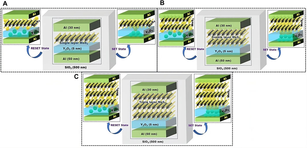
Figure 1. 3D structure of 2D MoS2 integrated thin Y2O3-based memristive device integrated with (A) single layer MoS2, (B) double layer MoS2, and (C) triple layer MoS2. Insets of each section show the SET and RESET operations wherein the dominant resistive switching mechanism is the formation and rupture of the CFs.
The thermodynamic numerical analysis model that was used relies on the principle of minimizing free energy (FE) within a memristive device, as FE varies under the influence of an external voltage. Simultaneously, the device reduces its free energy by utilizing phase transitions in the oxide material, involving the breaking of chemical bonds. This free energy within a memristive device is expressed as follows (Niraula and Karpov, 2017):
Herein, ρ: mass density of materials used in memristive structure, Cp: specific heat capacity of materials used in memristive structure at constant pressure, δT: change in temperature due to variations in thermal gradient inside the device, ε: permittivity of the active materials utilized in the memristive device, E: electric field, r: radius of conductive filament (CF), h: CF height in SET process, l: gap length in the case of RESET process, σs: interfacial energy, and δμ: difference in chemical potential between unstable conductive phase and insulating phase in SET process (δμ1) and between unstable conductive phase and metastable conductive phase in RESET process (δμ2) (Niraula and Karpov, 2017; Niraula and Karpov, 2018).
Eq. 1 delineates thermal and electrostatic energies in its first and second terms, respectively. The latter two terms correspond to phase transformation energy. Notably, the electrostatic energy stemming from the conductive elements (electrodes and filament) is marginal compared to the insulating layer, which possesses higher capacitance. Consequently, the insulator layer predominantly influences the overall free energy. Conversely, the thermal contribution is primarily driven by the conducting filament facilitating current flow between the top and bottom electrodes.
This work utilizes the following algorithmic steps to determine the device’s minimum free energy configuration and its corresponding current-voltage (I-V) characteristics: (a) Construct the device. (b) Apply a source voltage and compute the device’s free energy for varying filament radii. (c) Determine the change in free energy (∂F/∂r) corresponding to filament radius and gap length (∂F/∂l) for a constant source voltage. (d) Repeat steps (b) and (c) for different source voltages. (e) Record the device voltage, current, filament radius, filament gap length, and their respective minimum free energies for all source voltages. (f) Finally, obtain two sets of current-voltage (I-V) characteristics in step (e) pertaining to the SET and RESET processes.
The SET process comprises two key sub-processes: the rapid shunting of electrodes and the radial expansion of conductive filaments (CFs). Within the shunting phase, there are distinct stages: nucleation and longitudinal growth of CFs, both characterized by their stochastic behaviour (Gaba et al., 2013). Likewise, the RESET process consists of two fundamental sub-processes: the initiation of a gap through CF rupturing, followed by the stochastic growth of this gap.
2.2 COMSOL multiphysics modules
Figures 1A–C depicts the 3D schematic of the memristive devices used to build the 2D axisymmetric model in COMSOL for the SET and RESET processes. Leveraging a 2D geometry in COMSOL facilitates the reduction of volume integrals in Equation 1 to area integrals. The area integrals directly corresponding to the SET and RESET processes in COMSOL are expressed as (Niraula and Karpov, 2017; Niraula and Karpov, 2018):
In COMSOL modelling, the values of electric field (E) and temperature (T) can be determined by solving a set of partial differential equations, as presented below:
[i] Electric current module:
[ii] Heat transfer module (in solid):
[iii] Multiphysics module:
Herein, J: current density, σ: electric conductivity, κ: thermal conductivity and Qs: heat source. These equations are typically integrated into their corresponding COMSOL modules and extended for numerical modelling purposes.
Equations (4.1-4.3) establish the current conservation law, Ohm’s law, and the relationship between electric field and electric potential derived from Maxwell’s law, respectively. Eq. 5 represents the Fourier heat law, with the Joule heat term from Equation 6 providing the heat source. Detailed descriptions of the boundary conditions and electrical configurations employed during modelling are provided elsewhere (Kumar et al., 2024).
In this modelling approach, internal Joule heating and non-uniform electric field distribution within the memristive device are taken into account. Additionally, the study distinctly illustrates how the number of MoS2 layers impacts the device’s switching voltage and synaptic weight, characterized by potentiation (P) and depression (D), which constitutes the core concept of the research. The coefficients of the differential equations, including (4.1) to (4.3), (5), and (6), as well as the free energy equations 2 and (3) employed in this physical electro-thermal modelling, are provided in Table 1. Herein, the phonon assisted hopping mechanism is used through the optimum hopping chains. Additionally, the material non-crystallinity is one of the most common features of filamentary RRAM structures. In a non-crystalline material, some atoms or groups of atoms retain a certain mobility being able to move between two equilibrium positions which is described in terms of double well potential (DWP) as discussed in our previous report (Kumar et al., 2024).
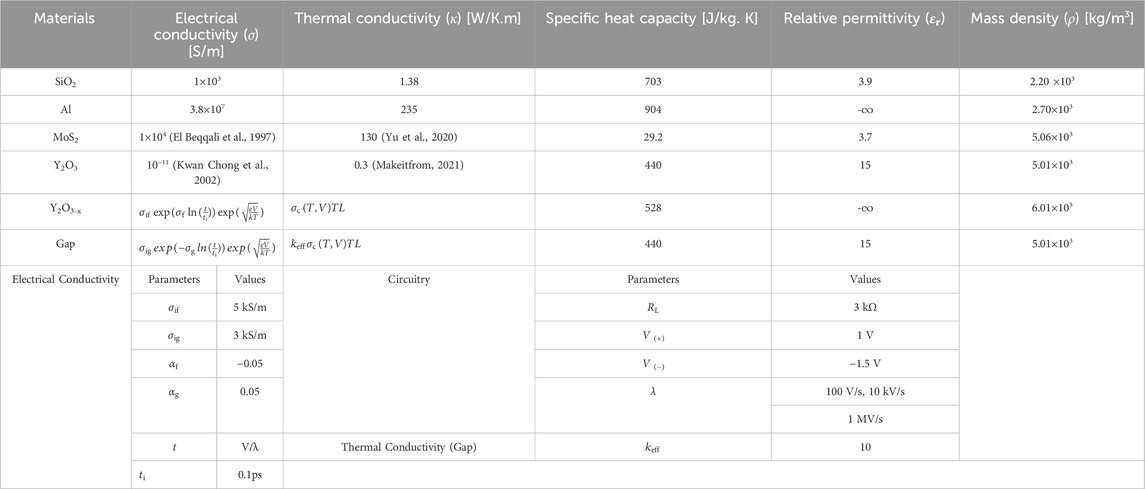
Table 1. Values of the coefficients of the differential equations and FE used in this physical electro-thermal modelling.
3 Results and discussion
Figure 2A illustrates the simulated RS behaviour of the 2D MoS2 integrated thin Y2O3-based memristive device subjected to a voltage pulsing scheme in the range −1.5 V to +1 V in forward and reverse bias, delivered to the top electrode through a load resistance. The RS response is segmented into four phases: positive forming voltage (+VF), positive SET voltage (VSET), negative rupture voltage (-VR), and negative RESET voltage (VRESET).
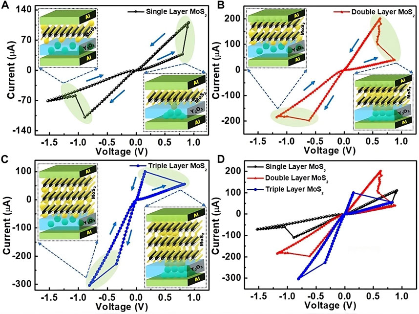
Figure 2. I-V characteristics depicting resistive switching response of the 2D MoS2 integrated thin Y2O3-based memristive device for (A) single layer MoS2, (B) double layer MoS2, (C) triple layer MoS2, and (D) comparative analysis of resistive switching response with number of MoS2 layers.
During the formation process, all CFs are created within the MoS2 and Y2O3 layer of the RS device, causing it to transition into the SET state when subjected to a voltage amplitude equal to or less than VF (as illustrated in Figure 2A). For the single layer MoS2 integrated Y2O3-based memristive device, VF and VSET are modelled to be +0.81 V and +0.91 V, respectively. Conversely, during the rupturing process, all previously formed CFs are disrupted, leading the memristive device to switch into the RESET state when exposed to a voltage amplitude equal to or less than -VR. The modelled values for -VR and VRESET are −1.5 V and −0.89 V, respectively, while in the case of double layer MoS2 with thin Y2O3 (shown in Figure 2B), the VF is +0.83 V, VSET is 0.62 V, -VR is −1.18 V and VRESET is −0.61 V. Subsequently, in triple layer MoS2 (shown in Figure 2C), the VF is +0.88 V, VSET is 0.15 V, -VR is −0.81 V and VRESET is −0.34 V. From Figures 3A,B it is concluded that the SET and RESET voltage values decrease as the number of 2D MoS2 monolayers increases. This proves that the presence of 2D MOS2 plays a pivotal role in the switching process, as compared to primary metal oxide layer. It is well known that the 2D MoS2 layer requires lower bias potential to switch the device in SET and RESET region, because it shows quantum confinement effect and high carrier mobility (Ling et al., 2023). Therefore, charge carriers can move more easily within the material under the influence of a lower electric field, facilitating faster switching at lower bias potentials. This attribute further enhances the low power computation capability of the presented memristive device structure (Xu et al., 2019).
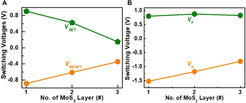
Figure 3. Impact of the number of 2D MoS2 layers in thin Y2O3-based memristive device over the switching voltages (A) VSET and VRESET, and (B) VF and VR. The lines are guide to the eye.
Additionally, to demonstrate the synaptic plasticity characteristics of the memristive device, such as potentiation and depression, a series of positive and negative voltage pulses with an amplitude of ±1 V and a voltage rise rate (VRR) of 100 V/s are administered to the device. Figure 4 shows the potentiation and depression functionality of single layer MoS2 (Figure 4A), double layer MoS2 (Figure 4B) and triple layer MoS2 (Figure 4C). As depicted in Figure 4A, when subjected to positive voltage pulses, the synaptic weight or normalized conductance of the memristive device undergoes a continuous reinforcement. Conversely, in response to negative electrical stimuli the synaptic weight diminishes. This ongoing modulation of the device’s conductance closely mimics the synaptic plasticity mechanisms observed in the brain (Jo et al., 2010; Das et al., 2018).
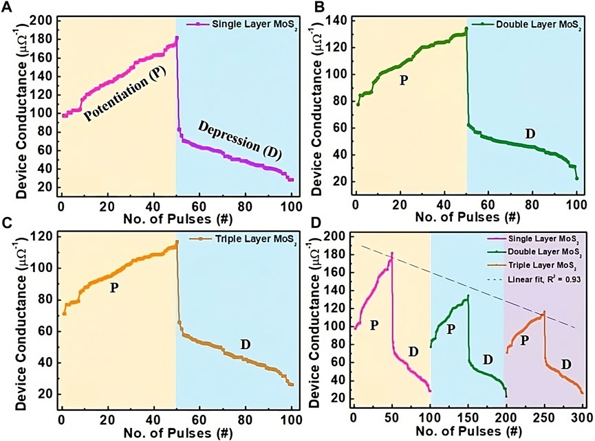
Figure 4. Impact of the number of 2D MoS2 layers in thin Y2O3-based memristive device over the device conductance (i.e., synaptic weight) for (A) single layer MoS2, (B) double layer MoS2, (C) triple layer MoS2, and (D) comparative analysis in the change of device conductance with number of MoS2 layers.
As evident from Figure 4D, the synaptic weight (or device conductance) of the memristive device is linearly decreased with an increment in the number of MoS2 layers within the device structure. It should be noted that in monolayer (∼0.65 nm thickness) MoS2, quantum confinement effects are more pronounced due to the atomic layer thickness of the material, resulting in enhanced carrier mobility (Ling et al., 2023). However, as the number of layers increases, these effects diminish, leading to reduced carrier mobility as well as conductivity. Additionally, this trend may be attributed to alterations in the lateral dimensions of the device. Moreover, in configurations with a higher number of MoS2 layers, the role of the thin metal oxide layer in the switching process diminishes, with primary switching being predominantly influenced by the MoS2 layers rather than the Y2O3 layer, which basically constitutes combination of interfacial and filamentary switching mechanism (Wang et al., 2016; Li et al., 2018; Ginnaram and Maikap, 2021; Pam et al., 2022). This shift in dominance significantly impacts the overall conductance of the device. In this study, a series of 100 identical pulses (comprising 50 positive and 50 negative pulses) with an amplitude of ±1 V and a pulse width of 10 ms are employed to analyse the synaptic characteristics. Consistent with findings in existing literature (Zhang et al., 2013; Jang et al., 2014; Liu et al., 2018; Kim et al., 2020), the metal/metal oxide interfaces demonstrate a gradual potentiation process and an abrupt depression process, as illustrated in Figure 4D. The sudden shift observed during the depression process is attributed to variations in the free energy at metal/metal oxide interfaces (Yu, 2017). Additionally, accounting for the metal/metal oxide free energy and induced oxide layer, non-identical spike pulses featuring varying pulse amplitudes or durations offer a potential solution to mitigate the high asymmetry ratio observed in potentiation and depression processes (Yu, 2017). However, employing non-identical spikes may introduce complexity to peripheral circuits and neuro-inspired computing systems (Yu, 2017).
Figure 5 depicts the impact of pulse amplitude on synaptic plasticity, delineating both potentiation and depression processes. The graphs illustrate how altering the pulse amplitude effectively modulates the device conductance for single (Figure 5A), double (Figure 5B) and triple layer MoS2 (Figure 5A), akin to the way spikes in neural communication influence synaptic strength. Notably, successive potentiation spikes elevate memristive conductance, while subsequent depression spikes induce a cycle of conductance reduction. The different pulsing scheme (non-identical pulses) is utilized during the computation of Figure 5. Maldonado et al (Maldonado et al., 2023) have observed similar behaviour experimentally in HfO2-based memristive devices. Therefore, considering the aforementioned analysis, it can be concluded that control over the MoS2 number of layers affects the conductance but not the synaptic response of the Yttria-based memristive device.
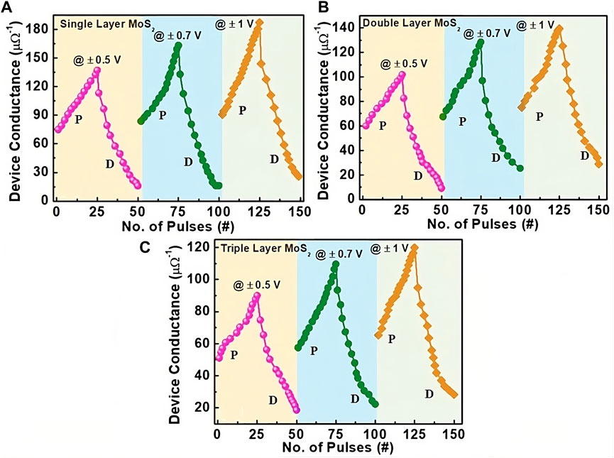
Figure 5. Synaptic plasticity, potentiation, and depression events in the memristive device under the application of varying pulsing scheme (non-volatile states) for (A) single layer MoS2, (B) double layer MoS2, and (C) triple layer MoS2.
4 Conclusion
We presented a physical model detailing the integration of a number of nanoscales 2D MoS2 layers with a thin metal oxide-based memristive device, aimed at emulating artificial synapse functionalities. The simulations demonstrate a bipolar RS response across all different number of MoS2 layers, with device switching voltages decreasing as the number of MoS2 layers increases. This phenomenon enhances the feasibility of 2D materials combined with transition metal oxide-based memristive devices in low-power computing applications. Moreover, the MoS2-modified memristive device structure successfully demonstrated synaptic plasticity in terms of potentiation and depression, while the device conductance can also be varied by tuning the amplitude of the input pulsing scheme. Notably, in monolayer MoS2, quantum confinement effects are more dominant due to the atomic layer thickness of the material, resulting in enhanced carrier mobility and corresponding increment in the device conductance. Conversely, in double and triple-layer MoS2, these effects are minimized, which further affects the synaptic response of the device. However, in double and tri-layer device structures, the bulk materials conductivity may play a more important role, affecting thus the device switching voltages more significantly, as compared to the overall effect on device conductance. Moreover, the modified memristive device structure with the integration of 2D MoS2 can pave the way for optoelectronic memories development that may also act as optoelectronic synapses in bionic visual applications. Hence, the profound advantage of the herein presented physical model lies in its ability to inform researchers about the potential functionalities of MoS2 integrated Y2O3-based memristive devices and guide them in developing novel low computing power 2D-TMD/TMO-based artificial synapses for tuneable neuromorphic computing applications.
Data availability statement
The original contributions presented in the study are included in the article/Supplementary material, further inquiries can be directed to the corresponding authors.
Author contributions
MG: Conceptualization, Data curation, Formal Analysis, Methodology, Software, Validation, Writing–review and editing. SR: Formal Analysis, Investigation, Visualization, Writing–review and editing. IZ: Funding acquisition, Investigation, Project administration, Resources, Software, Supervision, Visualization, Writing–review and editing. DG: Formal Analysis, Funding acquisition, Investigation, Project administration, Resources, Supervision, Validation, Visualization, Writing–review and editing. SK: Conceptualization, Data curation, Formal Analysis, Investigation, Methodology, Supervision, Validation, Visualization, Writing–original draft, Writing–review and editing.
Funding
The author(s) declare that no financial support was received for the research, authorship, and/or publication of this article.
Acknowledgments
The authors would like to thank the Indian Science Technology and Engineering Facilities Map (I-STEM), IISc, Bengaluru, India, and the University of Southampton, United Kingdom, for providing license for COMSOL® Multiphysics. SK would like to thank Department of Science and Technology (DST), New Delhi for research grant via IFA23-ENG-375. The support of the UK’s Engineering and Physical Science Research Centre is gratefully acknowledged, through EP/N00762X/1 and EP/X016730/1. MKG would like to thank National Overseas Scholarship (File No.: K-11015/100/2023-SCD-V-(NOS)). DGG acknowledges support from the UKRI Future Leaders Fellowship Grant (MR/V024442/1).
Conflict of interest
The authors declare that the research was conducted in the absence of any commercial or financial relationships that could be construed as a potential conflict of interest.
The author(s) declared that they were an editorial board member of Frontiers, at the time of submission. This had no impact on the peer review process and the final decision.
Publisher’s note
All claims expressed in this article are solely those of the authors and do not necessarily represent those of their affiliated organizations, or those of the publisher, the editors and the reviewers. Any product that may be evaluated in this article, or claim that may be made by its manufacturer, is not guaranteed or endorsed by the publisher.
References
Alshaya, A., Han, Q., and Papavassiliou, C. (2022). “RRAM, device, model and memory,” in International Conference on Microelectronics (ICM), Casablanca, Morocco, December, 2022.
Bocquet, M., Deleruyelle, D., Aziza, H., Muller, C., Portal, J. M., Cabout, T., et al. (2014). Robust compact model for bipolar oxide-based resistive switching memories. IEEE Trans. Electron Devices 61 (3), 674–681. doi:10.1109/TED.2013.2296793
Cao, Q., Xiong, L., Yuan, X., Li, P., Wu, J., Bi, H., et al. (2022). Resistive switching behavior of the memristor based on WS2 nanosheets and polyvinylpyrrolidone nanocomposites. Appl. Phys. Lett. 120, 232105. doi:10.1063/5.0087862
Das, M., Kumar, A., Singh, R., Htay, M. T., and Mukherjee, S. (2018). Realization of synaptic learning and memory functions in Y2O3 based memristive device fabricated by dual ion beam sputtering. Nanotechnology 29, 055203–055209. doi:10.1088/1361-6528/aaa0eb
Duan, H., Wang, D., Gou, J., Guo, F., Jie, W., and Hao, J. (2023). Memristors based on 2D MoSe2 nanosheets as artificial synapses and nociceptors for neuromorphic computing. Nanoscale 15, 10089–10096. doi:10.1039/D3NR01301D
El Beqqali, O., Zorkani, I., Rogemond, F., Chermette, H., Ben Chaabane, R., Gamoudi, M., et al. (1997). Electrical properties of molybdenum disulfide MoS2: experimental study and density functional calculation results. Synth. Met. 90 (3), 165–172. doi:10.1016/S0379-6779(98)80002-7
Feng, X., Li, Y., Wang, L., Chen, S., Yu, Z. G., Tan, W. C., et al. (2019). A fully printed flexible MoS2 memristive artificial synapse with femtojoule switching energy. Adv. Electron Mater 5, 1900740. doi:10.1002/aelm.201900740
Gaba, S., Sheridan, P., Zhou, J., Choi, S., and Lu, W. (2013). Stochastic memristive devices for computing and neuromorphic applications. Nanoscale 5, 5872. doi:10.1039/C3NR01176C
Gautam, M. K., Kumar, S., Chaudhary, S., Hindoliya, L. K., Kumbhar, D. D., Park, J. H., et al. (2023). Experimental validation of switching dependence of nanoscale-Y2O3 memristor on electrode symmetry via physical electro-thermal modeling. ACS Appl. Electron. Mater. 5 (7), 3885–3893. doi:10.1021/acsaelm.3c00598
Ge, R., Wu, X., Kim, M., Shi, J., Sonde, S., Tao, L., et al. (2018). Atomristor: nonvolatile resistance switching in atomic sheets of transition metal dichalcogenides. Nano Lett. 18, 434–441. doi:10.1021/acs.nanolett.7b04342
Ginnaram, S., and Maikap, S. (2021). Memristive and artificial synapse performance by using TiOx/Al2O3 interface engineering in MoS2-based metallic filament memory. J. Phys. Chem. Solids 151, 109901. doi:10.1016/j.jpcs.2020.109901
Ielmini, D. (2016). Resistive switching memories based on metal oxides: mechanisms, reliability and scaling. Semicond. Sci. Technol. 31 (6), 063002. doi:10.1088/0268-1242/31/6/063002
Jang, J. W., Park, S., Jeong, Y. H., and Hwang, H. (2014). “ReRAM-based synaptic device for neuromorphic computing,” in 2014 IEEE International Symposium on Circuits and Systems (ISCAS), Melbourne, VIC, Australia, June, 2014.
Jin, S., Kwon, J. D., Kim, Y., Jin, S., Kwon, J. D., and Kim, Y. (2021). Statistical analysis of uniform switching characteristics of Ta2O5-based memristors by embedding in-situ grown 2D-MoS2 buffer layers. Materials 14 (21), 6275. doi:10.3390/ma14216275
Jo, S. H., Chang, T., Ebong, I., Bhadviya, B., Mazumder, P., and Lu, W. (2010). Nanoscale memristor device as synapse in neuromorphic systems. Nano Lett. 10 (4), 1297–1301. doi:10.1021/nl904092h
Kim, K., Park, S., Hu, S. M., Song, J., Lim, W., Jeong, Y., et al. (2020). Enhanced analog synaptic behavior of SiNx/a-Si bilayer memristors through Ge implantation. NPG Asia Mater. 12 (77), 77. doi:10.1038/s41427-020-00261-0
Kim, M., Ge, R., Wu, X., Lan, X., Tice, J., Lee, J. C., et al. (2018). Zero-static power radio-frequency switches based on MoS2 atomristors. Nat. Commun. 9 (2524), 2524. doi:10.1038/s41467-018-04934-x
Kim, M., Rehman, M. A., Lee, D., Wang, Y., Lim, D. H., Khan, M. F., et al. (2022). Filamentary and interface-type memristors based on tantalum oxide for energy-efficient neuromorphic hardware. ACS Appl. Mat. Interfaces 14 (39), 44561–44571. doi:10.1021/acsami.2c12296
Kim, S., Kim, S. J., Kim, K. M., Lee, S. R., Chang, M., Cho, E., et al. (2013a). Physical electro-thermal model of resistive switching in bi-layered resistance-change memory. Sci. Rep. 3 (1680), 1680. doi:10.1038/srep01680
Kim, S., Kim, S. J., Kim, K. M., Lee, S. R., Chang, M., Cho, E., et al. (2013b). Physical electro-thermal model of resistive switching in bi-layered resistance-change memory. Sci. Rep. 3 (1680), 1680. doi:10.1038/srep01680
Korotcenkov, G., and Cho, B. K., The role of grain size on the thermal instability of nanostructured metal oxides used in gas sensor applications and approaches for grain-size stabilization, vol. , 58, no. 4, 2012, pp. 167–208. doi:10.1016/j.pcrysgrow.2012.07.001
Kumar, S., Agarwal, A., and Mukherjee, S. (2022b). Electrical performance of large-area Y2O3 memristive crossbar array with ultralow C2C variability. IEEE Trans. Electron Devices 69 (7), 3660–3666. doi:10.1109/TED.2022.3172400
Kumar, S., Das, M., Htay, M. T., Sriram, S., and Mukherjee, S. (2022c). Electroforming-free Y2O3 memristive crossbar array with low variability. ACS Appl. Electron. Mater. 4 (6), 3080–3087. doi:10.1021/acsaelm.2c00472
Kumar, S., Dubey, M., Nawaria, M., Gautam, M. K., Das, M., Bhardwaj, R., et al. (2024). Investigation of filament formation and surface perturbation in nanoscale-Y2O3 memristor: a physical modelling approach. J. Electron. Mater., doi:10.1007/s11664-024-10967-4
Kumar, S., Gautam, M. K., Gill, G. S., and Mukherjee, S. (2022d). 3-D physical electro-thermal modelling of nanoscale Y2O3 memristors for synaptic application. IEEE Trans. Electron Devices 69 (6), 3124–3129. doi:10.1109/TED.2022.3166858
Kumar, S., Gautam, M. K., Yadav, S., and Mukherjee, S. (2023). Memcapacitive to memristive transition in Al/Y2O3/GZO crossbar array. IEEE Trans. Electron Devices 70 (6), 3341–3346. doi:10.1109/TED.2023.3265622
Kumar, S., Kumbhar, D. D., Park, J. H., Kamat, R. K., Dongale, T. D., and Mukherjee, S. (2022a). Y2O3-Based crossbar array for analog and neuromorphic computation. IEEE Trans. Electron Devices 70 (2), 473–477. doi:10.1109/TED.2022.3227890
Kumbhar, D. D., Kumar, S., Dubey, M., Kumar, A., Dongale, T. D., Pawar, S. D., et al. (2024). Exploring statistical approaches for accessing the reliability of Y2O3-based memristive devices. Microelectron. Eng. 288, 112166. doi:10.1016/j.mee.2024.112166
Kwan Chong, R., Seong Woo, Y., Byung You, H., Yong Han, R., Jin Mo, K., and Dong Geun, J. (2002). Structural and electrical properties of yttrium oxide with tungsten gate. J. Korean Phys. Soc. 40 (1), 103–106. Available at: https://inis.iaea.org/search/search.aspx?orig_q=RN:33056693.
Li, D., Wu, B., Zhu, X., Wang, J., Ryu, B., Lu, W. D., et al. (2018). MoS2 memristors exhibiting variable switching characteristics toward biorealistic synaptic emulation. ACS Nano 12 (9), 9240–9252. doi:10.1021/acsnano.8b03977
Li, R., Wang, W., Li, Y., Gao, S., Yue, W., and Shen, G. (2023). Multi-modulated optoelectronic memristor based on Ga2O3/MoS2 heterojunction for bionic synapses and artificial visual system. Nano Energy 111, 108398. doi:10.1016/j.nanoen.2023.108398
Li, S., Pam, M. E., Li, Y., Chen, L., Chien, Y. C., Fong, X., et al. (2022). Wafer-scale 2D hafnium diselenide based memristor crossbar array for energy-efficient neural network hardware. Adv. Mater 34, 2103376. doi:10.1002/adma.202103376
Lin, Y., Wang, W., Li, R., Kim, J., Zhang, C., Kan, H., et al. (2024). Multifunctional optoelectronic memristor based on CeO2/MoS2 heterojunction for advanced artificial synapses and bionic visual system with nociceptive sensing. Nano Energy 121, 109267. doi:10.1016/j.nanoen.2024.109267
Ling, Y., Li, J., Luo, T., Lin, Y., Zhang, G., Shou, M., et al. (2023). MoS2-Based memristor: robust resistive switching behavior and reliable biological synapse emulation. Nanomaterials 13 (3117), 3117. doi:10.3390/nano13243117
Liu, H., Wei, M., and Chen, Y. (2018). Optimization of non-linear conductance modulation based on metal oxide memristors. Nanotechnol. Rev. 5 (7), 443–468. doi:10.1515/ntrev-2018-0045
Lu, X. F., Zhang, Y., Wang, N., Luo, S., Peng, K., Wang, L., et al. (2021). Exploring low power and ultrafast memristor on p-type van der Waals SnS. Nano Lett. 21 (20), 8800–8807. doi:10.1021/acs.nanolett.1c03169
Luo, R., Xu, W. W., Zhang, Y., Wang, Z., Wang, X., Gao, Y., et al. (2020). Van der Waals interfacial reconstruction in monolayer transition-metal dichalcogenides and gold heterojunctions. Nat. Commun. 11 (1), 1011. doi:10.1038/s41467-020-14753-8
Makeitfrom (2021). Yttria (yttrium oxide, Y2O3). Available at: https://www.makeitfrom.com/material-properties/Yttria-Yttrium-Oxide-Y2O3.
Maldonado, D., Cantudo, A., Perez, E., Zaliz, R. R., Quesada, E. P. B., Mahadevaiah, M. K., et al. (2023). TiN/Ti/HfO2/TiN memristive devices for neuromorphic computing: from synaptic plasticity to stochastic resonance. Front. Neurosci. 17, 1271956. doi:10.3389/fnins.2023.1271956
Marseglia, E. A. (1983). Transition metal dichalcogenides and their intercalates. Int. Rev. Phys. Chem. 3 (2), 177–216. doi:10.1080/01442358309353343
Naqi, M., Kang, M. S., liu, N., Kim, T., Baek, S., Bala, A., et al. (2022). Multilevel artificial electronic synaptic device of direct grown robust MoS2 based memristor array for in-memory deep neural network. npj 2D Mater Appl. 6 (53), 53. doi:10.1038/s41699-022-00325-5
Niraula, D., and Karpov, V. (2017). “Numerical modeling of resistive switching in RRAM device,” in Proceedings of the 2017 COMSOL Conference in Boston, Boston, MA, USA, October, 2017.
Niraula, D., and Karpov, V. (2018). Comprehensive numerical modeling of filamentary RRAM devices including voltage ramp-rate and cycle-to-cycle variations. J. Appl. Phys. 124 (17). doi:10.1063/1.5042789
Pam, M. E., Li, S., Su, T., Chien, Y. C., Li, Y., Ang, Y. S., et al. (2022). Interface-Modulated resistive switching in Mo-irradiated ReS2 for neuromorphic computing. Adv. Mater. 34 (30), e2202722. doi:10.1002/adma.202202722
Peng, B., Zhang, H., Shao, H., Xu, Y., Zhang, X., and Zhu, H. (2016). Thermal conductivity of monolayer MoS2, MoSe2, and WS2: interplay of mass effect, interatomic bonding and anharmonicity. RSC Adv. 6, 5767–5773. doi:10.1039/C5RA19747C
Pickett, M. D., Strukov, D. B., Borghetti, J. L., Yang, J. J., Snider, G. S., Stewart, D. R., et al. (2009). Switching dynamics in titanium dioxide memristive devices. J. Appl. Phys. 106 (7). doi:10.1063/1.3236506
Ranganathan, K., Raz, M. F., and Ismach, A. (2020). Large-scale and robust multifunctional vertically aligned MoS2 photomemristors. Adv. Funct. Mater 30, 2005718. doi:10.1002/adfm.202005718
Sangwan, V. K., Jariwala, D., Kim, I. S., Chen, K. S., Marks, T. J., Lauhon, L. J., et al. (2015). Gate-tunable memristive phenomena mediated by grain boundaries in single-layer MoS2. Nat. Nanotech 10, 403–406. doi:10.1038/nnano.2015.56
Sato, H., Shima, H., Nokami, T., Itoh, T., Honma, Y., Naitoh, Y., et al. (2021). Memristors with controllable data volatility by loading metal ion-added ionic liquids. Front. Nanotechnol. 3. doi:10.3389/fnano.2021.660563
Strukov, D. B., Snider, G. S., Stewart, D. R., and Williams, R. S. (2008). The missing memristor found. Nature 453, 80–83. doi:10.1038/nature06932
Tong, W., and Liu, Y. (2023). Recent progress of layered memristors based on two-dimensional MoS2. Sci. China 66, 160402–160402:10. doi:10.1007/s11432-023-3751-y
Traore, B., Blaise, P., Vianello, E., Perniola, L., Salvo, B. D., and Nishi, Y. (2016). HfO2-based RRAM: electrode effects, Ti/HfO2 interface, charge injection, and oxygen (O) defects diffusion through experiment and ab initio calculations. IEEE Trans. Electron Devices 63 (1), 360–368. doi:10.1109/TED.2015.2503145
Wang, W., Panin, G. N., Fu, X., Zhang, L., Ilanchezhiyan, P., Pelenovich, V. O., et al. (2016). MoS2 memristor with photoresistive switching. Sci. Rep. 6, 31224. doi:10.1038/srep31224
Wang, X. F., Tian, H., Zhao, H. M., Zhang, T. Y., Mao, W. Q., Qiao, Y. C., et al. (2018). Interface engineering with MoS2-Pd nanoparticles hybrid structure for a low voltage resistive switching memory. Small 14 (2). doi:10.1002/smll.201702525
Wang, Y., Gong, Y., Huang, S., Xing, X., Lv, Z., Wang, J., et al. (2021). Memristor-based biomimetic compound eye for real-time collision detection. Nat. Commun. 12 (5979), 5979. doi:10.1038/s41467-021-26314-8
Wang, Z., Joshi, S., Savel’ev, S. E., Jiang, H., Midya, R., Lin, P., et al. (2017). Memristors with diffusive dynamics as synaptic emulators for neuromorphic computing. Nat. Mater 16, 101–108. doi:10.1038/nmat4756
Wu, F., Si, S., Cao, P., Wei, W., Zhao, X., Shi, T., et al. (2019). Interface engineering via MoS2 insertion layer for improving resistive switching of conductive-bridging random access memory. Adv. Electron. Mater. 5 (4). doi:10.1002/aelm.201800747
Xia, Q., and Yang, J. J. (2019). Memristive crossbar arrays for brain-inspired computing. Nat. Mater 18, 309–323. doi:10.1038/s41563-019-0291-x
Xu, R., Jang, H., Lee, M. H., Amanov, D., Cho, Y., Kim, H., et al. (2019). Vertical MoS2 double-layer memristor with electrochemical metallization as an atomic-scale synapse with switching thresholds approaching 100 mV. Nano Lett. 19 (4), 2411–2417. doi:10.1021/acs.nanolett.8b05140
Yan, X., Zhao, Q., Chen, A. P., Zhao, J., Zhou, Z., Wang, J., et al. (2019). Vacancy-induced synaptic behavior in 2D WS2 nanosheet-based memristor for low-power neuromorphic computing. Small 15, 1901423. doi:10.1002/smll.201901423
Yang, J. J., Strukov, D. B., and Stewart, D. R. (2013). Memristive devices for computing. Nat. Nanotech 8, 13–24. doi:10.1038/nnano.2012.240
Yin, X., Tang, C. S., Wu, D., Kong, W., Li, C., Wang, Q., et al. (2019). 2D transition metal dichalcogenide: unraveling high-yield phase-transition dynamics in transition metal dichalcogenides on metallic substrates (adv. Sci. 7/2019). Adv. Sci. 6 (7), 1802093. doi:10.1002/advs.201802093
Yu, S. (2017). Neuro-inspired computing using resistive synaptic devices. Berlin, Germany: Springer. ISBN 978-3-319-54313-0. doi:10.1007/978-3-319-54313-0
Yu, Y., Minhaj, T., Huang, L., Yu, Y., and Cao, L. (2020). In-plane and interfacial thermal conduction of two-dimensional transition-metal dichalcogenides. Phys. Rev. Appl. 13, 034059. doi:10.1103/PhysRevApplied.13.034059
Zhang, J. J., Sun, H. J., Li, Y., Wang, Q., Xu, X. H., and Miao, X. S. (2013). AgInSbTe memristor with gradual resistance tuning. Appl. Phys. Lett. 102 (18). doi:10.1063/1.4804983
Keywords: 2D-TMD materials, metal oxide materials, layered integration, memristive devices, artificial synapses
Citation: Gautam MK, Kumar S, Rani S, Zeimpekis I and Georgiadou DG (2024) 2D MoS2 monolayers integration with metal oxide-based artificial synapses. Front. Nanotechnol. 6:1400666. doi: 10.3389/fnano.2024.1400666
Received: 14 March 2024; Accepted: 16 April 2024;
Published: 29 April 2024.
Edited by:
Dayanand Kumar, King Abdullah University of Science and Technology, Saudi ArabiaReviewed by:
Rohit Abraham John, ASM America, Inc, United StatesMahesh Chougale, Queensland University of Technology, Australia
Swapnil R. Patil, Jeju National University, Republic of Korea
Copyright © 2024 Gautam, Kumar, Rani, Zeimpekis and Georgiadou. This is an open-access article distributed under the terms of the Creative Commons Attribution License (CC BY). The use, distribution or reproduction in other forums is permitted, provided the original author(s) and the copyright owner(s) are credited and that the original publication in this journal is cited, in accordance with accepted academic practice. No use, distribution or reproduction is permitted which does not comply with these terms.
*Correspondence: Sanjay Kumar, c2FuamF5c2loYWc5MUBnbWFpbC5jb20=; Dimitra G. Georgiadou, RC5HZW9yZ2lhZG91QHNvdG9uLmFjLnVr
†These authors have contributed equally to this work and share first authorship