 Sachin Maheshwari
 Alex Serb
 Themis Prodromakis
- Centre for Electronics Frontiers, Institute for Integrated Micro Nano Systems, School of Engineering, University of Edinburgh, Edinburgh, United Kingdom
Due to their high density, scalability, and low-power properties, 1-transistor-1-resistor (1T1R) RRAM-based crossbars have been exploited in the past. However, the series resistance of the transistor is a major problem in 1T1R crossbar arrays. This limits the maximum current available for inducing resistive switching and degrades the array’s performance. To mitigate this issue, we propose a new configuration—1-transistor-1-diode-1-resistor (1T1D1R)—in which diodes are used (including bulk source/drain parasitic diodes of the access transistor) to bypass the gating transistor during the programming operation (“write”). The proposed solution trades increased overhead in the layout area for a dramatic increase in the maximum achievable current drive on RRAM devices, resulting in the ability to deliver 1.5 mA+ with a voltage supply as low as 1.2 V using minimum-size devices (in our implementation). We designed a 32 × 32 crossbar array with on-chip peripheral circuitry in commercially available 0.18 μm triple-well CMOS technology for the proof of concept. We demonstrate bidirectional programming, showing a memristance change of ≈500 Ω for 120 and 80 pulses in positive and negative directions, respectively.
1 Introduction
With the evolution of data-intensive applications, from machine learning (ML) to deep learning (DL) (LeCun et al., 2015), processing and storing large amounts of data are the biggest challenges for the Von Neumann architecture. The Von Neumann bottleneck arises due to the long access time per operation in fetching both instructions and data from memory via a single bus. It thus limits the overall performance of a system, dissipating a large amount of energy. To solve this technological bottleneck, the emergence of non-volatile memory (NVM) became a new paradigm, with technologies that offer promising features over classical memory technologies, such as high density, low leakage power, scalability, and computing-in-memory (CIM) capabilities (Staudigl et al., 2022). There are numerous NVM technologies, including resistive random-access memory (RRAM), phase change memory (PCM), spin-transfer-torque magnetic RAM (STT-MRAM), and ferroelectric field effect transistors (FeFETs). Some have even become commercially available, such as TSMC’s 40 nm RRAM (Chou et al., 2018) and Intel’s 22 nm RRAM (Jain et al., 2019), TSMC’s 40 nm PCM (Wu et al., 2018), Intel’s 22 nm STT-MRAM (Wei et al., 2019), and Samsung’s 28 nm STT-MRAM (Song et al., 2018), while doped
Numerous studies have been conducted on the design of memory cells without using NVM technologies. Kim (2008) designed a single-bit memory cell using bipolar transistors, external Schottky diodes, and a capacitor. It was characterized by a lower word line loading, as it bypasses the transistors during programming. Prabhat and Myers (2020) demonstrate the use of the body bias technique to accommodate SRAM cells to operate at a lower operating voltage. Other SRAM-based designs also exist that use body bias technology to increase power efficiency (Mishra et al., 2021; Faraji et al., 2014). Houghton et al. (1998) designed a gain cell in a memory array using two transistors, one diode, and one capacitor. The main focus of their design is the gain cells used for the read-out operation and the diodes that prevent the conduction of the read transistor in the opposite direction.
RRAM/Memristor is considered a game-changing electronic device that can store multi-bit information at extremely low operational power (Stathopoulos et al., 2017; Chen et al., 2020). Moreover, due to its scalability, fast switching speed, and excellent cmos compatibility, it is considered competitive in next-generation memory devices (Berdan et al., 2014; Guan et al., 2012; Yu et al., 2012). RRAM-based crossbar arrays have been widely studied for in-memory computing and neuromorphic applications for their benefits in speeding computation and high area efficiency (Majhi et al., 2017; Lee et al., 2007). However, “raw” arrays suffer from “sneak current”, also known as “sneak path current,” whereby undesirable current flows through unselected or non-intended memory cells. This is demonstrated in Figure 1, where the green dotted path is the selected cell, while the red path results from unselected cells. Thus, the power which inherently compromises measurement accuracy in resistance states is drained, possibly even causing unintended writing on unselected cells. Multiple solutions exist, both at the biasing scheme and device levels. Biasing schemes (Chen, 2013; Deng et al., 2013; Li et al., 2021), effective at large write and read voltages, constrain leakage by applying some intermediate voltages to all the unselected cells within the array, thus preventing undesired disturbance to the stored data. Very recently, Chen et al. (2024) demonstrated that enhancing self-rectifying behavior in memristive cells offers better performance by characterizing the sneak path current in passive crossbar arrays. However, the dominant solution currently for circuit designers is using a selector— also known as an “access device”—connected in the path of the RRAM device, giving rise to the 1-selector-1-RRAM (1S1R) configuration. The selector may be a diode (1-diode-1-RRAM; 1D1R), a transistor (1-transistor-1-RRAM; 1T1R), or a mixed-ionic–electronic–conduction (MIEC) selector (Li et al., 2021; Huang et al., 2011; Burr et al., 2012; Chen et al., 2023). Transistor selectors are popular because they are directly implementable in cmos and have extra control flexibility via gate signaling. However, transistor selectors also bottleneck the high scalability of RRAM into high-density crossbar arrays and introduce significant series resistance, requiring compensation in the form of higher write voltages applied across the 1T1R stack. Dinh et al. (2016) used one transistor, one diode, and one RRAM to design a memory device. Here, the access transistor was switched on during programming and reading, while the parasitic diode was used during the erase mode. While this approach is interesting, the transistors’ series resistance is a major bottleneck. Additionally, this approach cannot be used for bi-directional programming and multi-bit read–write at low voltages. Alshaya et al. (2023) and Fouda et al. (2018) found that the switching time for the 1T1R configuration is high and increases as the crossbar size increases.
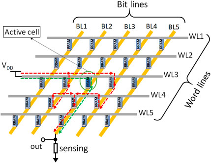
Figure 1. RRAM-based
To circumvent this, a new cell structure—1-transistor-1-diode-1-resistor (1T1D1R) uses metal oxide-semiconductor (MOS) diodes, including the bulk-S
We have thus far successfully validated the 1T1D1R cell in the 0.18
2 1T1D1R memory cell design and operations
We propose a 1T1D1R structure, a tileable “memory cell” that when placed in an array configuration, can perform three basic operations: a) bidirectional (a.k.a. bipolar) programming/write; b) read; c) low-power idle mode (park). The 1T1D1R cell shown in Figure 2 has six terminals. Two of these arise as the nmos transistor sits on an insulated substrate formed by a nested
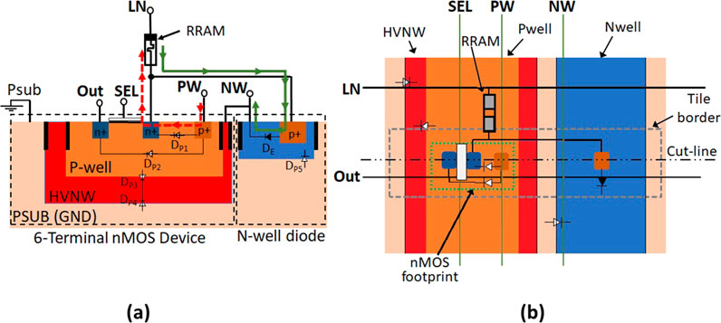
Figure 2. Layout view of 1T1D1R. (a) 2-D cross-section of 1T1D1R configuration along the cut line. Red dashed line and solid green line paths with arrows illustrate negative and positive programming directions, respectively. (b) Top view showing the nmos footprint.
The two Nwells are connected via metal layers, and the terminal is named “
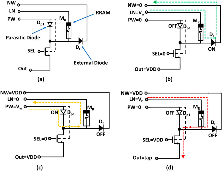
Figure 3. (a) 1T1D1R circuit diagram showing diodes and RRAM. (b–d) Terminal voltages for (b) “positive” programming with current direction from
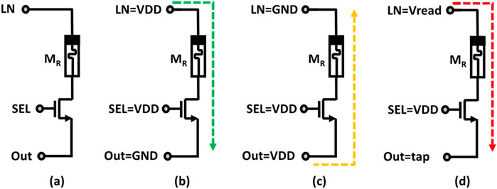
Figure 4. (a) Conventional 1T1R cell. Illustrates terminal voltages for (b) positive programming with the current direction from
2.1 Circuit operations
2.1.1 Programming mode
RRAM devices store data in their resistive states. Frequently, a “1” is stored as a suitably defined low resistive state (LRS) and “0” as a high resistive state (HRS). However, to program either of these values, potentially significant current must be passed through the RRAM device or “stuck-at” faults may occur.
In programming mode, terminal
2.1.2 Read mode
For the read operation, the proposed 1T1D1R configuration maintains backward compatibility with standard 1T1R and offers multiple options. In all cases,
2.1.3 Park mode
The memristors in the memory array are used as memory storage elements and are therefore electrically reconfigurable (they can be toggled repeatedly between their low and high conductance states called OFF and ON). There are several ways to “park” this circuit (switch it off). A possible configuration is with
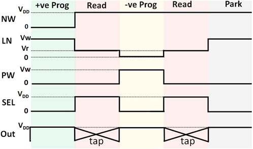
Figure 5. Timing diagram for programming (positive and negative), reading, and park operations.
2.2 Array design: no sneak current path
Here we examine the behavior of a
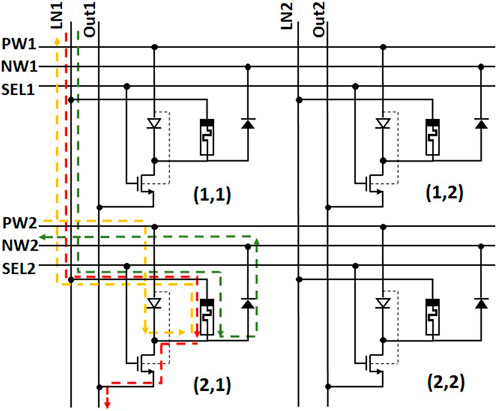
Figure 6. Programming and read paths of the target cell (2,1) in a
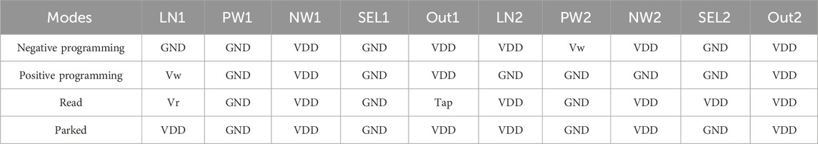
Table 1. Voltage levels for the operation of a (2,1) target cell in a
3 Memristor and 1T1D1R cell response
3.1 Memristor characteristics
Multiple memristor models exist in the literature (Kvatinsky et al., 2015; Messaris et al., 2017; Messaris and Serb, 2018). For this study, we use our in-house fabricated valance change memory (VCM) metal–insulator–metal structure
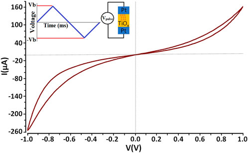
Figure 7. Typical I-V characteristic showing the pinched hysteresis loop of our in-house fabricated memristor model. The inset shows the test bench and the input voltage. The model’s parameters are presented in the appendix of Maheshwari et al. (2021a).
3.2 1T1D1R versus 1T1R under DC and transient response
RRAM device programming in both forward (positive) and reverse directions (negative) is done by setting the terminals
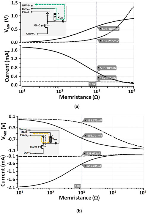
Figure 8. Current and voltage drive
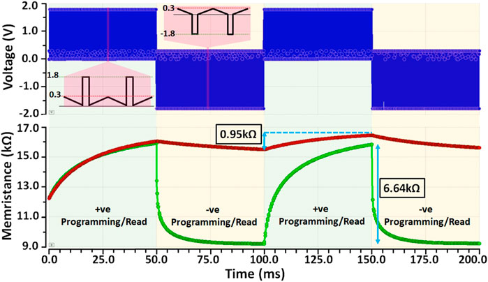
Figure 9. 1T1D1R versus 1T1R transient response for programming and read pulse width of 1
4 32 × 32 crossbar array design and analysis
4.1 Architecture design overview
For proof-of-concept, we designed a
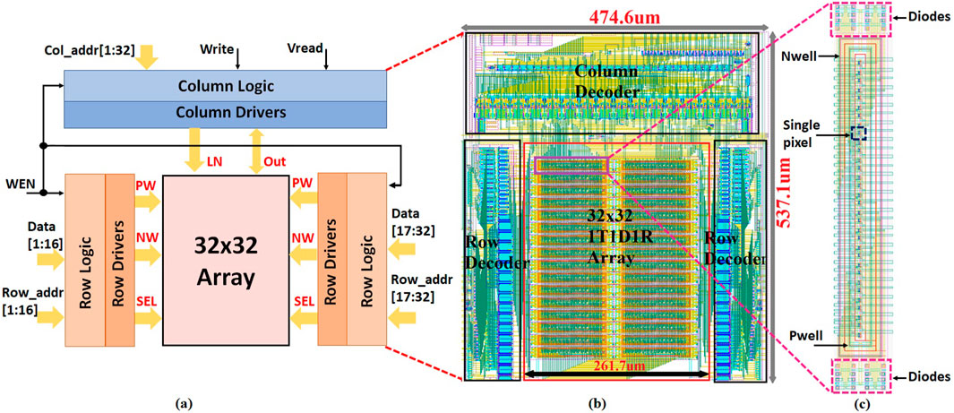
Figure 10. (a)
The target cell is selected based on the row (
4.1.1 32 × 32 array design
To minimize the crossbar area, 32 nmos transistors are encapsulated inside
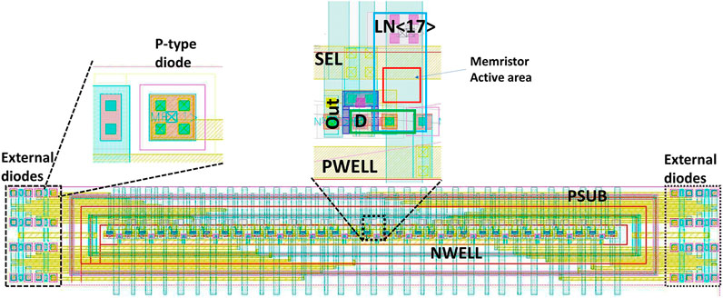
Figure 11. Layout of a
4.1.2 Row circuitry
The row circuitry (RC) constitutes logic for
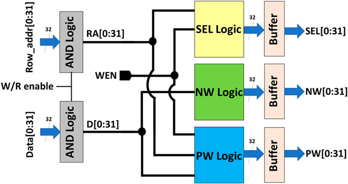
Figure 12. Implementation of 32 × 32 row circuitry, used to generate row signals SEL, NW, and PW. Input address and data are gated with a write/read enable signal.
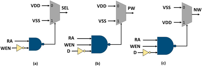
Figure 13. Gate-level implementation showing row logic circuitry. (a) SEL logic set either to VDD or GND. (b) Pwell logic used for negative programming. (c) Nwell logic used for positive programming.
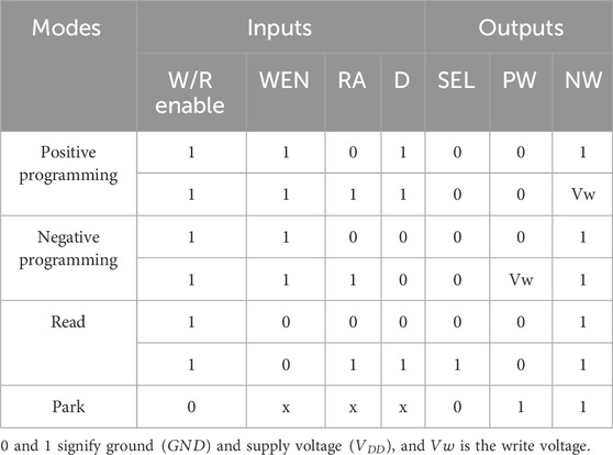
Table 2. Row logic circuitry truth table generating SEL, PW, and NW signals for positive programming, negative programming, read, and park mode.
4.1.3 Column circuitry
The column circuitry (CC) constitutes logic for
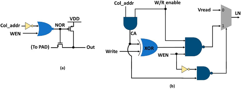
Figure 14. Column circuitry for reading either single cell or bunch of cells, either row or column-wise. (a) Out-logic for reading stored value in a cell. (b) LN logic for setting required voltage for writing and reading.
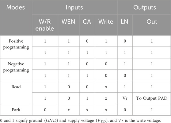
Table 3. Column logic circuitry truth table generating LN and Out signals for positive programming, negative programming, read, and park mode.
4.2 Timing analysis and evaluation
The post-layout simulated waveform for the
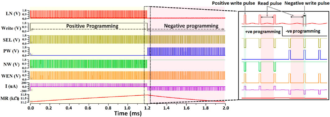
Figure 15. Post-layout simulated results for 32 × 32 cells with peripheral circuits. Write and read pulse widths are 1
The final comparison of 1T1D1R with 1T1R cell is shown in Table 4. Due to the two wells, the cell has a higher area; however, there is a negligible change in the programming energy consumption. The proposed design shows an increased current drive, recorded at 1 k
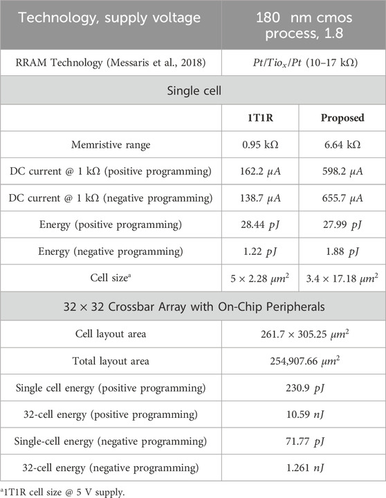
Table 4. Comparison of 1T1R and proposed 1T1D1R single cell and post layout result of
5 Discussion and conclusion
We obtained a
Data availability statement
The original contributions presented in the study are included in the article/supplementary material; further inquiries can be directed to the corresponding author.
Author contributions
SM: Conceptualization, Formal Analysis, Investigation, Methodology, Validation, Writing – original draft, writing – review and editing. AS: Conceptualization, Project Administration, Supervision, Visualization, Writing – review and editing. TP: Conceptualization, Funding acquisition, Supervision, Writing – review and editing.
Funding
The author(s) declare that financial support was received for the research and/or publication of this article. This work was supported by the Engineering and Physical Sciences Research Council (EPSRC) Research Grant EP/R024642/1-2 (codename FORTE) and the Royal Academy of Engineering Chair in Emerging Technologies under Grant CiET1819/2/93.
Conflict of interest
The authors declare that the research was conducted in the absence of any commercial or financial relationships that could be construed as a potential conflict of interest.
Generative AI statement
The author(s) declare that no Generative AI was used in the creation of this manuscript.
Publisher’s note
All claims expressed in this article are solely those of the authors and do not necessarily represent those of their affiliated organizations, or those of the publisher, the editors and the reviewers. Any product that may be evaluated in this article, or claim that may be made by its manufacturer, is not guaranteed or endorsed by the publisher.
References
Alshaya, A., Malik, A., Mifsud, A., and Papavassiliou, C. (2023). Comparison of 1T1R and 1C1R ReRAM arrays. J. Physics:Conf. Ser. 2613, 012010. doi:10.1088/1742-6596/2613/1/012010
Berdan, R., Lim, C., Khiat, A., Papavassiliou, C., and Prodromakis, T. (2014). A memristor spice model accounting for volatile characteristics of practical reram. IEEE Electron Device Lett. 35, 135–137. doi:10.1109/LED.2013.2291158
Boni, A., Malena, F., Saccani, F., Amoretti, M., and Caselli, M. (2023). Boosting RRAM-based mixed-signal accelerators in FD-SOI technology for ML applications. IEEE J. Explor. Solid-State Comput. Devices Circuits 9, 159–167. doi:10.1109/JXCDC.2023.3309713
Burr, G. W., Virwani, K., Shenoy, R. S., Padilla, A., BrightSky, M., Joseph, E. A., et al. (2012). “Large-scale (512kbit) integration of multilayer-ready access-devices based on mixed-ionic-electronic-conduction (miec) at 100% yield,” in 2012 symposium on VLSI technology, 41–42. doi:10.1109/VLSIT.2012.6242451
Chen, A. (2013). A comprehensive crossbar array model with solutions for line resistance and nonlinear device characteristics. IEEE Trans. Electron Devices 60, 1318–1326. doi:10.1109/ted.2013.2246791
Chen, J., Wu, H., Gao, B., Tang, J., Hu, X. S., and Qian, H. (2020). A parallel multibit programing scheme with high precision for rram-based neuromorphic systems. IEEE Trans. Electron Devices 67, 2213–2217. doi:10.1109/TED.2020.2979606
Chen, P.-H., Su, Y.-T., Huang, W.-C., and Wu, C.-W. (2023). Improving high resistance state in one-transistor-one-resistor (1t1r) structure resistance random access memory with a body-biased method. IEEE Trans. Electron Devices 70, 1014–1018. doi:10.1109/TED.2023.3236316
Chen, Z., Zhao, X., Bengel, C., Liu, F., Li, K., Menzel, S., et al. (2024). Assessment of functional performance in self-rectifying passive crossbar arrays utilizing sneak path current. Sci. Rep. 14, 24682. doi:10.1038/s41598-024-74667-z
Chou, C. C., Lin, Z. J., Tseng, P. L., Li, C. F., Chang, C. Y., Chen, W. C., et al. (2018). “An n40 256k× 44 embedded rram macro with sl-precharge sa and low-voltage current limiter to improve read and write performance,” in 2018 IEEE international solid - state circuits conference - (ISSCC), 478–480. doi:10.1109/ISSCC.2018.8310392
Deng, Y., Huang, P., Chen, B., Yang, X., Gao, B., Wang, J., et al. (2013). Rram crossbar array with cell selection device: a device and circuit interaction study. IEEE Trans. Electron Devices 60, 719–726. doi:10.1109/TED.2012.2231683
Dinh, J., Gopinath, V. P., Gonzales, N., Lewis, D., Kamalanathan, D., and Kwan, M. S. (2016). Resistive switching Memory having a resistor, diode, and switch memory cell adesto technologies corporation. Sunnyvale, CA. (US): US 9.530.495 B1).
Dünkel, S., Trentzsch, M., Richter, R., Moll, P., Fuchs, C., Gehring, O., et al. (2017). A fefet based super-low-power ultra-fast embedded nvm technology for 22nm fdsoi and beyond. IEEE Inter Electron Devices Meet. 19, 7.1–19.7.4. doi:10.1109/IEDM.2017.8268425
Faraji, R., Naji, H. R., Rahimi-Nezhad, M., and Arabnejhad, M. (2014). New sram design using body bias technique for low-power and high-speed applications. Int. J. Circuit Theory Appl. 42, 1189–1202. doi:10.1002/cta.1914
Fouda, M. E., Eltawil, A. M., and Kurdahi, F. (2018). Modeling and analysis of passive switching crossbar arrays. IEEE Trans. Circuits Syst. I Regul. Pap. 65, 270–282. doi:10.1109/TCSI.2017.2714101
Guan, X., Yu, S., and Wong, H.-S. P. (2012). On the switching parameter variation of metal-oxide rram—part i: Physical modeling and simulation methodology. IEEE Trans. Electron Devices 59, 1172–1182. doi:10.1109/ted.2012.2184545
Houghton, R. J., Bertin, C. L., Fifield, J. A., Miller, C. P., and Tonti, W. R. (1998). Gain memory cell with diode, 5. Armonk, N.Y.: International Business Machines Corporation, 757–693.
Huang, J.-J., Tseng, Y.-M., Luo, W.-C., Hsu, C.-W., and Hou, T.-H. (2011). One selector-one resistor (1s1r) crossbar array for high-density flexible memory applications. 2011 Int. Electron Devices Meet. 31 (7), 1–31.7.4. doi:10.1109/IEDM.2011.6131653
Jain, P., Arslan, U., Sekhar, M., Lin, B. C., Wei, L., Sahu, T., et al. (2019). “13.2 a 3.6mb 10.1mb/mm2 embedded non-volatile reram macro in 22nm finfet technology with adaptive forming/set/reset schemes yielding down to 0.5v with sensing time of 5ns at 0.7v,” in IEEE international solid-state circuits conference, 212–214. doi:10.1109/ISSCC.2019.8662393
Kvatinsky, S., Ramadan, M., Friedman, E. G., and Kolodny, A. (2015). VTEAM:A general model for voltage-controlled memristors. IEEE Trans. Circuits Syst. II 62, 786–790. doi:10.1109/tcsii.2015.2433536
LeCun, Y., Bengio, Y., and Hinton, G. (2015). Deep learning. Nature 521, 436–444. doi:10.1038/nature14539
Lee, M.-J., Park, Y., Kang, B.-S., Ahn, S.-E., Lee, C., Kim, K., et al. (2007). “2-stack 1d-1r cross-point structure with oxide diodes as switch elements for high density resistance ram applications,” in 2007 IEEE international electron devices meeting, 771–774. doi:10.1109/IEDM.2007.4419061
Li, H., Wang, S., Zhang, X., Wang, W., Yang, R., Sun, Z., et al. (2021). Memristive crossbar arrays for storage and computing applications. Adv. Intell. Syst. 3, 2100017. doi:10.1002/aisy.202100017
Maheshwari, S., Stathopoulos, S., Wang, J., Serb, A., Pan, Y., Mifsud, A., et al. (2021a). Design flow for hybrid cmos/memristor systems—part i: modeling and verification steps. IEEE Trans. Circuits Syst. I Regul. Pap. 68, 4862–4875. doi:10.1109/TCSI.2021.3122343
Maheshwari, S., Stathopoulos, S., Wang, J., Serb, A., Pan, Y., Mifsud, A., et al. (2021b). Design flow for hybrid cmos/memristor systems—part ii: circuit schematics and layout. IEEE Trans. Circuits Syst. I Regul. Pap. 68, 4876–4888. doi:10.1109/TCSI.2021.3122381
Majhi, P., Karpov, E. V., Pillarisetty, R., Shah, U., Mukherjee, N., and Clarke, J. S. (2017). 1T1R RRAM architecture adesto technologies corporation. Sunnyvale, CA. (US): WO2017171780A1).
Messaris, I., Nikolaidis, S., Serb, A., Stathopoulos, S., Gupta, I., Khiat, A., et al. (2017). “A tio2 reram parameter extraction method,” in 2017 IEEE international symposium on circuits and systems, 1–4. doi:10.1109/ISCAS.2017.8050789
Messaris, I., Serb, A., Stathopoulos, S., Khiat, A., Nikolaidis, S., and Prodromakis, T. (2018). A data-driven verilog-a reram model. IEEE Trans. Computer-Aided Des. Integr. Circuits Syst. 37, 3151–3162. doi:10.1109/TCAD.2018.2791468
Mifsud, A., Shen, J., Feng, P., Xie, L., Wang, C., Pan, Y., et al. (2022). “A cmos-based characterisation platform for emerging rram technologies,” in IEEE international symposium on circuits and systems, 1–5.
Mishra, J. K., Upadhyay, B. B., Misra, P. K., and Goswami, M. (2021). Design and analysis of sram cell using body bias controller for low power applications. Circuits Syst. Signal Process 40, 2135–2158. doi:10.1007/s00034-020-01578-5
Prabhat, P., and Myers, J. E. (2020). Periphery body Biasing for memory applications arm limited, cambridge (GB): us 10, 586, 790–B2.
Slipko, V. A., and Pershin, Y. V. (2021). Importance of the window function choice for the predictive modelling of memristors. IEEE Trans. Circuits Syst. II Express Briefs 68, 2167–2171. doi:10.1109/TCSII.2019.2906295
Song, Y. J., Lee, J. H., Han, S. H., Shin, H. C., Lee, K. H., Suh, K., et al. (2018). Demonstration of highly manufacturable stt-mram embedded in 28nm logic. IEEE Int. Electron Devices Meet. 18, 2.1–18.2.4. doi:10.1109/IEDM.2018.8614635
Stathopoulos, S., Khiat, A., Trapatseli, M., Cortese, S., Serb, A., Valov, I., et al. (2017). Multibit memory operation of metal-oxide bi-layer memristors. Sci. Rep. 7, 17532. doi:10.1038/s41598-017-17785-1
Staudigl, F., Merchant, F., and Leupers, R. (2022). A survey of neuromorphic computing-in-memory: architectures, simulators, and security. IEEE Des. and Test 39, 90–99. doi:10.1109/MDAT.2021.3102013
Wei, L., Alzate, J. G., Arslan, U., Brockman, J., Das, N., Fischer, K., et al. (2019). “13.3 a 7mb stt-mram in 22ffl finfet technology with 4ns read sensing time at 0.9v using write-verify-write scheme and offset-cancellation sensing technique,” in 2019 IEEE international solid- state circuits conference - (ISSCC), 214–216. doi:10.1109/ISSCC.2019.8662444
Wu, J., Chen, Y., Khwa, W. S., Yu, S. M., Wang, T. Y., Tseng, J., et al. (2018). A 40nm low-power logic compatible phase change memory technology. 2018 IEEE Int. Electron Devices Meet. (IEDM) 27.6, 1–27.6.4. doi:10.1109/IEDM.2018.8614513
Keywords: crossbar array, low voltage, RRAM, 1T1R, parasitic diode, programming, selector technologies
Citation: Maheshwari S, Serb A and Prodromakis T (2025) Low-voltage programming of RRAM-based crossbar arrays using MOS parasitic diodes. Front. Nanotechnol. 7:1587700. doi: 10.3389/fnano.2025.1587700
Received: 04 March 2025; Accepted: 02 May 2025;
Published: 03 July 2025.
Edited by:
Syed Arshad Hussain, Tripura University, IndiaReviewed by:
Ziang Chen, Friedrich Schiller University Jena, GermanySherin Thomas, Indian Institute of Technology Ropar, India
Sarappadi Narasimha Prasad, Manipal Institute of Technology Bengaluru, India
Copyright © 2025 Maheshwari, Serb and Prodromakis. This is an open-access article distributed under the terms of the Creative Commons Attribution License (CC BY). The use, distribution or reproduction in other forums is permitted, provided the original author(s) and the copyright owner(s) are credited and that the original publication in this journal is cited, in accordance with accepted academic practice. No use, distribution or reproduction is permitted which does not comply with these terms.
*Correspondence: Sachin Maheshwari, bWFoZXNod2FyaS5zYWNoaW5AZWQuYWMudWs=