 Santhosh Sivasubramani
 Themis Prodromakis
- Centre for Electronic Frontiers, Institute for Integrated Micro and Nano Systems, School of Engineering, The University of Edinburgh, Edinburgh, United Kingdom
Artificial Intelligence (AI) is revolutionizing industries worldwide, delivering unprecedented productivity gains across diverse sectors, from healthcare to manufacturing. Recent advances in generative AI models have particularly accelerated innovation, enabling more efficient execution of complex tasks such as drug discovery, autonomous driving, and predictive maintenance. In the areas of electronics manufacturing: a sector crucial to the advancement of modern technologies, the impact of AI is profound, with the potential to transform every stage of the supply chain. This perspective investigates the role of AI in reshaping the electronics and semiconductor industries, exploring how it integrates into various stages of production and development. The approach to AI integration is structured and methodical, addressing both challenges and opportunities across five key nanotechnology areas: materials discovery, device design, circuit and system design, testing/verification, and modeling. In materials discovery, AI aids in identifying new, more efficient and sustainable materials. In device design, it enhances the functionality and integration of components. AI’s capabilities in circuit and system design enables more complex and precise electronic systems. During the testing and verification stage, AI contributes to more rigorous and faster testing processes, ensuring reliability before market release. Finally, in modeling, AI’s predictive capabilities allow for accurate simulations, crucial for anticipating performance under various scenarios. Each pillar of this electronics supply chain underscores AI’s ability to accelerate processes, optimize performance, and reduce costs. Supported by case studies of AI-driven breakthroughs, this perspective provides a comprehensive review of current AI applications across the entire electronic supply chain, illustrating improvements in yield and sustainable manufacturing practices.
1 Introduction
AI is rapidly transforming science and technology by enhancing productivity, improving decision-making, and optimizing complex systems across a wide range of domains. In software development, tools like GitHub Copilot and ChatGPT are reshaping how code is written and reviewed, boosting efficiency and reducing cognitive load for developers (Noy and Zhang, 2023; Weber et al., 2024; Bird et al., 2023; Ziegler et al., 2024). Similar gains are evident in finance (Humaid et al., 2024) and public services (Henman, 2020), where AI supports tasks from fraud detection to policy design, including critical areas such as cybersecurity (Kroll et al., 2021). Furthermore, AI is enabling breakthroughs in clean energy (Chen et al., 2023), precision medicine (Tan et al., 2023; Heydari et al., 2024; Serov and Vinogradov, 2022; Gholap et al., 2024; Liu et al., 2021), and agriculture (Zhang et al., 2021). These advances are driven by innovations such as predictive modeling for nanomaterials, personalized drug delivery systems, and data-driven approaches to crop optimization. These advancements also bring challenges, such as managing complex datasets and modeling nanoscale systems. Additionally, AI’s integration into public sector workflows prompts broader discussions on ethics, transparency, and human development (Ardichvili, 2022; Tong et al., 2021).
Building on these broader advancements, particularly in nanomaterials and system-level optimization, AI is increasingly influencing nanoelectronics, where it supports innovations across material characterization, device optimization, and advanced manufacturing processes. In material characterization, AI techniques are crucial for ensuring that properties meet specific device requirements, as demonstrated by (Botifoll et al., 2022), exploring AI’s role in nanomaterial characterization and electron microscopy for advanced nanocharacterization. In terms of device design and optimization, (Xu et al., 2023), illustrate how AI enhances the functionality and sensitivity of wearable electronics like electronic skin, while (Khailany, 2020) highlight AI’s automation of semiconductor device design processes. The manufacturing industry also benefits from AI, with (Papadimitriou et al., 2024; Konstantopoulos et al., 2022; Arinez et al., 2020) discussing its role in materials design, nanomaterial manufacturing, and advanced manufacturing techniques, which lead to more efficient and less wasteful production methods. AI’s predictive capabilities are leveraged for thermal management and optimizing power efficiency in densely packed electronic devices, as shown by (Basu et al., 2024; Zhao et al., 2020). Optoelectronic technologies also benefit from AI, with (Chen et al., 2022), and (Piccinotti et al., 2020) enhancing the design and functionality of optical components integral to sensors and communication modules. Furthermore, AI plays a significant role in energy storage for portable electronics, as (Lombardo et al., 2021) discuss its application in developing more efficient battery solutions. The advancements in AI-driven nano-electronics, set the stage for a deeper integration of these technologies into the broader electronics supply chain.
The electronics supply chain is a complex and multifaceted industry, structured around five critical pillars: material discovery, device design, circuits and system design, testing and verification, and modeling, which collectively support the development, production, and distribution of high-quality electronic systems. As illustrated in Figure 1, these pillars are integrated with centralized artificial intelligence, forming a closed-loop framework where six interconnected components, including an optimization engine that continuously refines the design of experiments based on prior outcomes, enhance efficiency and innovation across the supply chain. Material discovery focuses on the research and development of new materials that enhance the performance, durability, and efficiency of electronic devices, leading to innovations in semiconductors. Device design is crucial for determining the physical and functional characteristics of components like transistors and capacitors, optimizing their performance within electronic circuits. In circuits and system design, these components are integrated into coherent systems that meet specific functional requirements while ensuring reliability. Testing and verification ensure that every component and system meets rigorous standards for reliability and safety, identifying potential failures and design flaws before mass production. Lastly, modeling involve creating virtual replicas of physical devices or systems to simulate real-world behavior, allowing designers to predict performance and identify issues without physical prototypes, thereby speeding up development and reducing costs. Together, these pillars form a robust framework supporting innovation and efficiency in the electronics supply chain, facilitating the seamless delivery of electronic products to the market. Understanding these complex nature of the electronics supply chain provides a foundational backdrop for this paper, which emerges into how AI-driven methodologies are specifically transforming the field of nanoelectronics.
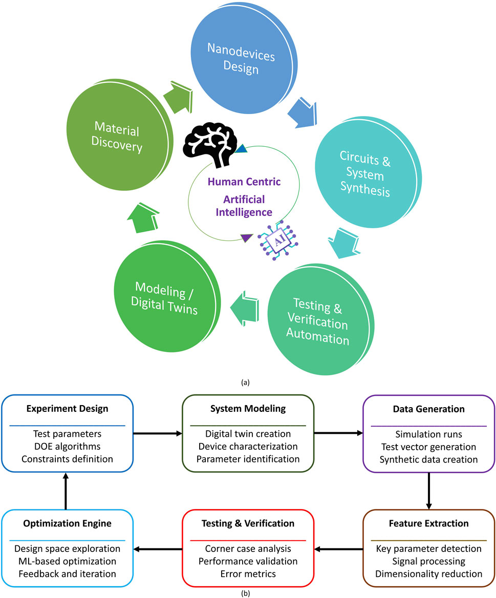
Figure 1. (a) Five key pillars encompassing the electronic supply chain centered by human centric artificial intelligence (b) This block diagram illustrates a complete automated design of experiments system for digital domain applications with six key components.
As a result, this paper presents a structured perspective on the latest advancements. Section 2 covers AI for synthesizing electronic materials, where machine learning models facilitate the discovery and optimization of nanomaterials by predicting material properties, identifying novel compounds, and refining synthesis processes. These AI-driven approaches reduce reliance on the need for costly trial-and-error experimentation, accelerating material development. Section 3 covers AI for optimizing nanodevice architectures, focusing on how AI enhances nanodevice design by refining physical and electrical characteristics, optimizing transistor performance, sensor sensitivity, and memory efficiency. Advanced algorithms improve scalability and energy efficiency, addressing key design constraints. Section 4 covers AI for automating the synthesis of circuits and systems. Given the complexity of nanoelectronic circuits, AI-powered tools aid in circuit layout generation, performance validation, and verification, facilitating the development of highly integrated and reliable electronic systems. Section 5 covers AI for aiding the testing and verification of nanoelectronics, where AI-driven methodologies improve fault detection, enhance test coverage, and predict failure mechanisms, thereby reducing manufacturing costs and improving device robustness. Section 6 covers AI for the development of digital twins for semiconductors. AI supports the creation of virtual models of nanoelectronic systems that enable real-time monitoring, predictive analysis, and performance optimization. These AI-enhanced simulations improve manufacturing precision and device lifecycle management. Finally, section 7 provides a future outlook, emphasizing the need for workforce development to address unresolved challenges.
2 AI for nanomaterials in electronics
The integration of AI into the synthesis of nanomaterials for electronics utilizes advanced algorithms to streamline synthesis processes, predict material properties, and minimize resource consumption and environmental impact. This section explores AI’s contributions to various aspects of nanomaterial synthesis as detailed in the forthcoming subsections.
2.1 Machine learning for property prediction and design
The application of machine learning in material science, particularly for property prediction and design, advances our ability to develop new materials and optimize existing ones with substantial precision. The use of machine learning algorithms enables the prediction of material properties and the design of new materials in ways that established methods cannot match.
Advancements in Material Science through ML: Data driven approach is changing the way materials are developed, characterized, and optimized, enabling to achieve breakthroughs at substantial speeds. For example, (Kadulkar et al., 2022), discusses how machine learning assists in the design of material properties, significantly reducing the dimensionality of design spaces and accelerating the process of material innovation. Similarly, (Lampe et al., 2023), highlights the rapid, data-efficient optimization of perovskite nanocrystal syntheses through the fusion of machine learning algorithms, which enhances the material properties with limited experimental data, showcasing the practical benefits of AI in synthesizing advanced materials. The drive towards discovering new materials is further advanced by (Cai et al., 2020), where machine learning algorithms play a pivotal role in uncovering new potential materials, thus expanding the boundaries of material science. The comprehensive application of AI across the whole life cycle of material discovery is explored by (Li Jiali et al., 2020), demonstrating how AI is integrated at every stage from synthesis to application, thereby enhancing the material development process. In addition, (Hei Chan et al., 2022), explores the application of machine learning for advanced material prediction and design, providing insights into how AI can be leveraged to predict material behaviors and properties accurately.
AI-Driven Innovations in Material Design and Synthesis: In the forefront of this development, (Xu et al., 2022; Badini et al., 2023), reviews the instantaneous property prediction and inverse design of plasmonic nanostructures using machine learning, highlighting current applications and future directions in nanoengineering. (Furxhi et al., 2024). provides a practical example of how machine learning is applied to the synthesis of silver nanoparticles, establishing design rules that optimize nanoparticle development based on synthesis parameters. These studies collectively underscore the substantial impact of machine learning on the field of material science, enabling more rapid, efficient, and innovative material discovery and design processes that are set to redefine the industry standards. (Batra et al., 2021), discusses the emergence of materials intelligence ecosystems driven by machine learning, illustrating how these systems integrate diverse datasets to accelerate innovation and discovery in material science. Furthermore, (Yang et al., 2022), provides a comprehensive review of computational, data-driven design of nanomaterials, highlighting how big data is utilized predicting material structures and properties, optimizing synthesis processes and material functionalities. The work by (Pollice et al., 2021) on data-driven strategies for accelerated materials design exemplifies the application of high-throughput virtual screening and inverse molecular design, techniques that leverage large datasets to rapidly prototype and refine materials. (Ahmadi et al., 2021), addresses the application of machine learning in the high-throughput experimental exploration of metal halide perovskites, demonstrating how AI streamlines the exploration of compositional space to enhance the performance of these materials significantly.
2.2 AI-driven synthesis optimization
The study by (Wang and Zhu, 2024) demonstrates the effectiveness of AI in optimizing online processes compared to established offline methods, achieving better resource efficiency and maintaining high-quality nanocrystal production. (Han et al., 2020), explores machine learning to optimize the synthesis of carbon dots, achieving higher quantum yields important for optoelectronics and bioimaging. The integration of Bayesian optimization and deep learning by (Mekki-Berrada et al., 2021) quickly produces nanoparticles with desired optical properties, demonstrating AI’s potential to accelerate and refine synthesis processes. Further advancements include (Vikram et al., 2021)’s use of neural networks for the accelerated screening of colloidal nanocrystals, effectively reducing the number of required experiments. The “Artificial Chemist,” an autonomous quantum dot synthesis bot introduced by (Epps et al., 2020), marks a step towards fully automated laboratories, speeding up material development with minimal human intervention. Additionally, (Price et al., 2024), highlights the predictive capabilities of machine learning in synthesizing nanomaterials, where key properties are predicted from small datasets, optimizing time and resource use. The combination of machine learning with microfluidics technology in a self-driving platform for metal nanoparticle synthesis by (Tao et al., 2021) dynamically optimizes reaction conditions, improving scalability and efficiency. (Epps et al., 2021), discusses the use of ensemble neural networks to optimize material synthesis in microfluidic systems, showing superior performance over known methods. Moreover, (Xu et al., 2024), employs neural networks to predict outcomes of hot injection quantum dot synthesis, providing insights that enable fine-tuning of synthesis parameters for optimal product quality. Lastly, a comprehensive review by (Gulevich et al., 2024) on machine learning-assisted colloidal synthesis encapsulates the broad spectrum of AI applications in this field, highlighting the advancements and efficiencies brought by machine learning techniques in optimizing colloidal nanomaterial synthesis. These studies collectively put-forth the role of AI in enhancing nanomaterial synthesis, offering improved efficiency and reduced environmental impact while opening new avenues.
2.3 Autonomous systems and robotics in material discovery
In parallel, the integration of AI with robotics in material discovery automates the entire process of material synthesis and discovery, leading towards the development of fully autonomous laboratories. This approach is exemplified by (Jiang et al., 2022), where an AI-enabled chemical synthesis robot, AI-EDISON, autonomously explores chemical spaces and optimizes nanomaterial synthesis, enhancing the precision and efficiency of material development. The development of closed-loop systems that integrate robotics with machine learning for continuous optimization of nanoparticle synthesis is discussed by (Park et al., 2023), enhancing throughput and consistency in production. Similarly, (Soldatov et al., 2021), discusses the implementation of self-driving laboratories that automate the synthesis and optimization of new functional materials, showing how AI can streamline complex chemical processes and accelerate material innovation. The convergence of AI and experimental automation in autonomous laboratories is further explored by (Xie Yunchao et al., 2023), which enhance the autonomy of material synthesis processes, thereby increasing throughput and reducing human intervention. Moreover, (Li Jiagen et al., 2020), explores into the use of Bayesian optimization in autonomous systems for materials synthesis, illustrating the synergy between AI and robotics in creating more efficient and responsive synthesis protocols. The concept of on-demand material synthesis is brought to life by (Szymanski et al., 2023), where collaborative robots and virtual reality are employed to enable autonomous materials synthesis and scientific discovery, pushing the boundaries of what is possible in materials science.
As we conclude this section, it is evident that AI technologies have significantly impacted the field of material science, particularly in the synthesis and design of materials for electronics. By automating synthesis processes, enhancing material properties, and reducing environmental impacts, AI is not only optimizing current methodologies but also paving the way for future discoveries. In the next section, we will understand how nanodevice designs are impacted by AI.
3 AI for optimising nanodevice design
AI is increasingly being integrated into the field of nanodevice design, significantly enhancing the capabilities of design and simulation processes. This integration leverages advanced machine learning algorithms to streamline and improve the accuracy of simulations, predict device behavior under various conditions, and optimize design parameters. AI’s role extends from the initial conceptual stages through to the detailed engineering phases, enabling faster development cycles and more efficient validation of nanodevices. This section explores how AI technologies are being applied to reshape established standard approaches in nanodevice architecture, focusing on design optimization, simulation enhancements, and predictive analysis.
3.1 AI-enhanced design and simulation in nanodevice architecture
The integration of AI into nanodevice architecture has significantly transformed the landscape as evident across various facets of semiconductor design, from conceptualization to the detailed predictive simulations that anticipate device behavior under diverse conditions.
AI-Driven Design Optimization: Studies such as those by (Cauwenberghs et al., 2023; Jeong et al., 2021) discuss AI’s role in enhancing the design of micro/nano circuits and systems. These technologies automate and refine processes that traditionally required extensive manual intervention and iterative testing. For instance, (Cheng et al., 2021), explores sensitivity prediction for VLSI technology development using ML, demonstrating how AI can expedite the development cycle by predicting outcomes based on design changes. AI’s ability to handle complex datasets enables the simulation of scenarios that are challenging to model using conventional methods. For example, (Wang et al., 2021; Wang et al., 2024) illustrate how AI models simulate advanced semiconductor devices, providing insights that guide the optimization of design parameters for enhanced performance. Additionally, (Aleksandrov et al., 2023a), describes a fully convolutional generative machine learning method for accelerating non-equilibrium Green’s function simulations, showcasing further advancements in simulation technologies facilitated by AI. Furthermore, semiconductor device geometry optimization has emerged as a crucial area where AI significantly enhances performance and efficiency. By intelligently exploring vast design spaces, AI-driven models identify optimal geometrical configurations that minimize power consumption, improve switching speed, and reduce heat generation.
Simulation and Predictive Analysis: AI extends into the simulation phase, aiding in predicting the physical and electronic properties of materials and devices. (Chen et al., 2024; Osowiecki et al., 2024; Manley et al., 2024) discuss AI in semiconductor process optimization, where predictive models forecast the outcomes of various manufacturing processes. This predictive capability is crucial for identifying optimal manufacturing conditions and reducing the time and cost associated with experimental trials. Additionally, AI facilitates the development of accurate models for electronic design automation (EDA). As noted by (Qiao et al., 2025), AI-driven tools enable the simulation of complex electronic systems, allowing designers to anticipate the performance of these systems in real-world applications. This is particularly important in the context of heterogeneous integration technologies, where different components must be seamlessly integrated into a single device. The studies by (Butola et al., 2022; Xiao Li et al., 2022) further emphasize the role of AI in enhancing the modeling and simulation of intrinsic parameter fluctuations and multiphysics digital twins, respectively, highlighting the breadth of AI applications in device simulation.
3.2 AI in process control and manufacturing
AI significantly impacts the manufacturing phase of nanodevices, enhancing both process control and operational efficiency.
Enhancing Process Control: AI-driven virtual metrology and process control systems, as discussed in (Maitra et al., 2024; Liu et al., 2025), predict defects and process deviations, enabling real-time corrective actions. This not only improves yield but also enhances the reliability of the manufacturing process. AI models assist in real-time monitoring and adjustment of manufacturing processes, optimizing the settings of manufacturing equipment, which is critical for maintaining the precision required in nanofabrication ((Lin et al., 2021; Ho et al., 2021)).
Manufacturing Efficiency: AI also plays a pivotal role in enhancing the overall efficiency of manufacturing processes. For example, (Gökgöz et al., 2024; Lai et al., 2023) highlight how AI algorithms optimize production lines and reduce waste, thereby improving both the speed and quality of manufacturing. The integration of AI into these processes ensures that nanodevice fabrication meets the high standards required for advanced applications.
3.3 AI for device characterization
AI contributes significantly to the characterization of nanodevices, particularly in analyzing and predicting material behavior and device performance.
Predictive Modeling and Characterization: AI models, such as those discussed in (Aleksandrov et al., 2023b; Hong et al., 2025), are used to model and analyze the behavior of materials at the nanoscale. These models provide valuable insights essential for improving device performance, predicting how materials will behave under different conditions, and identifying potential improvements in material properties.
Enhancing Device Reliability: AI-driven characterization tools also enhance the reliability of devices. By accurately predicting device failures and identifying potential quality issues before they become critical, AI systems save significant resources and time. This predictive maintenance capability leads to longer device lifespans and more reliable performance metrics, as demonstrated in studies like (Kim Min-Hwi et al., 2021; Gökgöz et al., 2024). The integration of AI across various stages of nanodevice architecture: from design and simulation to manufacturing and characterization, marks a significant advancement in the field. This integration not only enhances efficiency and accuracy but also paves the way for innovations that were previously unattainable, setting a new standard for the development of nanodevices. Next, we will explore how it impacts circuits.
4 AI for automating the synthesis of circuits and systems
The integration of AI into the synthesis and layout automation of circuits and systems has challenged EDA. This section examines two key aspects of AI applications in synthesis and layout automation inluding design and optimization techniques, reliability and performance evaluation. AI introduces new capabilities that streamline design workflows, improve accuracy, and reduce time-to-market, enabling engineers and designers to address complex design challenges more effectively.
4.1 AI-driven design and optimization techniques
AI has significantly evolved the efficiency and accuracy of circuit design and optimization processes. The review by (Fayazi et al., 2021) encapsulates AI’s applications in modeling and optimizing analog and mixed-signal circuits, focusing on automated circuit sizing and performance model accuracy improvements. (Zhao and Zhang, 2020), introduces an automated framework for topology synthesis in analog integrated circuits, enhancing design efficiency by generating and evaluating creative circuit topologies. (Li Jiagen et al., 2020), proposes an AI-based design approach for optimizing power converter circuit parameters, automating the design process that traditionally requires extensive human intervention. In the domain of approximate computing, (Zervakis et al., 2020), presents a framework for designing circuits with runtime reconfigurable accuracy to improve energy efficiency without compromising performance. (Khailany, 2020), explores the acceleration of chip design using AI to automate optimization tasks, transforming traditional workflows. The survey by (Scarabottolo et al., 2020) discusses the synthesis of approximate circuits, a method that relaxes accuracy requirements to achieve benefits in design area and power consumption. (Fayazi et al., 2023), introduces AnGeL, a neural network-assisted framework that significantly reduces the need for labeled data in analog circuit generation. (Senhora et al., 2022), explores topology optimization through a physics-based learning strategy, enhancing the design process without sacrificing accuracy.
The application of graph neural networks in high-level synthesis design space exploration is detailed by (Ferretti et al., 2022), which improves efficiency and prediction accuracy over established methods. (Carrion Schafer and Wang, 2019), provides a comprehensive look at the past, present, and future of high-level synthesis design space exploration, emphasizing the role of AI in exploring optimal hardware microarchitectures. The deep reinforcement learning approach by (Martins and Lourenço, 2023) for analog integrated circuit topology synthesis showcases significant improvements in handling large-scale designs and generating creative topologies. The comprehensive survey by (Chen et al., 2020) on EDA and graph neural networks highlights the integration of machine learning into various stages of the EDA flow, addressing time and resource constraints and enhancing solution quality. Lastly, (Lau Neto et al., 2022), discusses FlowTune, a framework that uses a domain-specific multiarmed bandit approach for optimizing logic exploration, demonstrating superior performance in EDA toolflows.
4.2 AI applications in reliability and performance evaluation
This subsection highlights AI’s role in enhancing the reliability and performance evaluation of circuits and systems. (Xiao Jie et al., 2022), introduces a GPU-accelerated stochastic-based method for rapidly and accurately estimating the reliability of combinational circuits at the register transfer level. This method significantly speeds up computations and reduces error margins compared to standard approaches. In the area of aging prediction, (Genssler et al., 2023), discusses the use of a machine learning model to accurately predict transistor aging under workload dependency. This approach not only enhances the prediction accuracy but also offers a substantial speedup over conventional physics-based models. Similarly (Milo et al., 2021), explores the programming schemes for resistive switching memory (RRAM) in neural network circuits, highlighting the trade-offs between accuracy, size, and power consumption, which are critical for optimizing memory performance in AI applications. The reduction of yield loss in AI and deep learning accelerators is addressed by (Sadi and Guin, 2021), presenting a methodology that leverages the fault tolerance of deep learning models. This approach significantly enhances the yield of accelerator chips by allowing them to sustain higher fault rates with minimal impact on accuracy. (Traiola et al., 2024), examines the impact of high-level synthesis tools on the reliability of artificial neural network hardware accelerators, emphasizing the need for evaluating these tools through physical fault injection to ensure robustness. (Venkataramani et al., 2020), presents an AI hardware accelerator core that utilizes approximate computing techniques across the stack to improve the efficiency of AI platforms. This study highlights the potential of leveraging custom number representations and mixed-precision architectures to enhance performance and energy efficiency.
The exploration of AI applications across various aspects of circuit and system design highlights AI’s significant impact on electronic design automation. From optimizing design parameters to automating complex layout tasks, AI has become an essential tool in advancing circuit design. The studies reviewed demonstrate AI’s role in enhancing established processes.
5 AI for aiding the testing and verification of nanoelectronics
This section is organized into three distinct parts, providing a comprehensive overview of how AI technologies are improving the efficiency and effectiveness of electronic systems.
5.1 AI-enhanced testing and fault detection in semiconductor manufacturing
The use of AI in semiconductor manufacturing for enhanced testing and fault detection is important in establishing more efficient and accurate processes. (Chaudhuri et al., 2021), introduces a method for generating test patterns at the processing element level of AI accelerator chips, which significantly reduces the number of test patterns needed, as well as the associated time and cost, while maintaining comprehensive test coverage. This method benefits from a reconfigurable scan architecture that enhances the testing efficiency across the entire accelerator array. Similarly (Schlosser et al., 2022), presents a hybrid system that combines well-defined computer vision techniques with deep neural networks. This system is particularly effective in detecting extremely small defect patterns, achieving an F1-score of up to 99.5%, which marks an 8.6-fold improvement over previous methods. (Sadi and Guin, 2021), explores AI-driven fault tolerance and the selective deactivation of faulty processing elements, which helps in improving the yield and accuracy of AI accelerator chips. The methodology leverages the inherent fault tolerance of deep learning models to minimize yield loss, demonstrating that accelerators maintain less than 1% accuracy loss even with a 5% fault rate. (Basak Chowdhury et al., 2022), examines the application of deep learning in testing integrated circuits, focusing on identifying suitable performance metrics and ensuring robustness against structural perturbations. This study emphasizes the importance of developing appropriate input abstractions allowing machine learning models to learn reliable and robust features. (Chau-Cheung Cheng et al., 2021), develops a machine learning-based method for automatically detecting test-induced defects on wafers, distinguishing these from defects caused during the fabrication process with over 97% accuracy. This method improves the overall manufacturing yield by retesting the affected dies. (Ibtesam et al., 2021), proposes a testing architecture for low-power AI accelerators that reduces testing time, power, and area requirements, making it particularly suitable for applications in autonomous driving systems, having stringent reliability requirements. (Kundu et al., 2023), introduces a GAN-based test pattern generation method that significantly enhances the detection of functional safety violations in DNN accelerators, thereby improving the functional safety of these critical components. Finally (Kundu et al., 2021), discusses strategies for generating a small set of functional test patterns that are effective in detecting safety violations in deep learning hardware accelerators, ensuring high fault coverage and addressing the challenges of ensuring functional safety in these systems.
5.2 AI applications in semiconductor design and optimization
This subsection focuses on how AI is integrated into semiconductor design and optimization processes, enhancing the capabilities and efficiencies of manufacturing operations. (Pan et al., 2021), discusses the application of AI-integrated physical modeling and transfer learning for highly accurate defect detection in advanced semiconductor transistors. The study achieved remarkable accuracies in classifying defect regions, demonstrating the effectiveness of AI in identifying critical defects based on electrical responses, especially in next-generation transistors. (El-Sayed et al., 2022), introduces a novel metric for evaluating the fault detection capability of samples used in training and testing spiking neural networks (SNNs). This metric helps in quickly ranking samples based on their fault detection capabilities, achieving near-perfect fault coverage for critical faults that affect SNN accuracy. The approach is innovative for its application in neuromorphic computing circuits, where established testing methods may be inadequate. (Jeong et al., 2021), explores the integration of TCAD simulation with AI, proposing an AI emulator that learns from TCAD simulations. This hybrid modeling approach significantly reduces the computational demands and simulation runtime, critical in modern semiconductor design. (Khailany, 2020), examines how machine learning transforms chip design workflow by automating optimization tasks and enhancing designer productivity. The work highlights the application of deep convolutional neural networks and graph-based neural networks in areas like automatic design space exploration and VLSI physical design, pointing towards a future of AI-assisted automated chip design workflows. (Sundaram and Zeid, 2023), presents an AI-based Smart Quality Inspection approach that achieves very high accuracy in detecting defects. This model outperforms all other published models on the same dataset in terms of accuracy and F1-score, showcasing the potential of AI to revolutionize quality inspection in manufacturing.
5.3 AI for advanced diagnostics and system verification in electronics
The integration of ML techniques in various domains of electronic design and verification has been a significant focus of recent research, as evidenced by a diverse array of studies spanning from side-channel attacks in cryptography to hardware design verification. (Hoang et al., 2024), explores the application of deep learning to enhance side-channel analysis for attacking post-quantum cryptography implementations, specifically targeting the CRYSTALS-Kyber algorithm. This study underscores the potential of ML in cryptanalysis by demonstrating the ability to recover private keys with minimal trace information. Similarly (Pan et al., 2022), discusses the role of ML in optimizing test case selection and prioritization in software engineering, aiming to improve regression testing efficiency in continuous integration environments. In the area of hardware design, ML’s impact is equally profound. (Bennett and Eder, 2025), reviews the application of ML in micro-electronic design verification, highlighting both the historical context and the current challenges that hinder widespread adoption in the industry. This is complemented by (Genssler et al., 2023; Chu et al., 2021), respectively addressing the modeling of transistor aging and the optimization of chip package design using ML-based methods, showcasing the practical benefits and efficiency improvements that ML bring to existing engineering tasks.
Moreover, (Kim et al., 2022; Kim Jungsik et al., 2021) further illustrate the capabilities of ML in simulating and designing fin field-effect transistors, with a focus on accelerating well-defined simulation processes and enhancing design accuracy. However, the adoption of ML in these high-stakes domains is not without concerns. (Xie Zhiyao et al., 2023; Basak Chowdhury et al., 2022) examine the security and reliability issues associated with ML applications in EDA, emphasizing the need for robust and reliable ML models that can withstand potential adversarial attacks and maintain integrity under various operational conditions. The challenges of ensuring model robustness and the implications for IC test problems are critically analyzed, suggesting a cautious approach to integrating ML in sensitive and critical design processes. Lastly, (Wu et al., 2024), provides a comprehensive survey of ML applications in hardware design verification, reflecting on past achievements and outlining future prospects, thereby framing the ongoing evolution of ML as a transformative tool in hardware verification. Together, these studies not only demonstrate the diverse applications of ML across different facets of electronic design and verification but also highlight the ongoing challenges and considerations that must be addressed to fully leverage ML’s potential in these critical domains.
The diverse applications of AI in nanoelectronics, underscore its role in driving technological advancements and operational efficiencies. From enhancing fault detection in semiconductor manufacturing to optimizing design processes and improving system-level diagnostics in chip design, AI proves to be an indispensable tool in the modern technological landscape. Now, lets understand how it shapes digital twins towards modeling.
6 AI for aiding the development of nanoelectronic digital twins
This section explores the integration of AI in semiconductor design and digital twins (Ren et al., 2025), focusing on the following key areas: enhancing modeling and simulation techniques, advancing predictive maintenance/lifecycle management, integrating AI with TCAD/physical modeling.
6.1 AI-enhanced modeling and simulation techniques
The study by (Wang et al., 2024) demonstrates how machine learning significantly reduce the reliance on experimental data in semiconductor device modeling, achieving a notable reduction in mean absolute error. (Xiao Li et al., 2022). introduces an algorithm capable of creating dynamic digital twins for large-scale electronic chips, emphasizing the importance of real-time computing and predictive modeling in the semiconductor industry. Further exploring the capabilities of AI in this field, (Li et al., 2024), provides a comprehensive overview of emerging methodologies that integrate device physics with machine learning engines. This approach not only enhances the standard compact modeling but also facilitates effective design technology co-optimization, as highlighted by (Khailany, 2020; Sheelvardhan et al., 2023), focusing on the computational speed and accuracy improvements in chip design workflows. The integration of AI with TCAD is further exemplified by (Jeong et al., 2021), which bridges the gap between TCAD simulations and AI, enabling more efficient and scalable semiconductor design processes. (Chen et al., 2023), discusses the integration of ML in digital twins for predictive maintenance, highlighting the role of ML in enhancing the predictability and adaptability of maintenance strategies. Similarly, (Ren et al., 2022), explores the lifecycle management of complex equipment through ML-driven digital twins, demonstrating how these technologies are capable of providing early warnings and improve operational efficiency. The application of digital twins in smart manufacturing is further elaborated by (Jain and Narayanan, 2023), which showcases how digital twins enabled by ML drastically reduce the time required for data generation and model accuracy. This is complemented by (Fuhr et al., 2024), where deep learning is used for segmenting defects in monolayer MX2 phases, illustrating the precision that ML bring to defect identification in manufacturing processes. (Qian et al., 2022), provides a broader perspective on the architecture, applications, and future directions of digital twins, emphasizing the need for robust data representation and networking to support diverse industrial applications. The potential of digital twins in smart manufacturing is also explored by (Xia et al., 2021), which integrates deep reinforcement learning with digital twins to automate and optimize manufacturing tasks. (Gong et al., 2022), discusses a physics-informed ML approach for reduced-order modeling in digital twins, applied to nuclear reactor physics. This study highlights the effectiveness of ML in simplifying complex simulations and enhancing the predictive capabilities of digital twins.
6.2 Integration of AI with TCAD and physical modeling
The integration of AI with TCAD improves the accuracy and efficiency of semiconductor processes as detailed below. (Jungmann et al., 2023), introduces a framework that combines TCAD simulations with ML to build highly accurate and reliable models for semiconductor technology development. This approach significantly enhances the predictive capabilities and reliability of semiconductor manufacturing processes. Similarly, (Pan et al., 2021), explores the use of AI-integrated physical modeling and transfer learning to enable efficient failure analysis for nanometer-scale CMOS transistors, demonstrating high classification accuracy in defect identification. The work by (Mehta et al., 2020) further exemplifies the potential of ML in semiconductor design by improving TCAD-augmented ML models for identifying structural variations and enabling inverse design without extensive domain expertise. (Hirtz et al., 2021), discusses a framework that utilizes convolutional neural networks in conjunction with TCAD simulations to predict multi-I–V characteristics of semiconductor devices, showcasing the ability to bridge the gap between data-driven methods and established semiconductor research. (Kim Jungsik et al., 2021), presents a machine learning approach that accurately reproduces TCAD simulation results for predicting the impact of point defects on FinFET device performance, highlighting the precision and efficiency of ML models in semiconductor analysis. Additionally, (Kim et al., 2022), demonstrates how ML models accelerate transistor simulations and enable inverse design, significantly reducing the time required for device optimization. (Alexopoulos et al., 2020), illustrates the application of digital twin-driven supervised ML in the development of AI applications for manufacturing, emphasizing the role in enhancing the training and implementation of ML models in industrial settings. (Oliveri et al., 2022), discusses the use of ML in creating efficient digital twins for modeling reflectarray unit cells, showcasing how AI enhance the accuracy and reliability of electromagnetic applications.
The work by (Kwak and Kim, 2023) focuses on semiconductor multilayer nanometrology, where ML significantly improves the accuracy of thickness measurements in semiconductor fabrication. This advancement is vital for ensuring the reliability and performance of semiconductor devices. (Mazhar Rathore et al., 2021), provides a comprehensive review of the role of AI, ML, and big data in digital twinning, identifying the challenges and opportunities in enhancing digital twin technology for industrial applications. (Batra et al., 2021), discusses the emerging materials intelligence ecosystems propelled by ML, highlighting the transformative impact of AI in materials science and engineering for faster and more efficient materials development. (Konstantopoulos et al., 2022), addresses the integration of ML in nanomaterial manufacturing, focusing on predictive modeling and optimization of nanomaterial properties for green manufacturing practices. This research is pivotal in advancing sustainable approaches. (Friederich et al., 2022), presents a framework for data-driven digital twins in smart manufacturing, which leverages ML and process mining techniques to automate the generation of simulation models, thereby reducing reliance on expert knowledge and adapting quickly to changing market demands. (Sheelvardhan et al., 2023; Khailany, 2020) both highlight the role of ML in accelerating chip design, where AI techniques automate optimization tasks and improve design workflows, significantly enhancing productivity and reducing time-to-market for new semiconductor products. Lastly, (Jain and Narayanan, 2023), discusses the advantages of digital twin-enabled ML in smart manufacturing, focusing on its application in production planning and control.
This section highlighted the integration of AI in semiconductor design and digital twin development, showcasing their role in advancing digitalization and automation across the industry. These technologies are pivotal in improving the accuracy of simulations and models, optimizing manufacturing processes, and extending equipment lifecycles. CF. Figure 2, illustrates how AI is reshaping the semiconductor industry, this diagram is organized in three primary layers showing the flow from AI techniques to device property modeling to implementation decisions.
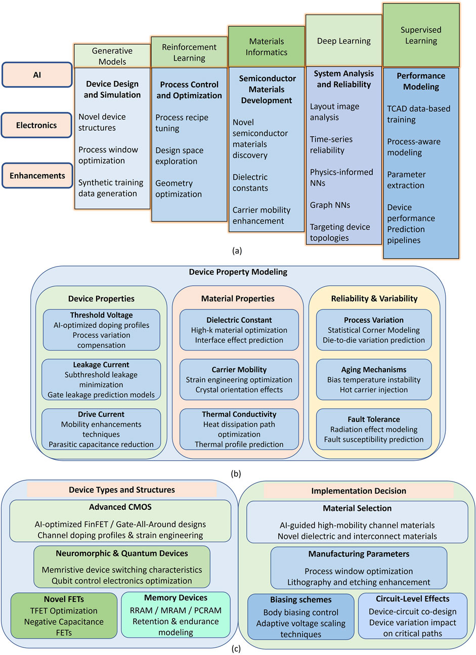
Figure 2. (a) AI techniques for semiconductor device engineering (b) Device properties influenced by AI in semiconductor chip design (c) Left Panel: device types and structures, Right Panel: implementation decision - layer on device and design decisions.
7 Future outlook
7.1 Use case applications in industry
AI has already made a substantial impact in nanoelectronics manufacturing, revolutionizing processes across design, production, testing, and logistics. Industry leaders have adopted AI technologies to enhance efficiency, reduce costs, and improve product quality. For example, Intel employs AI-driven predictive maintenance systems in its semiconductor fabrication plants. These systems analyze data from sensors embedded in manufacturing equipment to predict failures before they occur, minimizing downtime and maximizing production output. Similarly, TSMC uses AI algorithms to optimize photolithography and wafer inspection processes. In component manufacturing, Siemens has integrated AI-powered solutions in its factories through its MindSphere platform, which enables real-time monitoring and optimization of production lines. This platform leverages AI to analyze fabrication tool performance and make adjustments, improving throughput and reliability. Foxconn, one of the largest electronics manufacturers, uses AI-driven robots to automate assembly lines, especially for precision tasks such as component placement and soldering in smartphones and laptops. These robots operate with exceptional accuracy, enabling mass production while maintaining high-quality standards.
Cadence Design Systems and Synopsys provide AI-powered EDA tools that streamline PCB and chip layout optimization and error detection. These tools quickly analyze complex circuit designs and identify potential issues, drastically reducing design cycles and accelerating time-to-market. In testing and verification, Advantest, a leader in automated test equipment, uses AI to optimize test plans and improve defect coverage, resulting in faster validation of semiconductor devices. In logistics and inventory management, Samsung has adopted AI to predict demand patterns and optimize supply chain operations. AI models forecast material requirements and dynamically adjust supply routes to avoid disruptions, enabling just-in-time delivery and reducing excess inventory. Amazon Robotics, widely employed in electronics warehouses, uses AI-powered robots to automate sorting, packing, and shipping processes, enhancing efficiency and accuracy in distribution networks.
AI is also making an impact on sustainability in electronics manufacturing. IBM applies AI models to monitor energy usage and reduce carbon footprints in its production processes. Additionally, HP has implemented AI algorithms to improve material recycling by identifying and sorting reusable components, advancing efforts in sustainable manufacturing. As a leader in AI adoption, General Electric utilizes AI in digital twins of physical products and systems, to test performance and predict maintenance needs before manufacturing begins. This approach reduces waste, optimizes designs, and accelerates innovation. These real-world examples highlight the role of AI in reshaping electronics manufacturing by improving efficiency, enhancing quality, and promoting sustainability. As AI technologies continue to evolve, they are expected to drive even greater advancements across the industry, ensuring competitiveness and meeting growing demands for smarter and more sustainable electronic products.
7.2 Perspective
We are witnessing a significant shift in the design and delivery of the electronics that power our world. From smartphones to complex systems, electronics are increasingly integrated into our daily lives. Currently, the convergence of AI and nanotechnology is transforming the electronics supply chain, necessitating both technological advancements and a human-centered approach. As this convergence advances, five areas of foundational nanotechnology stand out: material discovery, device optimization, circuits and systems synthesis, chip testing and verification, and digital modeling through the use of twins. Each of these areas is undergoing change not merely due to the speed or power of AI, but because it is evolving into a more effective tool that supports decision-making, expands capabilities, and assists engineers in developing smarter, more sustainable technologies.
The discovery of new materials for electronics has traditionally involved a combination of scientific knowledge, practical experience, and intuition. The integration of AI is accelerating this process, not by replacing engineers, but by facilitating the exploration of possibilities that may otherwise be unfeasible to test manually. AI models predict how a new compound might behave or which material combinations could offer better performance or sustainability. It should be noted that AI cannot be trusted blindly; every model must be scrutinized, and every prediction validated. AI does not eliminate the need for human insight; rather, it prompts specific questions to be asked about the outputs it generates. In this process, AI acts as a co-pilot rather than a replacement.
As devices become smaller and more powerful, performance optimization becomes more complex. AI explores millions of possible design options, finding the best trade-offs between speed, power use, cost, and reliability. It is to be observed that understanding a design is not just a math problem, it involves goals and risk analysis, reiterating the need for AI systems to be explainable. Engineers need to understand the logic behind a suggested design, which helps teams make better, informed decisions ensuring that safety, sustainability, even fairness remain part of the process.
In the past, building a complex chip could take years. Now, AI helps automate parts of this process, especially at the level of circuits and entire systems. However, automation can sometimes be perceived as a black box; it is efficient, yet challenging to trust. A structured approach should maintain the involvement of engineers, utilizing AI to manage repetitive tasks while affording individuals the opportunity to adjust, investigate, and confirm designs. The integration of machines and humans in a collaborative framework leverages the scalability and speed of automation alongside human capabilities in judgment, context, and creativity. This synergy ensures that both entities contribute effectively to the operational process.
Testing and verifying chips represents one of the most critical and time-consuming stages in electronics manufacturing. AI can assist in identifying errors early, simulating real-world usage, and predicting failures before they occur. However, maintaining trust is crucial, as errors during this stage could lead to defective products or significant safety risks. Consequently, it is imperative that AI tools are designed to be transparent and auditable. Trustworthy AI is not merely a feature; it is a fundamental responsibility.
Digital twins, virtual replicas of physical systems, are becoming vital in electronics. They let engineers test ideas without building expensive prototypes, saving time and resources. AI helps make these models more accurate and useful, allowing for simulation of everything from nanoscale behaviors to system-wide interactions.
The changes seen today are similar to those of the early days of computers. During that time, the shift from analog to digital created entirely new industries, ways of working, and ways of thinking. Today, AI and nanotechnology are pushing those boundaries again, this time within the materials and systems that make emerging digital technologies. The opportunity is enormous, but it comes with responsibility. Design must consider not just efficiency, but also fairness; not just performance, but sustainability; and not just speed, but understanding.
At the edge of this new Frontier in nanoelectronics, AI is not a magic answer; it is a powerful tool. When guided by human values, it can help discover new materials, optimize devices, improve systems, ensure safety, and better model the world that is being built. Consequently, there is an urgent need to realign educational curricula to reflect this interdisciplinary reality. Students must be trained not only in AI algorithms or electronic design, but also in systems thinking and ethics. Lifelong learning opportunities should be made available to current professionals whose roles are evolving alongside these technologies. Outreach must not be an afterthought; it must be part of the central mission. The public must be engaged: not merely as consumers of advanced electronics, but as stakeholders whose trust, understanding, and perspectives shape the trajectory of technological adoption.
8 Conclusion
The integration of AI into electronics manufacturing is fundamentally reshaping material discovery, device design, fabrication processes, and system optimization. AI-driven methodologies enhance predictive modeling, process control, and defect detection, addressing critical challenges in scalability, variability, and resource efficiency. Machine learning and reinforcement learning algorithms enable real-time parameter tuning, optimizing fabrication precision while reducing defects and process drift. AI-accelerated simulations improve the design and validation of emerging materials and device architectures by refining multi-physics models and reducing computational overhead. Despite these advancements, several technical challenges remain. The accuracy and generalizability of AI models depend on the availability of high-fidelity datasets, which are often constrained by experimental limitations. Ensuring AI-driven solutions integrate effectively with existing manufacturing workflows requires robust data pipelines, interoperability frameworks, and standardized validation methodologies. Furthermore, AI-optimized circuit design and heterogeneous computing architectures must align with existing EDA toolchains to achieve practical scalability. Future research should focus on developing interpretable AI models that incorporate domain-specific physics constraints, enabling reliable extrapolation to novel materials and device configurations. Autonomous optimization frameworks, digital twin-based process control, and generative design approaches will be instrumental in reducing prototyping cycles and improving manufacturing adaptability. Establishing rigorous methodologies for uncertainty quantification in AI-driven predictions is critical for ensuring reliability across applications. Continued innovation in AI algorithms, coupled with improvements in experimental characterization techniques, will drive progress toward highly efficient, scalable, and adaptive manufacturing systems.
Data availability statement
The original contributions presented in the study are included in the article/supplementary material, further inquiries can be directed to the corresponding authors.
Author contributions
SS: Conceptualization, Data curation, Formal Analysis, Investigation, Methodology, Project administration, Resources, Software, Validation, Visualization, Writing – original draft, Writing – review and editing. TP: Conceptualization, Formal Analysis, Funding acquisition, Investigation, Methodology, Project administration, Resources, Supervision, Validation, Visualization, Writing – original draft, Writing – review and editing.
Funding
The author(s) declare that financial support was received for the research and/or publication of this article. We acknowledge support of the UKRI AI programme, the Engineering and Physical Sciences Research Council, for APRIL- EPSRC AI Hub for Productive Research and Innovation in electronics (grant number EP/Y029763/1) and Royal Academy of Engineering (RAEng) Chair in Emerging Technologies under Grant CiET1819/2/93.
Conflict of interest
The authors declare that the research was conducted in the absence of any commercial or financial relationships that could be construed as a potential conflict of interest.
Generative AI statement
The author(s) declare that no Generative AI was used in the creation of this manuscript.
Publisher’s note
All claims expressed in this article are solely those of the authors and do not necessarily represent those of their affiliated organizations, or those of the publisher, the editors and the reviewers. Any product that may be evaluated in this article, or claim that may be made by its manufacturer, is not guaranteed or endorsed by the publisher.
References
Ahmadi, M., Ziatdinov, M., Zhou, Y., Lass, E. A., and Kalinin, S. V. (2021). Machine learning for high-throughput experimental exploration of metal halide perovskites. Joule 5 (11), 2797–2822. doi:10.1016/j.joule.2021.10.001
Aleksandrov, P., Rezaei, A., Dutta, T., Xeni, N., Asenov, A., and Georgiev, V. (2023b). Convolutional machine learning method for accelerating nonequilibrium green’s function simulations in nanosheet transistor. IEEE Trans. Electron Devices 70 (10), 5448–5453. doi:10.1109/ted.2023.3306319
Aleksandrov, P., Rezaei, A., Xeni, N., Dutta, T., Asenov, A., and Georgiev, V. (2023a). “Fully convolutional generative machine learning method for accelerating non-equilibrium green’s function simulations,” in 2023 international conference on simulation of semiconductor processes and devices (SISPAD), 169–172.
Alexopoulos, K., Nikolakis, N., and George, C. (2020). Digital twin-driven supervised machine learning for the development of artificial intelligence applications in manufacturing. Int. J. Comput. Integr. Manuf. 33 (5), 429–439. doi:10.1080/0951192x.2020.1747642
Ardichvili, A. (2022). The impact of artificial intelligence on expertise development: implications for hrd. Adv. Dev. Hum. Resour. 24 (2), 78–98. doi:10.1177/15234223221077304
Arinez, J. F., Chang, Q., Gao, R. X., Xu, C., and Zhang, J. (2020). Artificial intelligence in advanced manufacturing: current status and future outlook. J. Manuf. Sci. Eng. 142 (11), 110804. doi:10.1115/1.4047855
Badini, S., Regondi, S., and Pugliese, R. (2023). Unleashing the power of artificial intelligence in materials design. Materials 16 (17), 5927. doi:10.3390/ma16175927
Basak Chowdhury, A., Tan, B., Garg, S., and Ramesh, K. (2022). Robust deep learning for ic test problems. IEEE Trans. Computer-Aided Des. Integr. Circuits Syst. 41 (1), 183–195. doi:10.1109/tcad.2021.3054808
Basu, A., Saha, A., Banerjee, S., Roy, P. C., and Kundu, B. (2024). A review of artificial intelligence methods in predicting thermophysical properties of nanofluids for heat transfer applications. Energies 17 (6), 1351. doi:10.3390/en17061351
Batra, R., Song, Le, and Ramprasad, R. (2021). Emerging materials intelligence ecosystems propelled by machine learning. Nat. Rev. Mater. 6 (8), 655–678. doi:10.1038/s41578-020-00255-y
Bennett, C., and Eder, K. (2025). Review of machine learning for micro-electronic design verification.
Bird, C., Ford, D., Zimmermann, T., Forsgren, N., Kalliamvakou, E., Lowdermilk, T., et al. (2023). Taking flight with copilot. Commun. ACM 66 (6), 56–62. doi:10.1145/3589996
Botifoll, M., Pinto-Huguet, I., and Arbiol, J. (2022). Machine learning in electron microscopy for advanced nanocharacterization: current developments, available tools and future outlook. Nanoscale Horizons 7 (12), 1427–1477. doi:10.1039/d2nh00377e
Butola, R., Li, Y., and Reddy Kola, S. (2022). A machine learning approach to modeling intrinsic parameter fluctuation of gate-all-around si nanosheet mosfets. IEEE Access 10, 71356–71369. doi:10.1109/access.2022.3188690
Cai, J., Chu, X., Xu, K., Li, H., and Wei, J. (2020). Machine learning-driven new material discovery. Nanoscale Adv. 2 (8), 3115–3130. doi:10.1039/d0na00388c
Carrion Schafer, B., and Wang, Zi (2019). High-level synthesis design space exploration: past, present, and future. IEEE Trans. Computer-Aided Des. Integr. Circuits Syst. 39 (10), 2628–2639. doi:10.1109/tcad.2019.2943570
Cauwenberghs, G., Cong, J., Sharon Hu, X., Joshi, S., Mitra, S., Porod, W., et al. (2023). Micro/nano circuits and systems design and design automation: challenges and opportunities [point of view]. Proc. IEEE 111 (6), 561–574. doi:10.1109/jproc.2023.3276941
Chau-Cheung Cheng, K., Chen, L. L.-Y., Li, J.-W., Li, K.S.-M., Tsai, N.C.-Y., Wang, S.-J., et al. (2021). Machine learning-based detection method for wafer test induced defects. IEEE Trans. Semicond. Manuf. 34 (2), 161–167. doi:10.1109/tsm.2021.3065405
Chaudhuri, A., Liu, C., Fan, X., and Chakrabarty, K. (2021). C-testing and efficient fault localization for ai accelerators. IEEE Trans. Computer-Aided Des. Integr. Circuits Syst. 41 (7), 2348–2361. doi:10.1109/tcad.2021.3107401
Chen, H., Liu, M., Tang, X., Zhu, K., Sun, N., and Pan, D. Z. (2020). Challenges and opportunities toward fully automated analog layout design. J. Semicond. 41 (11), 111407. doi:10.1088/1674-4926/41/11/111407
Chen, H., Zheng, Y., Li, J., Li, L., and Wang, X. (2023). Ai for nanomaterials development in clean energy and carbon capture, utilization and storage (ccus). ACS Nano 17 (11), 9763–9792. doi:10.1021/acsnano.3c01062
Chen, Mu Ku, Liu, X., Sun, Y., and Tsai, D. P. (2022). Artificial intelligence in meta-optics. Chem. Rev. 122 (19), 15356–15413. doi:10.1021/acs.chemrev.2c00012
Chen, Y.-L., Sacchi, S., Dey, B., Blanco, V., Halder, S., Leray, P., et al. (2024). Exploring machine learning for semiconductor process optimization: a systematic review. IEEE Trans. Artif. Intell. 5 (12), 5969–5989. doi:10.1109/tai.2024.3429479
Cheng, C.-K., Ho, C.-T., Holtz, C., and Lin, B. (2021). “Design and system technology co-optimization sensitivity prediction for vlsi technology development using machine learning,” in 2021 ACM/IEEE international workshop on system level interconnect prediction (SLIP), 8–15.
Chu, W., Ho, P. S., and Li, W. (2021). An adaptive machine learning method based on finite element analysis for ultra low-k chip package design. IEEE Trans. Components, Packag. Manuf. Technol. 11 (9), 1435–1441. doi:10.1109/tcpmt.2021.3102891
El-Sayed, S. A., Spyrou, T., Camuñas-Mesa, L. A., and Stratigopoulos, H.-G. (2022). Compact functional testing for neuromorphic computing circuits. IEEE Trans. Computer-Aided Des. Integr. Circuits Syst. 42 (7), 2391–2403. doi:10.1109/tcad.2022.3223843
Epps, R. W., Bowen, M. S., Volk, A. A., Abdel-Latif, K., Han, S., Reyes, K. G., et al. (2020). Artificial chemist: an autonomous quantum dot synthesis bot. Adv. Mater. 32 (30), 2001626. doi:10.1002/adma.202001626
Epps, R. W., Volk, A. A., Reyes, K. G., and Abolhasani, M. (2021). Accelerated ai development for autonomous materials synthesis in flow. Chem. Sci. 12 (17), 6025–6036. doi:10.1039/d0sc06463g
Fayazi, M., Colter, Z., Afshari, E., and Dreslinski, R. (2021). Applications of artificial intelligence on the modeling and optimization for analog and mixed-signal circuits: a review. IEEE Trans. Circuits Syst. I Regul. Pap. 68 (6), 2418–2431. doi:10.1109/tcsi.2021.3065332
Fayazi, M., Taba, M. T., Afshari, E., and Dreslinski, R. (2023). Angel: fully-automated analog circuit generator using a neural network assisted semi-supervised learning approach. IEEE Trans. Circuits Syst. I Regul. Pap. 70 (11), 4516–4529. doi:10.1109/tcsi.2023.3295737
Ferretti, L., Cini, A., Zacharopoulos, G., Alippi, C., and Pozzi, L. (2022). Graph neural networks for high-level synthesis design space exploration. ACM Trans. Des. Automation Electron. Syst. 28 (2), 1–20. doi:10.1145/3570925
Friederich, J., Francis, D. P., Lazarova-Molnar, S., and Mohamed, N. (2022). A framework for data-driven digital twins of smart manufacturing systems. Comput. Industry 136, 103586. doi:10.1016/j.compind.2021.103586
Fuhr, A. S., Ganesh, P., Vasudevan, R. K., Roccapriore, K. M., and Sumpter, B. G. (2024). Digital twins and deep learning segmentation of defects in monolayer mx2 phases. Appl. Phys. Lett. 124 (3), 2024. doi:10.1063/5.0181080
Furxhi, I., Lara, F., Zanoni, I., Brigliadori, A., Vespignani, M., and Costa, A. L. (2024). Design rules applied to silver nanoparticles synthesis: a practical example of machine learning application. Comput. Struct. Biotechnol. J. 25, 20–33. doi:10.1016/j.csbj.2024.02.010
Genssler, P. R., Barkam, H. E., Pandaram, K., Imani, M., and Amrouch, H. (2023). Modeling and predicting transistor aging under workload dependency using machine learning. IEEE Trans. Circuits Syst. I Regul. Pap. 70 (9), 3699–3711. doi:10.1109/tcsi.2023.3289325
Gholap, A. D., Uddin, Md J., Faiyazuddin, Md, Omri, A., Gowri, S., and Khalid, M. (2024). Advances in artificial intelligence for drug delivery and development: a comprehensive review. Comput. Biol. Med. 178, 108702. doi:10.1016/j.compbiomed.2024.108702
Gökgöz, B., Aydın, T., and Gül, F. (2024). Optimizing memristor-based synaptic devices for enhanced energy efficiency and accuracy in neuromorphic machine learning. IEEE Access 12, 154401–154417. doi:10.1109/access.2024.3482110
Gong, H., Cheng, S., Chen, Z., and Li, Q. (2022). Data-enabled physics-informed machine learning for reduced-order modeling digital twin: application to nuclear reactor physics. Nucl. Sci. Eng. 196 (6), 668–693. doi:10.1080/00295639.2021.2014752
Gulevich, D. G., Nabiev, I. R., and Samokhvalov, P. S. (2024). Machine learning–assisted colloidal synthesis: a review. Mater. Today Chem. 35, 101837. doi:10.1016/j.mtchem.2023.101837
Han, Yu, Tang, B., Wang, L., Bao, H., Lu, Y., Guan, C., et al. (2020). Machine-learning-driven synthesis of carbon dots with enhanced quantum yields. ACS Nano 14 (11), 14761–14768. doi:10.1021/acsnano.0c01899
Hei Chan, C., Sun, M., and Huang, B. (2022). Application of machine learning for advanced material prediction and design. EcoMat 4 (4), e12194. doi:10.1002/eom2.12194
Henman, P. (2020). Improving public services using artificial intelligence: possibilities, pitfalls, governance. Asia Pac. J. Public Adm. 42 (4), 209–221. doi:10.1080/23276665.2020.1816188
Heydari, S., Masoumi, N., Esmaeeli, E., Ayyoubzadeh, S. M., Ghorbani-Bidkorpeh, F., and Ahmadi, M. (2024). Artificial intelligence in nanotechnology for treatment of diseases. J. Drug Target. 32 (10), 1247–1266. doi:10.1080/1061186x.2024.2393417
Hirtz, T., Huurman, S., Tian, He, Yang, Yi, and Ren, T.-L. (2021). Framework for tcad augmented machine learning on multi-i–v characteristics using convolutional neural network and multiprocessing. J. Semicond. 42 (12), 124101. doi:10.1088/1674-4926/42/12/124101
Ho, Y.-W., Singh Rawat, T., Yang, Z.-K., Pratik, S., Lai, G.-W., Tu, Y.-L., et al. (2021). Neuroevolution-based efficient field effect transistor compact device models. IEEE Access 9, 159048–159058. doi:10.1109/access.2021.3130254
Hoang, A. T., Kennaway, M., Pham, D. T., Son Mai, T., Khalid, A., Rafferty, C., et al. (2024). “Deep learning enhanced side channel analysis on crystals-kyber,” in 2024 25th international symposium on quality electronic design (ISQED), 1–8.
Hong, G., Jeong, C., Huh, J. H. Y., Myung Choe, J., Kim, Y., and Jeong, C. (2025). Ml-driven compact models for rrams: addressing variability and simulation efficiency. IEEE Electron Device Lett. 46 (5), 876–879. doi:10.1109/led.2025.3545909
Humaid, Al N., Bahroun, Z., and Ahmed, V. (2024). Enhancing work productivity through generative artificial intelligence: a comprehensive literature review. Sustainability 16 (3), 1166. doi:10.3390/su16031166
Ibtesam, M., Saeed Solangi, U., Kim, J., Ansari, M. A., and Park, S. (2021). Highly efficient test architecture for low-power ai accelerators. IEEE Trans. Computer-Aided Des. Integr. Circuits Syst. 41 (8), 2728–2738. doi:10.1109/tcad.2021.3110739
Jain, S., and Narayanan, A. (2023). Digital twin–enabled machine learning for smart manufacturing. Smart Sustain. Manuf. Syst. 7 (1), 111–128. doi:10.1520/ssms20220035
Jeong, C., Myung, S., Huh, B. C., Kim, J., Jang, H., Lee, H., et al. (2021). Bridging tcad and ai: its application to semiconductor design. IEEE Trans. Electron Devices 68 (11), 5364–5371. doi:10.1109/ted.2021.3093844
Jiang, Y., Salley, D., Sharma, A., Keenan, G., Mullin, M., and Cronin, L. (2022). An artificial intelligence enabled chemical synthesis robot for exploration and optimization of nanomaterials. Sci. Adv. 8 (40), eabo2626. doi:10.1126/sciadv.abo2626
Jungmann, P., Johnson, J. B., Silva, E. C., Taylor, W., Khan, A. H., and Kumar, A. (2023). Tcad-enabled machine learning—an efficient framework to build highly accurate and reliable models for semiconductor technology development and fabrication. IEEE Trans. Semicond. Manuf. 36 (2), 268–278. doi:10.1109/tsm.2023.3240033
Kadulkar, S., Sherman, Z. M., Ganesan, V., and Truskett, T. M. (2022). Machine learning–assisted design of material properties. Annu. Rev. Chem. Biomol. Eng. 13, 235–254. doi:10.1146/annurev-chembioeng-092220-024340
Kim, I., Park, So J., Jeong, C., Shim, M., Kim, D. S., Kim, G.-T., et al. (2022). Simulator acceleration and inverse design of fin field-effect transistors using machine learning. Sci. Rep. 12 (1), 1140. doi:10.1038/s41598-022-05111-3
Kim, J., Kim, S. J., Han, J.-W., and Meyyappan, M. (2021b). Machine learning approach for prediction of point defect effect in finfet. IEEE Trans. Device Mater. Reliab. 21 (2), 252–257. doi:10.1109/tdmr.2021.3069720
Kim, M.-H., Hwang, S., Bang, S., Kim, T.-H., Lee, D. K., Hasan Raza Ansari, Md., et al. (2021a). A more hardware-oriented spiking neural network based on leading memory technology and its application with reinforcement learning. IEEE Trans. Electron Devices 68 (9), 4411–4417. doi:10.1109/ted.2021.3099769
Konstantopoulos, G., Koumoulos, E. P., and Charitidis, C. A. (2022). Digital innovation enabled nanomaterial manufacturing; machine learning strategies and green perspectives. Nanomaterials 12 (15), 2646. doi:10.3390/nano12152646
Kroll, J. A., Michael, J. B., and Thaw, D. B. (2021). Enhancing cybersecurity via artificial intelligence: risks, rewards, and frameworks. Computer 54 (6), 64–71. doi:10.1109/mc.2021.3055703
Kundu, S., Banerjee, S., Raha, A., Natarajan, S., and Basu, K. (2021). Toward functional safety of systolic array-based deep learning hardware accelerators. IEEE Trans. Very Large Scale Integration (VLSI) Syst. 29 (3), 485–498. doi:10.1109/tvlsi.2020.3048829
Kundu, S., Banerjee, S., Raha, A., Su, F., Natarajan, S., and Basu, K. (2023). Trouble-shooting at gan point: improving functional safety in deep learning accelerators. IEEE Trans. Comput. 72 (8), 2194–2208. doi:10.1109/tc.2023.3241218
Kwak, H., and Kim, J. (2023). Semiconductor multilayer nanometrology with machine learning. Nanomanufacturing Metrology 6 (1), 15. doi:10.1007/s41871-023-00193-7
Lai, Y., Yin, P., Yang, J., Ha, J., Deo, K. A., and Park, S. (2023). “Reflow oven zone temperature advisor using the ai-driven smart recipe generator,” in 2023 IEEE 73rd electronic components and technology conference (ECTC), 1773–1778.
Lampe, C., Kouroudis, I., Harth, M., Martin, S., Gagliardi, A., and Urban, A. S. (2023). Rapid data-efficient optimization of perovskite nanocrystal syntheses through machine learning algorithm fusion. Adv. Mater. 35 (16), 2208772. doi:10.1002/adma.202208772
Lau Neto, W., Li, Y., Gaillardon, P.-E., and Yu, C. (2022). Flowtune: end-to-end automatic logic optimization exploration via domain-specific multiarmed bandit. IEEE Trans. Computer-Aided Des. Integr. Circuits Syst. 42 (6), 1912–1925. doi:10.1109/tcad.2022.3213611
Li, J., Lim, K., Yang, H., Ren, Z., Raghavan, S., Chen, P.-Y., et al. (2020a). Ai applications through the whole life cycle of material discovery. Matter 3 (2), 393–432. doi:10.1016/j.matt.2020.06.011
Li, J., Tu, Y., Liu, R., Lu, Y., and Zhu, Xi (2020b). Toward “on-demand” materials synthesis and scientific discovery through intelligent robots. Adv. Sci. 7 (7), 1901957. doi:10.1002/advs.201901957
Li, X., Wu, Z., Rzepa, G., Karner, M., Xu, H., Wu, Z., et al. (2024). Overview of emerging semiconductor device model methodologies: from device physics to machine learning engines. Fundam. Res. doi:10.1016/j.fmre.2024.01.010
Lin, B.-S., Cheng, J.-S., Liao, H.-C., Yang, L.-Wu, Yang, T., and Chen, K.-C. (2021). Improvement of multi-lines bridge defect classification by hierarchical architecture in artificial intelligence automatic defect classification. IEEE Trans. Semicond. Manuf. 34 (3), 346–351. doi:10.1109/tsm.2021.3076808
Liu, B., Zhao, D., Lu, X., and Liu, Y. (2025). Process control in semiconductor manufacturing based on deep distributional soft actor-critic reinforcement learning. IEEE Trans. Semicond. Manuf. 38 (2), 210–231. doi:10.1109/tsm.2025.3539223
Liu, L., Bi, M., Wang, Y., Liu, J., Jiang, X., Xu, Z., et al. (2021). Artificial intelligence-powered microfluidics for nanomedicine and materials synthesis. Nanoscale 13 (46), 19352–19366. doi:10.1039/d1nr06195j
Lombardo, T., Duquesnoy, M., El-Bouysidy, H., Årén, F., Gallo-Bueno, A., Jørgensen, P. B., et al. (2021). Artificial intelligence applied to battery research: hype or reality? Chem. Rev. 122 (12), 10899–10969. doi:10.1021/acs.chemrev.1c00108
Maitra, V., Su, Y., and Shi, J. (2024). Virtual metrology in semiconductor manufacturing: current status and future prospects. Expert Syst. Appl. 249, 123559. doi:10.1016/j.eswa.2024.123559
Manley, M., Victor, A., Park, H., Kaul, A., Kathaperumal, M., and Bakir, M. S. (2024). Heterogeneous integration technologies for artificial intelligence applications. IEEE J. Explor. Solid-State Comput. Devices Circuits 10, 89–97. doi:10.1109/jxcdc.2024.3484958
Martins, R. M. F., and Lourenço, N. C. C. (2023). Analog integrated circuit routing techniques: an extensive review. IEEE Access 11, 35965–35983. doi:10.1109/access.2023.3265481
Mazhar Rathore, M., Shah, S. A., Shukla, D., Bentafat, E., and Bakiras, S. (2021). The role of ai, machine learning, and big data in digital twinning: a systematic literature review, challenges, and opportunities. IEEE Access 9, 32030–32052. doi:10.1109/access.2021.3060863
Mehta, K., Raju, S. S., Xiao, M., Wang, B., Zhang, Y., and Wong, H. Y. (2020). Improvement of tcad augmented machine learning using autoencoder for semiconductor variation identification and inverse design. IEEE Access 8, 143519–143529. doi:10.1109/access.2020.3014470
Mekki-Berrada, F., Ren, Z., Huang, T., Wong, W. K., Fang, Z., Xie, J., et al. (2021). Two-step machine learning enables optimized nanoparticle synthesis. npj Comput. Mater. 7 (1), 55. doi:10.1038/s41524-021-00520-w
Milo, V., Glukhov, A., Pérez, E., Zambelli, C., Lepri, N., Kalishettyhalli Mahadevaiah, M., et al. (2021). Accurate program/verify schemes of resistive switching memory (rram) for in-memory neural network circuits. IEEE Trans. Electron Devices 68 (8), 3832–3837. doi:10.1109/ted.2021.3089995
Noy, S., and Zhang, W. (2023). Experimental evidence on the productivity effects of generative artificial intelligence. Science 381 (6654), 187–192. doi:10.1126/science.adh2586
Oliveri, G., Salucci, M., and Massa, A. (2022). Towards efficient reflectarray digital twins-an em-driven machine learning perspective. IEEE Trans. Antennas Propag. 70 (7), 5078–5093. doi:10.1109/tap.2022.3155204
Osowiecki, W. T., Coogans, M. J., Sriraman, S., Ranjan, R., Lu, Yu J., and Fried, D. M. (2024). Achieving sustainability in the semiconductor industry: the impact of simulation and ai. IEEE Trans. Semicond. Manuf. 37 (4), 464–474. doi:10.1109/tsm.2024.3438622
Pan, J., Low, K.Lu, Ghosh, J., Jayavelu, S., Ferdaus, Md M., Lim, S.Yi, et al. (2021). Transfer learning-based artificial intelligence-integrated physical modeling to enable failure analysis for 3 nanometer and smaller silicon-based cmos transistors. ACS Appl. Nano Mater. 4 (7), 6903–6915. doi:10.1021/acsanm.1c00960
Pan, R., Bagherzadeh, M., Ghaleb, T. A., and Briand, L. (2022). Test case selection and prioritization using machine learning: a systematic literature review. Empir. Softw. Eng. 27 (2), 29. doi:10.1007/s10664-021-10066-6
Papadimitriou, I., Gialampoukidis, I., Vrochidis, S., and Kompatsiaris, I. (2024). Ai methods in materials design, discovery and manufacturing: a review. Comput. Mater. Sci. 235, 112793. doi:10.1016/j.commatsci.2024.112793
Park, J., Kim, Y. M., Hong, S., Han, B., Nam, Ki T., and Jung, Y. (2023). Closed-loop optimization of nanoparticle synthesis enabled by robotics and machine learning. Matter 6 (3), 677–690. doi:10.1016/j.matt.2023.01.018
Piccinotti, D., MacDonald, K. F., Gregory, S. A., Youngs, I., and Zheludev, N. I. (2020). Artificial intelligence for photonics and photonic materials. Rep. Prog. Phys. 84 (1), 012401. doi:10.1088/1361-6633/abb4c7
Pollice, R., Gomes, G. dos P., Aldeghi, M., Hickman, R. J., Krenn, M., Lavigne, C., et al. (2021). Data-driven strategies for accelerated materials design. Accounts Chem. Res. 54 (4), 849–860. doi:10.1021/acs.accounts.0c00785
Price, C. C., Li, Y., Zhou, G., Younas, R., Zeng, S. S., Scanlon, T. H., et al. (2024). Predicting and accelerating nanomaterial synthesis using machine learning featurization. Nano Lett. 24 (46), 14862–14867. doi:10.1021/acs.nanolett.4c04500
Qian, C., Liu, X., Ripley, C., Qian, M., Liang, F., and Yu, W. (2022). Digital twin—cyber replica of physical things: architecture, applications and future research directions. Future Internet 14 (2), 64. doi:10.3390/fi14020064
Qiao, Y., Chen, Y., Liu, F., Mei, Z., Luo, Y., Chen, Y., et al. (2025). Ra-unet: a new deep learning segmentation method for semiconductor wafer defect analysis on fine-grained scanning electron microscope (sem) images. IEEE Trans. Semicond. Manuf. 38 (2), 185–193. doi:10.1109/tsm.2025.3546296
Ren, J., Ahmad, R., Li, D., Ma, Y., and Hui, J. (2025). Industrial applications of digital twins: a systematic investigation based on bibliometric analysis. Adv. Eng. Inf. 65, 103264. doi:10.1016/j.aei.2025.103264
Ren, Z., Wan, J., and Deng, P. (2022). Machine-learning-driven digital twin for lifecycle management of complex equipment. IEEE Trans. Emerg. Top. Comput. 10 (1), 9–22. doi:10.1109/tetc.2022.3143346
Sadi, M., and Guin, U. (2021). Test and yield loss reduction of ai and deep learning accelerators. IEEE Trans. Computer-Aided Des. Integr. Circuits Syst. 41 (1), 104–115. doi:10.1109/tcad.2021.3051841
Scarabottolo, I., Ansaloni, G., Constantinides, G. A., Pozzi, L., and Reda, S. (2020). Approximate logic synthesis: a survey. Proc. IEEE 108 (12), 2195–2213. doi:10.1109/jproc.2020.3014430
Schlosser, T., Friedrich, M., Beuth, F., and Kowerko, D. (2022). Improving automated visual fault inspection for semiconductor manufacturing using a hybrid multistage system of deep neural networks. J. Intelligent Manuf. 33 (4), 1099–1123. doi:10.1007/s10845-021-01906-9
Senhora, F. V., Chi, H., Zhang, Y., Mirabella, L., Tang, T. L. E., and Paulino, G. H. (2022). Machine learning for topology optimization: physics-based learning through an independent training strategy. Comput. Methods Appl. Mech. Eng. 398, 115116. doi:10.1016/j.cma.2022.115116
Serov, N., and Vinogradov, V. (2022). Artificial intelligence to bring nanomedicine to life. Adv. Drug Deliv. Rev. 184, 114194. doi:10.1016/j.addr.2022.114194
Sheelvardhan, K., Guglani, S., Ehteshamuddin, M., Roy, S., and Dasgupta, A. (2023). Machine learning augmented compact modeling for simultaneous improvement in computational speed and accuracy. IEEE Trans. Electron Devices 71 (1), 239–245. doi:10.1109/ted.2023.3251296
Soldatov, M. A., Butova, V. V., Pashkov, D., Butakova, M. A., Medvedev, P. V., Chernov, A. V., et al. (2021). Self-driving laboratories for development of new functional materials and optimizing known reactions. Nanomaterials 11 (3), 619. doi:10.3390/nano11030619
Sundaram, S., and Zeid, A. (2023). Artificial intelligence-based smart quality inspection for manufacturing. Micromachines 14 (3), 570. doi:10.3390/mi14030570
Szymanski, N. J., Rendy, B., Fei, Y., Kumar, R. E., He, T., Milsted, D., et al. (2023). An autonomous laboratory for the accelerated synthesis of novel materials. Nature 624 (7990), 86–91. doi:10.1038/s41586-023-06734-w
Tan, P., Chen, X., Zhang, Hu, Wei, Q., and Luo, K. (2023). Artificial intelligence aids in development of nanomedicines for cancer management. Seminars Cancer Biol. 89, 61–75. doi:10.1016/j.semcancer.2023.01.005
Tao, H., Wu, T., Kheiri, S., Aldeghi, M., Aspuru-Guzik, A., and Kumacheva, E. (2021). Self-driving platform for metal nanoparticle synthesis: combining microfluidics and machine learning. Adv. Funct. Mater. 31 (51), 2106725. doi:10.1002/adfm.202106725
Tong, S., Jia, N., Luo, X., and Fang, Z. (2021). The janus face of artificial intelligence feedback: deployment versus disclosure effects on employee performance. Strategic Manag. J. 42 (9), 1600–1631. doi:10.1002/smj.3322
Traiola, M., Dos Santos, F. F., Rech, P., Cazzaniga, C., Sentieys, O., and Kritikakou, A. (2024). Impact of high-level-synthesis on reliability of artificial neural network hardware accelerators. IEEE Trans. Nucl. Sci. 71, 845–853. doi:10.1109/tns.2024.3377596
Venkataramani, S., Sun, X., Wang, N., Chen, C.-Yu, Choi, J., Kang, M., et al. (2020). Efficient ai system design with cross-layer approximate computing. Proc. IEEE 108 (12), 2232–2250. doi:10.1109/jproc.2020.3029453
Vikram, A., Brudnak, K., Zahid, A., Shim, M., and Kenis, P. J. A. (2021). Accelerated screening of colloidal nanocrystals using artificial neural network-assisted autonomous flow reactor technology. Nanoscale 13 (40), 17028–17039. doi:10.1039/d1nr05497j
Wang, Z., Li, L., Leon, R. C. C., Yang, J., Shi, J., van der Laan, T., et al. (2024). Improving semiconductor device modeling for electronic design automation by machine learning techniques. IEEE Trans. Electron Devices 71 (1), 263–271. doi:10.1109/ted.2023.3307051
Wang, Z., Li, L., and Yao, Y. (2021). A machine learning-assisted model for gan ohmic contacts regarding the fabrication processes. IEEE Trans. Electron Devices 68 (5), 2212–2219. doi:10.1109/ted.2021.3063213
Wang, Z., and Zhu, Xi (2024). Enhancing nanocrystal synthesis: a comparative study of online artificial intelligence optimization and offline high-throughput experimentation in chemical material discovery. ACS Appl. Nano Mater. 7 (6), 6499–6505. doi:10.1021/acsanm.4c00255
Weber, T., Brandmaier, M., Schmidt, A., and Mayer, S. (2024). Significant productivity gains through programming with large language models. Proc. ACM Human-Computer Interact. 8 (EICS)), 1–29. doi:10.1145/3661145
Wu, N., Li, Y., Yang, H., Chen, H., Dai, S., Hao, C., et al. (2024). Survey of machine learning for software-assisted hardware design verification: past, present, and prospect. ACM Trans. Des. Automation Electron. Syst. 29 (4), 1–42. doi:10.1145/3661308
Xia, K., Sacco, C., Kirkpatrick, M., Saidy, C., Nguyen, L., Kircaliali, A., et al. (2021). A digital twin to train deep reinforcement learning agent for smart manufacturing plants: environment, interfaces and intelligence. J. Manuf. Syst. 58, 210–230. doi:10.1016/j.jmsy.2020.06.012
Xiao, J., Ji, Q., Shen, Q., Jiang, J., Huang, Y., and Lou, J. (2022b). Accelerating stochastic-based reliability estimation for combinational circuits at rtl using gpu parallel computing. Int. J. Intelligent Syst. 37 (11), 8309–8326. doi:10.1002/int.22940
Xiao, Li, Zhan, Q., Sun, B., Feng, H., Zeng, Y., Wang, H., et al. (2022a). Scientific machine learning enables multiphysics digital twins of large-scale electronic chips. IEEE Trans. Microw. Theory Tech. 70 (12), 5305–5318. doi:10.1109/tmtt.2022.3208917
Xie, Y., Sattari, K., Zhang, C., and Lin, J. (2023a). Toward autonomous laboratories: convergence of artificial intelligence and experimental automation. Prog. Mater. Sci. 132, 101043. doi:10.1016/j.pmatsci.2022.101043
Xie, Z., Pan, J., Chang, C.-C., Hu, J., and Chen, Y. (2023b). The dark side: security and reliability concerns in machine learning for eda. IEEE Trans. Computer-Aided Des. Integr. Circuits Syst. 42 (4), 1171–1184. doi:10.1109/tcad.2022.3199172
Xu, C., Solomon, S. A., and Gao, W. (2023). Artificial intelligence-powered electronic skin. Nat. Mach. Intell. 5 (12), 1344–1355. doi:10.1038/s42256-023-00760-z
Xu, R. H. J., Keating, L. P., Vikram, A., Shim, M., and Kenis, P. J. A. (2024). Understanding hot injection quantum dot synthesis outcomes using automated high-throughput experiment platforms and machine learning. Chem. Mater. 36 (3), 1513–1525. doi:10.1021/acs.chemmater.3c02751
Xu, X., Aggarwal, D., and Shankar, K. (2022). Instantaneous property prediction and inverse design of plasmonic nanostructures using machine learning: current applications and future directions. Nanomaterials 12 (4), 633. doi:10.3390/nano12040633
Yang, R.Xi, McCandler, C. A., Andriuc, O., Siron, M., Woods-Robinson, R., Horton, M. K., et al. (2022). Big data in a nano world: a review on computational, data-driven design of nanomaterials structures, properties, and synthesis. ACS Nano 16 (12), 19873–19891. doi:10.1021/acsnano.2c08411
Zervakis, G., Amrouch, H., and Henkel, J. (2020). Design automation of approximate circuits with runtime reconfigurable accuracy. IEEE access 8, 53522–53538. doi:10.1109/access.2020.2981395
Zhang, P., Guo, Z., Ullah, S., Melagraki, G., Afantitis, A., and Lynch, I. (2021). Nanotechnology and artificial intelligence to enable sustainable and precision agriculture. Nat. Plants 7 (7), 864–876. doi:10.1038/s41477-021-00946-6
Zhao, S., Blaabjerg, F., and Wang, H. (2020). An overview of artificial intelligence applications for power electronics. IEEE Trans. Power Electron. 36 (4), 4633–4658. doi:10.1109/tpel.2020.3024914
Zhao, Z., and Zhang, L. (2020). An automated topology synthesis framework for analog integrated circuits. IEEE Trans. Computer-Aided Des. Integr. Circuits Syst. 39 (12), 4325–4337. doi:10.1109/tcad.2020.2977605
Keywords: artificial intelligence, nanoelectronics manufacturing, semiconductor design, nanotechnology applications, sustainable engineering, electronics supply chain
Citation: Sivasubramani S and Prodromakis T (2025) Reaching new frontiers in nanoelectronics through artificial intelligence. Front. Nanotechnol. 7:1627210. doi: 10.3389/fnano.2025.1627210
Received: 12 May 2025; Accepted: 10 June 2025;
Published: 25 June 2025.
Edited by:
Yi Xuan, University of Pittsburgh, United StatesReviewed by:
Soumyajit Mandal, Brookhaven National Laboratory (DOE), United StatesCopyright © 2025 Sivasubramani and Prodromakis. This is an open-access article distributed under the terms of the Creative Commons Attribution License (CC BY). The use, distribution or reproduction in other forums is permitted, provided the original author(s) and the copyright owner(s) are credited and that the original publication in this journal is cited, in accordance with accepted academic practice. No use, distribution or reproduction is permitted which does not comply with these terms.
*Correspondence: Santhosh Sivasubramani, c3NpdmFzdWJAZWQuYWMudWs=; Themis Prodromakis, dC5wcm9kcm9tYWtpc0BlZC5hYy51aw==