 Gabriel Maroli1
 Santiago Boyeras1Hernan Giannetta1Sebastian Pazos1
 Joel Gak2Alejandro Raúl Oliva3María Alicia Volpe4
 Pedro Marcelo Julian5Felix Palumbo1*
- 1UIDI-CONICET Universidad Tecnológica Nacional, Buenos Aires, Argentina
- 2Engineering Department, Universidad Católica del Uruguay, Montevideo, Uruguay
- 3DIEC- CONICET Universidad Nacional del Sur, Bahía Blanca, Argentina
- 4PLAPIQUI—CONICET Universidad Nacional del Sur, Bahía Blanca, Argentina
- 5Silicon Austria Labs GmbH, Science Park 4, Linz, Austria
Understanding the sintering process of conductive inks is a fundamental step in the development of sensors. The intrinsic properties (such as thermal conductivity, resistivity, thermal coefficient, among others) of the printed devices do not correspond to those of the bulk materials. In the field of biosensors porosity plays a predominant role, since it defines the difference between the geometric area of the working electrode and its electrochemical surface area. The analysis reported so far in the literature on the sintering of inks are based on their DC characterization. In this work, the shape and distribution of the nanoparticles that make up the silver ink have been studied employing a transmission electron microscopy. Images of the printed traces have been obtained through a scanning electron microscope at different sintering times, allowing to observe how the material decreases its porosity over time. These structural changes were supported through electrical measurements of the change in the trace impedance as a function of drying time. The resistivity and thermal coefficient of the printed tracks were analyzed and compared with the values of bulk silver. Finally, this work proposes an analytical circuit model of the drying behavior of the ink based on AC characterization at different frequencies. The characterization considers an initial time when the spheric nanoparticles are still surrounded by the capping agent until the conductive trace is obtained. This model can estimate the characteristics that the printed devices would have, whether they are used as biosensors (porous material) or as interconnections (compact material) in printed electronics.
1 Introduction
Printed electronics (PE) is a term that defines the printing of circuits not only on flexible substrates such as paper, textiles, Kapton, PEN and PET but also on a large number of potential media Neuvo and Ylönen (2009). PE merges electronics manufacturing and text/graphic printing. By this combination, one can manufacture high-quality electronic products which are thin, flexible, wearable, lightweight, of varying sizes, ultra-cost-effective, and environmentally friendly Suganuma (2014). Furthermore, in recent years, the printing of conductive metal nanoparticle inks such as silver and gold has not only shown its versatility in the manufacture of printed circuits but also its usefulness for the development of (bio) sensors and wearables Zub et al. (2022), Yang et al. (2022). A series of inks of different nature is necessary for inkjet printing. The most used conductive ink is based on silver Rama et al. (2015). This ink consists of a colloidal suspension of nanometer-sized silver particles with a thin stabilizer polymer coat. Because the nanoparticles (NPs) have a very high specific surface area, they are highly prone to sintering at a considerable low temperature (10%–20% of the melting point of the bulk material) Buffat and Borel (1976), Gao and Gu (2015), which is why the metal inks sinter at temperatures as low as 100°C–150°C Moon et al. (2005), temperatures much lower than silver melting point (962°C) Somiya and Moriyoshi (1990). After the ink has been printed on a substrate, it should be thermally cured. Thermal curing is a necessary step to establish electrical contact among nanoparticles. First, the evaporation of the solvent forms a continuous conductive thin film. Raising the temperature above that required for solvent evaporation initiates the polymer stabilizer elimination, allowing the stabilizer cover to move away from the interparticle regions, achieving metallic particles contact Greer and Street (2007). The sintering process is critical in the performance of the conductive trace, not only regarding to the electrical properties, but also to the mechanical ones Somiya and Moriyoshi (1990). Some authors have developed their own inks Rodriguez (2016); however, this is a trial and error process, where some physical parameters of the ink can be estimated prior to its manufacture. Understanding the sintering process of conductive inks is a fundamental step in developing sensors. The intrinsic properties (such as thermal conductivity, resistivity, thermal coefficient, among others) of the printed devices do not correspond to those of the bulk materials from which the nanoparticles have been obtained. This is mainly due to the fact that the material traces obtained have high porosity; in Trasatti and Petrii (1991), a percolative model that relates the resistivity of the inks with their porosity is presented. In the field of biosensors, porosity plays a predominant role since it defines the difference between the geometric area of the working electrode and its electrochemical surface area Zhao et al. (2016). The analysis reported so far in the literature on the sintering of inks is based on their DC characterization Greer and Street (2007). In this work, the shape and distribution of the nanoparticles that make up the silver ink have been studied employing a transmission electron microscopy (TEM). Images of the printed traces have been obtained through a scanning electron microscope (SEM) at different sintering times, allowing to observe how the material decreases its porosity over time; these structural changes were supported through electrical measurements of the change in the trace impedance as a function of drying time. As a case study, the resistive thermal coefficient of the printed tracks was analyzed and compared with the value of the thermal coefficient of bulk silver. Finally, this work proposes an analytical circuit model of the drying behavior of the ink based on AC characterization at different frequencies. The characterization considers an initial time when the spheric nanoparticles are still surrounded by the capping agent until the conductive trace is obtained. This model can provide an estimation of the characteristics that the printed devices would have, whether they are used as biosensors (porous material) or as interconnections (compact material) in printed electronics.
2 Experimental
2.1 Ink preparation
In order to obtain an ink with rheological properties compatible with inkjet printing, silver nanoparticles stabilized powder (AgNPs), with an average size of 100 nm, from NanoTop (China), milli-Q water, ethanol, and TritonMT X-100 from Sigma-Aldrich were used. First, 31.58 g of ethanol (96% purity and density 0.8 g/ml) were mixed with 27.62 g of milli-Q quality water in a beaker. 0.8 g of TritonMT X-100 was added to the mixture. The solution was stirred at 3,000 rpm with T 25 digital LR disperser, from IKA, while the silver nanoparticles were sequentially incorporated in three steps, 13.33 g every 5 min, to improve homogenization. The stirring was continued for 1 hour, and finally, the solution was sonicated with a Q55 sonicator with standard probe 4422 from Q-Sonicator. The ink preparation was carried out at room temperature, except for the sonication step which was in an ice bath. A homogeneous 40 wt% silver ink was obtained. The ink was tested by drop casting and an Epson TX-135 consumer printer was used to test its printability.
2.2 TLM structure formation
First, 400 μl of ink were deposited on a 25 mm × 25 mm glass substrate using a 100–1,000 μl DragonLab micropipette. Once deposited, the ink was spinned at 1,000 rpm for 30 s with an acceleration of 250 rpm/s. Then, the sample was baked in an ORL-DH oven for 1 h at 150°C. After that, a new layer of silver ink was deposited, repeating the previous process. This process was repeated four times, achieving a
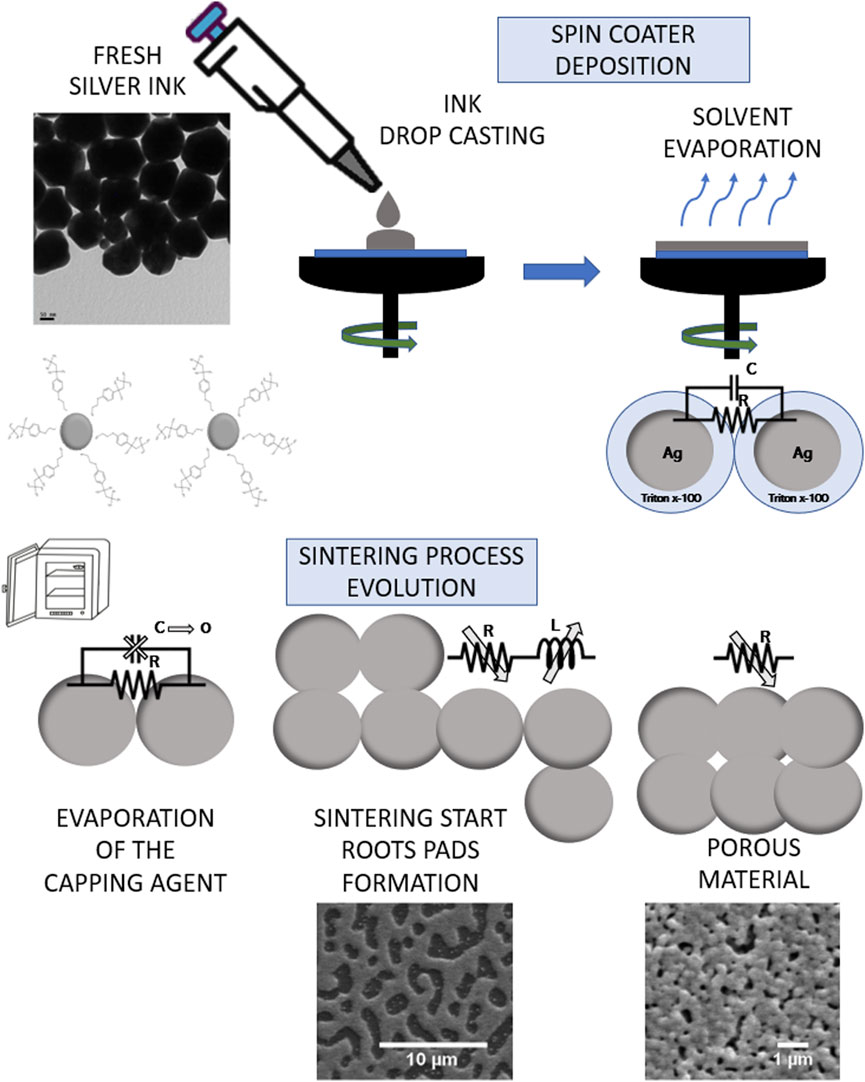
FIGURE 1. Schematic of the drying process, first the sample is placed in a spin coater, the solvent is evaporated at room temperature, and the Ag NPs are isolated from each other due to the capping agent (capacitive behavior). When heat is added, the sintering process begins with the elimination of the capping agent and the interconnection of the Ag NPs.
2.3 TEM and SEM images
An analysis of an ink drop was carried out using a TEM, Brand: JEOL, model 100 CX II, operated at an acceleration voltage of 100 kV and magnifications of 100000x and 270000x to determine the size of the nanoparticles (Supplementary Figure S2). Size measurements were performed with a Digital Micrograph software. The AgNPs size information is useful for estimating the initial capacitance of the ink, which is discussed in a subsequent section. In addition, the annealing process can be observed by means of a SEM throughout the drying time (Figures 1, 4). Supplementary Figure S2 shows that the ink has spherical nanoparticles of 100 nm average size. This information is essential in understanding the ink capacitance behavior at the beginning of drying. In the SEM images, shown in Figure 1, it can be seen that root-like paths are formed during drying. Subsequently, over time the ink turns into a continuous film.
2.4 Electrical characterization of the ink during sintering
The ink was characterized during the sintering process by impedance measurements performed at constant temperature inside the probe station, using an Agilent E4980A LCR meter and a triaxial thermal-chuck probe station. The samples were dried at 90°C and 120°C, contacted with metallic tips (as shown in Supplementary Figure S4 and the impedance was recorded as a function of time for frequencies from 10 kHz up to 1 MHz.
2.5 Electrical characterization of the sintered ink in DC
First, current-voltage (I-V) measurements were carried out on the different segments of the TLM structure. The purpose of these measurements was to determine the contact resistance as well as the resistivity of the ink. Measurements ranged from −40 to 100 mV with a current compliance of 100 mA. (I-V) measurements were carried out in the dark and at room temperature conditions, using a source measuring unit (SMU) Keithley 2636B. In order to determine the thermal coefficient of the ink, this measurement was repeated for different temperatures: 100, 125, 150, and 175°C (Supplementary Figure S3).
2.6 Results
Figure 2A shows the (I-V) results of the measurements carried out at room temperature. A linear relationship can be observed for the different segments of the TLM structure. This behavior is expected for the ink once the sintering process has been done since it becomes a resistive element. The measurements show a standard deviation of 0.55%. It can be seen that with the increase in the length of the segment, a smaller slope is obtained, and the resistance increases. The TLM measurement method relates the lengths with the increase in resistivity. The slope of the curve shown in Figure 2A presents units of Ω/mm, which corresponds to the linear resistance of the ink. The intercept is two times the contact resistance between the ink and the tip of the probe station. The slope is 2.5 Ω/mm, and the intercept is 0.17 Ω. Considering the geometric data of TLM structure designed Roberson et al. (2012), it can be concluded that the ink has a resistivity of 19.03 × 10⁻⁸ Ω.m, which is approximately 11.9 times larger than the bulk resistivity of silver. This value is consistent with that reported by different manufacturers for inks being dried at the same temperature SigmaAldrich (2020). As for the behavior of the ink as a function of temperature, it can be seen from Figure 2B that it is also linear; so, it could be modeled by R = R0(1 + αT). In this case, α = 7.8 × 10⁻³ Ω/°C, which is approximately twice as large as the silver bulk Reuss (2008). These changes in the intrinsic properties of the material can be explained by considering that sintered inks are porous materials. A percolative model of the sintered ink will be discussed in later sections since the material’s porosity is related to its electrochemical area.
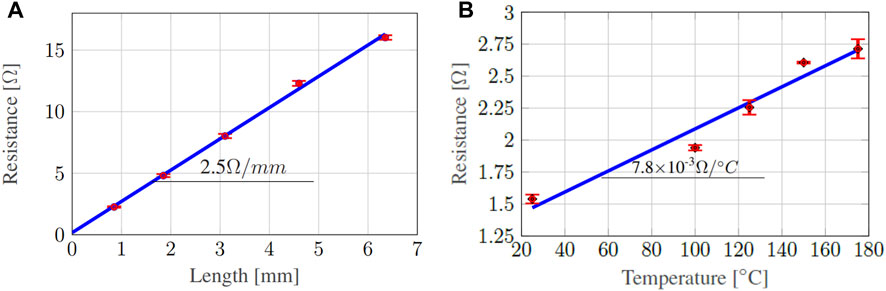
FIGURE 2. (A) Relationship between segment length and measured resistance. Graph obtained from the slopes of Supplementary Figure S4. The slope of the straight line that represents the linear resistivity of the trace is indicated. (B) Linear relationship between temperature and measured resistance. The slope of the straight line that represents the thermal coefficient of the trace is indicated.
3 Analysis
3.1 Analytic circuit model
The proposed model can predict the time and temperature the ink must be dried in order to reach a certain impedance. In addition, both the material’s porosity and the time needed for the ink to behave fully resistive could be determined. It is important to note that this is a handy tool for predicting the behavior and usefulness of a custom ink. Once the resistance has been determined, through the percolative model, it is possible to estimate the porosity and the electrochemical area that a given trace of silver will have, which is of great interest for sensors and biosensors. Based on the data obtained in the present work and the information collected from the works Greer and Street (2007) and Samano (2017), an analytic circuit model for ink drying as a function of time is proposed. Most works dealing with ink drying carry out measurements in DC, obtaining an exponential decrease in resistance. This phenomenon can be explained by the diffusive model proposed by Frenkel Frenkel (1945). In Samano (2017), the variation of the ink impedance is analyzed, both in module and phase, as a function of time for different frequencies. From the measurements made in AC, for temperatures of 90°C and 120°C, shown in Figure 3, and in accordance with the behavior observed in Samano (2017), a simplified circuit of a serial RL in parallel with a capacitor is proposed. According to this model,
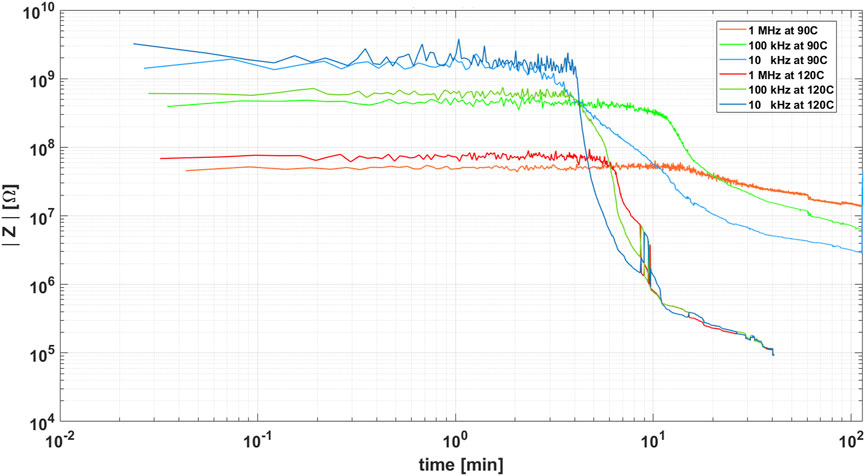
FIGURE 3. Comparison between drying at 120°C and 90°C, it is observed that the initial capacitances are the same, independent of the drying temperature. The temperature influences the sintering, and therefore the rate of change of impedance. Additionally, given that at 90°C the sintering speed is lower, the change in behavior of the ink from capacitive to inductive is observed.
Figure 3 shows that the fresh ink has a high impedance ranging from a few GΩ to tens of MΩ, depending on the frequency. From this information, it can be concluded that at the beginning of the drying, the ink is mainly capacitive, which agrees with the fact that before the heat treatment, the ink consists of small spheres very close to each other and coated by a dielectric. Before the sintering process starts, the capacitance of each sphere can be estimated as C = r/K Sears and Zemansky (2013), where r is the radius of the sphere, based on the size distribution of Supplementary Figure S2, with a value of 100 nm and K is the Coulomb constant (8.987 × 10⁹ Nm2/C2). Each AgNP has a capacitance of CNP = 1.11 × 10⁻¹⁷F. Figure 3 shows the experimental results corresponding to two samples that were sintered at different temperatures. It can be seen that the variation of impedance as a function of time is different, but the initial capacitance is the same, proving that the initial capacitance value is independent of the temperature at which the sintering is carried out. Given the geometry of the probe station tips, it is defined that the contact surface is 3.83 × 104 μm2, one-third of the tip area, and the distance between tips is 25 mm. Therefore, considering a layer thickness of 1 μm, a total initial capacitance can be estimated considering each NP as a nanocapacitor, placed in parallel with the contact tip and in series along the trace. The TEM image on the right top of Figure 1 shows that the NPs have a grouping behavior, that can be considered as if one were stuck to the other. Hence, the initial capacitance, C0, is given by:
This value is consistent with that obtained from the measurements in Figure 3, where it was calculated that the initial capacitance was 3.12 × 10⁻¹⁵F. This capacitance decreases as the dielectric that formerly coated the nanoparticles evaporates. Since the annealing is done at a temperature lower than the boiling point of the dielectric, the evaporation rate is proportional to the volatility of the substance, which is proportional to the vapor pressure. As shown in Figure 3, the slope of the impedance change depends on the drying temperature; therefore, a β value at 120°C has been experimentally determined. The following expression was obtained for the capacitance:
where β(120°C) = 0.02 1/min. From the analysis of the experimental impedance at the initial time for the different frequencies, an initial resistance R0 = 2.09 GΩ was determined, a value in line with previously reported ones (Rama et al., 2015). Based on the Greer model (Greer and Street., 2007), we know that the resistivity has two sintering models, so the following expression was obtained for the resistor:
where τ = 4.0 × 10⁸ s is the characteristic time for sintering by lattice diffusion Coble (1961), and γ(T)t = 0.2 1/min, as β, is an experimental adjustment parameter, which describes the rate of change of the resistance, therefore depending on the sintering temperature. The fresh ink does not have an inductive characteristic, so L (0, T) = 0. Likewise, the conductive tracks that give rise to inductance, are created at the same rate that the capacitive part disappears. For that reason, we have that:
Then, the traces begin to join at the same rate as the resistance decreases, resulting in a continuous film. The expression for the inductance is:
where td is a delay and L0 = 5 mH.
After replacing Eq. 3, Eq. 4 and Eq. 7 in Eq. 1, the model was simulated in Matlab®. Figure 4 shows the comparison between the model and the experimental results. After about 30 min, the system becomes fully resistive, and there is no longer a dependency on frequency.
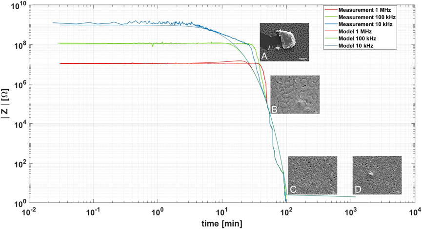
FIGURE 4. Superposition of the analytical model and the measurements made at three different frequencies [10 kHz (Blue), 100 kHz (Green) and 1 MHz (Red)], the capacitive behavior at the beginning of the measurement is observed and after 40 min the system becomes totally resistive. SEM images showing the evolution in the sintering of the ink are observed. (A–D) SEM images show the evolution of ink sintering over time.
3.2 Porosity determination
When developing a biosensor, it is essential to know the electrochemical area of the working electrode, which is possible to infer through the material’s porosity. The main application of this model is to determine the impedance that a printed trace will have through its physicochemical properties, the temperature and drying time. Furthermore, when the process of elimination of the capping agent and therefore capacitive behavior is completed, it is possible to infer the porosity of the material through the impedance value. Zhao et al. (2016) describes in his work an exponential model that relates the fraction of the voids in the sample with the resistance value; nevertheless, the proposed model is suitable for resistivities in the same order as the bulk silver resistivity. In the present work, to determine the fraction of the voids the SEM images obtained during the drying process were analyzed following the methodology described by Abdullah and Khairurrijal (2016). The fraction of the voids values obtained for the four SEM images in Figure 4 were 68%, 57%, 49% and 45%, respectively (Supplementary Figure S6). Equation 8 was proposed that fits for fraction of the voids of zero, i.e., a solid silver resistance, up to very high impedance values when the void fraction is up to 70%.
where Re(Z) is the real part of the impedance of the sintered ink, R0 is the resistance value of a pure silver resistor of the same dimensions, m = 0.3 is the exponential fit coefficient and fv is fraction of the voids. Supplementary Figure S7 shows a fit with an R2 = 0.9985.
4 Conclusion
In this paper it was shown that it is feasible to use commercial nanoparticles and of-the-shelf chemicals to generate the aqueous suspension for developing a custom ink. As it was shown by the physical and electrical characterization, the developed ink has properties that are comparable to those of commercial inks. This has great value due to the low price of nanoparticles in relation to a commercial ink. It was also shown that a straightforward circuit can model the ink’s drying with great fidelity. It was shown that capacitive and inductive behaviors can be observed throughout the drying process, not only in agreement with the experimental measurements and the data reported in the literature, but also in correlation with the physics of drying. It is important to highlight that knowing the physical parameters of the ink, such as the size of the nanoparticle, its surface energy, the diffusivity, the nature of the dielectric that coats the nanoparticle, its volatility, and the volatility of the solvent, allowed us to simulate the drying behavior that the ink would present at different temperatures. A compact model for the sintering process is helpful to characterize the quality of the ink and optimize the sintering step. In this way, we were able to determine if the substrate and the process were compatible with these parameters. Finally, it was shown how this analytical circuit model, in combination with a percolative model can be a valuable tool for the determination of the porosity of the material.
Data availability statement
The raw data supporting the conclusion of this article will be made available by the authors, without undue reservation.
Author contributions
GM contributed to the acquisition and analysis of the data as well as wrote the manuscript and led the project throughout. SB contributed to the acquisition and analysis of the data. HG contributed to the fabrication of the samples. SP contributed to the analysis of the data. JG, AO, MV, and PJ contributed to drafting the paper. FP conceived the original idea and supervised the project.
Funding
This work received funding from the following institutions: UTN.BA under projects CCUTIBA5219TC, CCUTIBA4764TC, CCUTNBA0005182, MATUNBA4936, and CONICET under projects PIP11220130100077CO and MINCyT under projects PICT2016/0579 and PICT 2017/2526. GM would like to express his gratitude to the Carolina Foundation for the financial support through the scholarship “Doctorado 2020”.
Acknowledgments
Special thanks to Ing. Maria Julia Yañez of the electron microscopy laboratory of the CONICET Bahía Blanca Scientific Center (CCTBB). To Ing. Juan José Ortiz and Lic. Fabián De Vita of the Argentine Nanotechnology Foundation. Lastly, to PLAPIQUI-CONICET-UNS and the UTN-FRBA Department of Chemical Engineering that have provided their facilities for this development.
Conflict of interest
The authors declare that the research was conducted in the absence of any commercial or financial relationships that could be construed as a potential conflict of interest.
Publisher’s note
All claims expressed in this article are solely those of the authors and do not necessarily represent those of their affiliated organizations, or those of the publisher, the editors and the reviewers. Any product that may be evaluated in this article, or claim that may be made by its manufacturer, is not guaranteed or endorsed by the publisher.
Supplementary material
The Supplementary Material for this article can be found online at: https://www.frontiersin.org/articles/10.3389/felec.2022.1060197/full#supplementary-material
References
Abdullah, M., and Khairurrijal, K. (2016). A simple method for determining surface porosity based on SEM images using OriginPro software. Indonesian J. Phys. 20, 37–40. doi:10.5614/itb.ijp.2009.20.2.4
Buffat, P., and Borel, J.-P. (1976). Size effect on the melting temperature of gold particles. Phys. Rev. A 13, 2287–2298. doi:10.1103/physreva.13.2287
Coble, R. (1961). Sintering crystalline solids. I. Intermediate and final state diffusion models. Appl. Phys. 32, 787. doi:10.1063/1.1736107
Frenkel, J. (1945). Viscous flow of crystalline bodies under the action of surface tension. Phys. 9, 385.
Gao, F., and Gu, Z. (2015). Handbook of nanoparticles, melting temperature of metallic nanoparticles. New York, United States: Springer, 661–690.
Greer, J. R., and Street, R. A. (2007). Thermal cure effects on electrical performance of nanoparticle silver inks. Acta Mater. 55, 6345–6349. doi:10.1016/j.actamat.2007.07.040
Moon, K. S., Dong, H., Maric, R., Pothukuchi, S., Hunt, A., Li, Y., et al. (2005). Thermal behavior of silver nanoparticles for low-temperature interconnect applications. Electron. Mater. 34, 168–175. doi:10.1007/s11664-005-0229-8
Neuvo, Y., and Ylönen, S. (2009). Bit bang rays to the future. Helsinki, Finland: Helsinki University Print.
Rama, V., Korada, V., Ps, K., and Singh, S. (2015). Conductive silver inks and its applications in printed and flexible electronics. London, United Kingdom: Royal Society of Chemistry, 1–60.
Reeves, G. K., and Harrison, H. B. (1982). Obtaining the specific contact resistance from transmission line model measurements. IEE Electron Device Lett. 3, 111–113. doi:10.1109/edl.1982.25502
Roberson, D., Wicker, R., and Macdonald, E. (2012). Ohmic curing of printed silver conductive traces. Electron. Mater. 41, 2553–2566. doi:10.1007/s11664-012-2140-4
Rodriguez, B. M. (2016). Inkjet and screen printing for electronic applications. Spain: Universitat de Barcelona.
Samano, A. (2017). “Measurements of conductive film,” Ph.D. thesis. (London: Brunel University London).
Sears, F., and Zemansky, M. (2013). University physics with modern physics technology. London, United Kingdom: Pearson.
SigmaAldrich (2020). Prepared for PFAS testing. Available at: https://www.sigmaaldrich.com/.
Somiya, S., and Moriyoshi, Y. (1990). Sintering key papers. Amsterdam, Netherlands: Elsevier Applied Science.
Trasatti, S., and Petrii, O. A. (1991). International union of pure and applied chemistry physical chemistry division commission on electrochemistry: Real surface area measurements in electrochemistry. Pure Appl. Chem. 63, 711–734. doi:10.1351/pac199163050711
Vinod, P. N. (2011). Specific contact resistance measurements of the screen-printed Ag thick film contacts in the silicon solar cells by three-point probe methodology and TLM method. Mater Sci. Mater Electron 22, 1248–1257. doi:10.1007/s10854-011-0295-z
Yang, Q., Rosati, G., Abarintos, V., Aroca, M. A., Osma, J. F., and Merkoçi, A. (2022). Wearable and fully printed microfluidic nanosensor for sweat rate, conductivity, and copper detection with healthcare applications. Biosens. Bioelectron. 202, 114005. doi:10.1016/j.bios.2022.114005
Zhao, Z., Mamidanna, A., Lefky, C., Hildreth, O., and Alford, T. L. (2016). A percolative approach to investigate electromigration failure in printed Ag structures. J. Appl. Phys. 120, 125104. doi:10.1063/1.4963755
Keywords: printed electronics, silver ink, sintering, wearables, analytical model
Citation: Maroli G, Boyeras S, Giannetta H, Pazos S, Gak J, Oliva AR, Volpe MA, Julian PM and Palumbo F (2023) Analytic circuit model for thermal drying behavior of electronic inks. Front. Electron. 3:1060197. doi: 10.3389/felec.2022.1060197
Received: 02 October 2022; Accepted: 13 December 2022;
Published: 06 January 2023.
Edited by:
Soumendu Sinha, Central Electronics Engineering Research Institute (CSIR), IndiaReviewed by:
Parasuraman Swaminathan, Indian Institute of Technology Madras, IndiaAbhijeet Sangle, Indian Institute of Technology Bombay, India
James Feng, Optomec, United States
Copyright © 2023 Maroli, Boyeras, Giannetta, Pazos, Gak, Oliva, Volpe, Julian and Palumbo. This is an open-access article distributed under the terms of the Creative Commons Attribution License (CC BY). The use, distribution or reproduction in other forums is permitted, provided the original author(s) and the copyright owner(s) are credited and that the original publication in this journal is cited, in accordance with accepted academic practice. No use, distribution or reproduction is permitted which does not comply with these terms.
*Correspondence: Felix Palumbo, RmVsaXgucGFsdW1ib0Bjb25pY2V0Lmdvdi5hcg==