 Navnidhi K. Upadhyay1,2*
 Thomas Blum2Petro Maksymovych2
 Nickolay V. Lavrik2Noraica Davila3Jordan A. Katine3A. V. Ievlev2
 Miaofang Chi2Qiangfei Xia1J. Joshua Yang1,4*
- 1Department of Electrical and Computer Engineering, University of Massachusetts, Amherst, MA, United States
- 2Oak Ridge National Laboratory, Center for Nanophase Materials Sciences, Oak Ridge, TN, United States
- 3Western Digital, San Jose, CA, United States
- 4Department of Electrical and Computer Engineering, University of Southern California, Los Angeles, CA, United States
Memristor devices have been extensively studied as one of the most promising technologies for next-generation non-volatile memory. However, for the memristor devices to have a real technological impact, they must be densely packed in a large crossbar array (CBA) exceeding Gigabytes in size. Devising a selector device that is CMOS compatible, 3D stackable, and has a high non-linearity (NL) and great endurance is a crucial enabling ingredient to reach this goal. Tunneling based selectors are very promising in these aspects, but the mediocre NL value limits their applications in large passive crossbar arrays. In this work, we demonstrated a trilayer tunneling selector based on the Ge/Pt/TaN1+x/Ta2O5/TaN1+x/Pd layers that could achieve a NL of 3 × 10⁵, which is the highest NL achieved using a tunnel selector so far. The record-high tunneling NL is partially attributed to the bottom electrode's ultra-smoothness (BE) induced by a Ge/Pt layer. We further demonstrated the feasibility of 1S1R (1-selector 1-resistor) integration by vertically integrating a Pd/Ta2O5/Ru based memristor on top of the proposed selector.
Introduction
Originally CBA was proposed and adapted for telecommunication switching systems at the beginning of the twentieth century (Craft, 1925). A relay switch was placed at each crosspoint to automatically and efficiently route any permutation of its n input (e.g., rows) to its m output lines (e.g., column; Scudder and Reynolds, 1939). Given the CBA architecture's simplicity and extremely high-density capability, it has recently been adapted for memory applications (Kuekes et al., 2000; Kuekes and Williams, 2001; Chen et al., 2003). A memristor (also called ReRAM, resistive random access memory, when used for memory) has a simple two-terminal structure, which is highly desirable for CBA implementation (Xia and Yang, 2019). CBA makes it possible to achieve a device footprint of 4F2. An even higher memory density (4F2/n; n: number of the stacked-layer) is achievable by 3D stacking the memristor devices (Lin et al., 2020). In light of these advantages, memristor-based CBA has emerged as one of the most promising technologies for high-density storage (Baek et al., 2005; Lee et al., 2009; Liu et al., 2014; Sills et al., 2014; Hudec et al., 2016) as well as memory-centric computing (Mouttet, 2008; Upadhyay et al., 2016, 2019; Rao et al., 2019; Lin et al., 2020; Wang et al., 2020). Memristor based CBAs can be used for solving linear regression, logistic regression, linear equations, matrix eigenvectors, differential equations, neural networks, etc. in one computing cycle in principle, in-situ within the CBA by using physical law such as Ohm's law for multiplication and Kirchhoff's law for summation (Rao et al., 2019; Sun et al., 2019, 2020; Wang et al., 2020). CBAs enable a time-saving and energy-efficient approach to solving a wide range of practical problems in the era of big data nowadays.
On the other hand, a CBA suffers from the so-called sneak path current issue (Yang et al., 2013; Xia and Yang, 2019). Sneak path current could be suppressed if we can somehow make the current-voltage relation of the “ON” state of memristor non-linear (Joshua Yang et al., 2012). This could be achieved in two ways: (1) By engineering intrinsic NL into the memristor device (Xie et al., 2006; Choi et al., 2011; Joshua Yang et al., 2012), or (2) Introducing a non-linear device, so-called selector, in series with the memristor (Upadhyay et al., 2020) at each crosspoint. In the first approach combining the non-linear mechanism and switching characteristics in one structure makes it difficult to optimize both the memory and selector performance simultaneously and independently. So far, the maximum non-linearity demonstrated by such devices falls well short of the required NL for large array implementations. Connecting a selector in series with a memristor (the 2nd approach) gives freedom of optimizing memristor and selector independently. A transistor can also be used as a select element in the so-called 1T1R (1-transistor 1-ReRAM) array (Rao et al., 2019; Wang et al., 2020). However, the 3-terminal structure and large footprint of transistors are not ideal for CBAs. The high processing temperature of the transistors makes it almost impossible to be used in 3D stacked memories. So the best approach to solve the sneak path problem is to use two-terminal thin-film-based selector devices that can be scaled laterally and stacked vertically together with a memristor (Chen, 2015; Burr et al., 2016).
In Supplementary Figure 1, we presented a table (extension of the table from Xia and Yang, 2019) comparing the figure of merits of all types of selector devices proposed in the literature. The tunneling selector stands out as the most promising one because of the following reasons: (1) electroforming-free operation; (2) low cycle to cycle variation; (3) high endurance (theoretically infinite); (4) in-principle low-temperature dependence; and (5) high-speed operation. In one of our recent work, we have demonstrated that such a tunneling selector even withstands the memristor's electroforming operation in a vertically integrated 1S1R cell (Upadhyay et al., 2020). This paper proposes a trilayer tunneling selector with a stack structure of Ge/Pt/TaN1+x/Ta2O5/TaN1+x/Pd. Here TaN1+x/Ta2O5/TaN1+x layers form the trilayer tunneling barrier structure. Ge/Pt and Pt layers are BE and top electrode (TE), respectively. We engineer the Ge/Pt BE to provide an ultrasmooth surface on which a trilayer stack could be deposited. The root-mean-square (rms) roughness and peak-to-valley height distribution of the Ge/Pt layer were measured to be 185 and 700 pm, respectively.
The requirements of a smooth BE surface for the tunneling selector will be discussed in detail in the next section. Using the proposed trilayer tunneling device, we have shown a record NL of 3 × 10⁵ and 107 for one-half and one-third biasing schemes, respectively. This is the highest NL among all tunneling based selectors reported so far. Furthermore, we integrated Pd/Ta2O5/Ru based memristor on top of the proposed selector device to realize a 1S1R cell. The 1S1R cell shows a maximum ON/OFF ratio of 100 and a NL of 104 and 106 for one-half and one-third biasing schemes, respectively. Again this is the highest NL demonstrated so far in any vertically integrated 1S1R cells to the best of our knowledge. The entire stack of the proposed 1S1R cell was deposited at room temperature, making it CMOS compatible and 3D stackable.
Tunneling Selector Design
Even though tunneling selectors have many advantages over other types of selectors, their mediocre value of NL has been a shortcoming. The highest NL reported in tunneling selectors was 1.1 × 10⁴, which we demonstrated in our previously reported work (Choi et al., 2016). We showed a trilayer tunneling barrier (TLTB) based selector could outperform the uniform barrier based selectors. As shown in Figure 1A, in the case of a uniform barrier device, the highest part of the barrier, closest to the electron source, is barely affected by the applied voltage. While for a “crested” barrier (Figure 1B) structure, the highest part of the barrier is in the middle and can be pulled down by the electric field quickly. Hence not only the barrier width but also the barrier height of such a crested barrier are much more sensitive to the applied electric field, resulting in a steeper current increase upon applied voltage and a higher non-linearity (Likharev, 1998; Jung and Cho, 2008). In other words, an applied voltage across the device only changes the barrier's width in the case of the regular rectangular barrier with a uniform barrier height. In contrast, both the barrier's width and height are reduced simultaneously upon applied voltages for the crested barrier. In practice, we can approximate a crested barrier structure with the staircase potential patterns formed in a trilayer structure, as shown in Figure 1C. We can achieve such a staircase energy barrier structure by sandwiching a dielectric layer with a small electron affinity between two other dielectric layers with larger electron affinities. This structure could be exploited for designing a high non-linearity selector. In this paper, we present a trilayer tunneling selector based on Ge/Pt/TaN1+x/Ta2O5/TaN1+x/Pd layers. The proposed TLTB (TaN1+x/Ta2O5/TaN1+x) layers form a staircase-like energy band structure, as shown in Supplementary Figure 2. This has been discussed in detail in our previous paper (Choi et al., 2016).
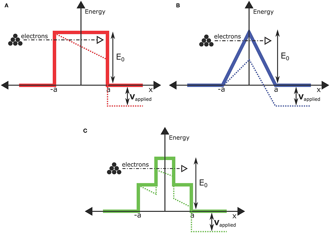
Figure 1. Band diagrams of different tunnel barriers. (A) Typical uniform potential barrier; (B) triangular symmetric potential barrier; (C) staircase symmetric potential barrier.
For designing a robust tunneling selector device, one needs to take care of two critical factors: (1) Depositing a high-quality dielectric layer that has minimal defects (e.g., Oxygen vacancies) and is stoichiometric and dense, which could be achieved by optimizing the deposition (sputtering in our case) recipe for the dielectric layers; (2) Having smooth surfaces and interfaces that can sustain a high electric field without breakdown. The roughness in the device stack could create hot spots due to the electric field concentration effect, resulting in an increase of the leakage current at relatively low voltage and low NL. With an increasing voltage, these hot spots can quickly cause a breakdown of the thin tunneling layers at relatively low voltages. To verify this hypothesis, we performed surface engineering for the device BE to obtain a much-smoothened surface. We found that depositing Pt on a thin Ge nucleation layer helps to achieve a smooth BE. For a comparative study, we deposited (evaporated) Ta (2 nm)/Pt (15 nm), Ti (2 nm)/Pt (15 nm), and Ge (2 nm)/Pt (15 nm) layers on a Si/SiO2 substrate. Figure 2 shows atomic force microscopy (AFM) topographic images of different surfaces. Figure 2A shows the rms (root mean square) roughness (Rq) of the substrate (Si/SiO2) surface, which was measured to be 0.116 nm. Figures 2B,C present topographic images of the commonly used BE stacks Ta/Pt and Ti/Pt, with the Rq being 0.306 and 0.314 nm, respectively. Figure 2D presents the value of Rq for the Ge/Pt layer, which came out to be 0.185 nm. To ascertain uncertainties in the rms roughness measurement, we have done additional analysis presented in Supplementary Figure 3. The Ge/Pt layer not only has a significantly lower Rq but also a narrower peak-to-valley surface topological height distribution compared to those of Ta/Pt and Ti/Pt films, as shown in Supplementary Figure 4. The reason why a Ge nucleation layer provides smooth Pt film may be related to the activation energy of diffusion. If the activation energy of Pt diffusion on Ge is higher than those on the Ta and Ti surfaces, in that case, it could reduce the surface diffusion and mass transportation of Pt on the Ge nucleation layer, which could result in a smoother surface topology (Logeeswaran et al., 2009). Ge/Pt layer also provides good adhesion with the substrate but maybe not as great as Ti/Pt and Ta/Pt layers.
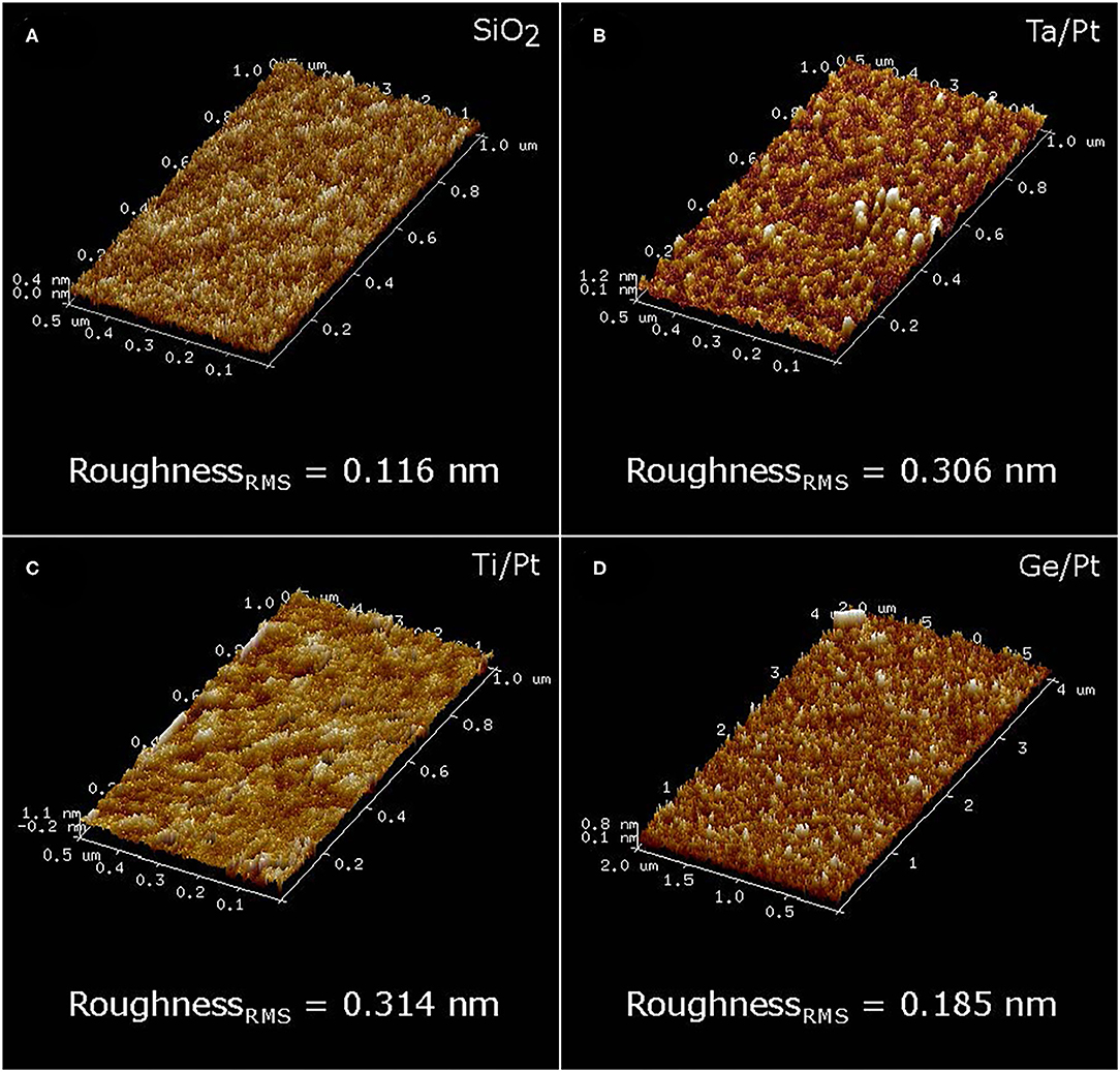
Figure 2. Atomic force microscopy (AFM) topographic images of different surfaces. (A) SiO2 (Substrate) surface. (B) Ta/Pt. (C) Ti/Pt. (D) Ge/Pt.
Next, we propose and demonstrate a highly non-linear TLTB selector device built upon the engineered smooth BE layers, as schematically shown in Figure 3A. Given that the BE smoothness is very critical to improving the performance of the TLTB selector device and the BE roughness will be affected by the surface roughness of the substrate itself, we took extensive measures to make sure the polished Si/SiO2 (100 nm) substrate surface is clean and smooth. Starting with dipping the substrate in the Piranha solution [a mixture of H2SO4: H2O2 (3:1)] for 10 min, so residual organics were removed from the sample surface, followed by rinsing in the deionized water, followed by a blow-dry using compressed N2 gun. Then to further smoothen out the substrate surface, CHF3 + O2 plasma cleaning (Turner and Chi, 2003; Ashraf et al., 2017) was performed in a Reactive Ion Etching (RIE) chamber for 2 min. Finally, the substrate was cleaned with acetone in the ultrasonic bath for 10 min to remove any particle/contamination from the previous plasma cleaning step. We then rinsed it in IPA (Isopropanol) in the ultrasonic bath for 10 min to dissolve the acetone with the contaminant, followed by a blow-dry using compressed N2. Immediately after finishing the substrate cleaning procedure, a photoresist (PR) was spin-coated on the substrate to maintain the surface cleanliness for the subsequent deposition of selector layers.
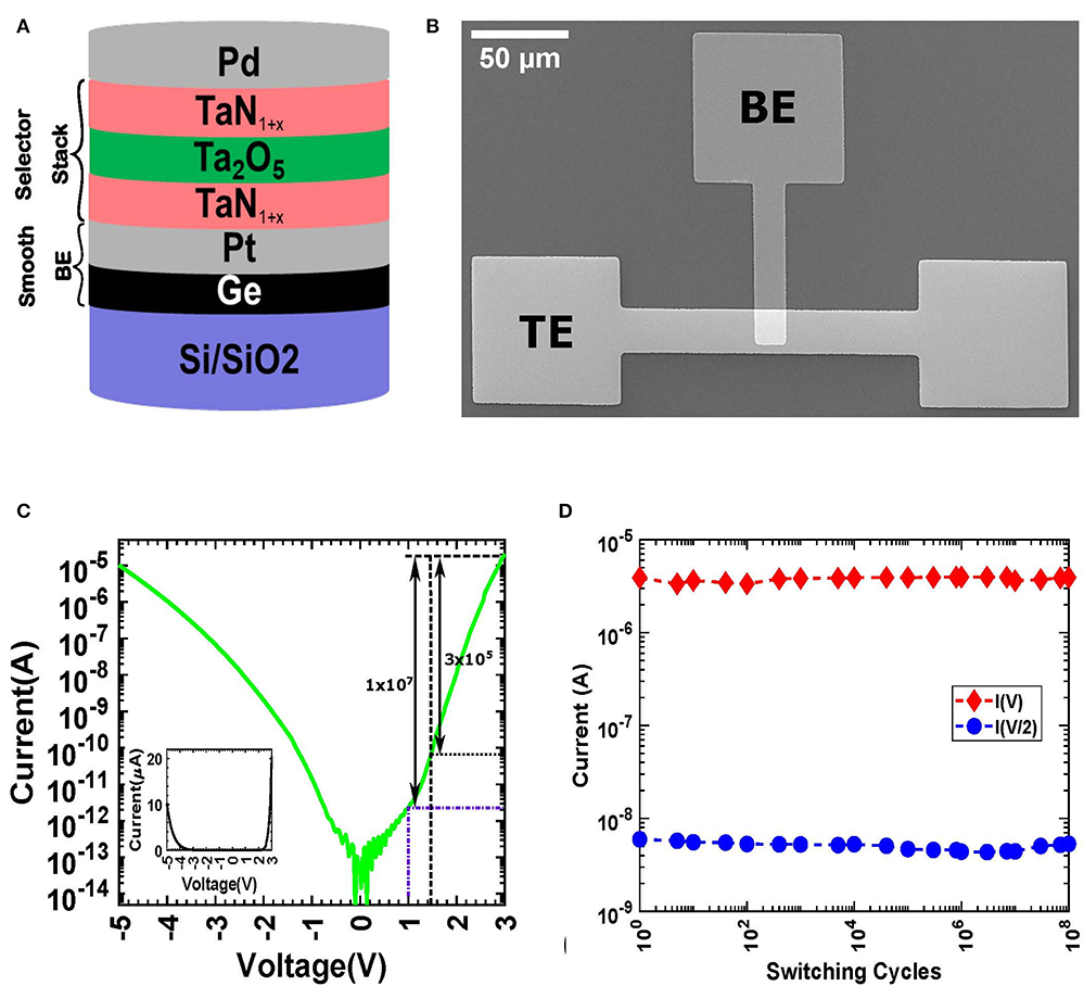
Figure 3. Trilayer tunneling selector device performance. (A) Schematic of the proposed selector device. (B) Scanning electron microscopy image showing a top-view image of the fabricated device. (C) A typical non-linear I–V curve of the selector device. The inset shows a linear plot of the I–V curve. (D) Endurance data measured up to 100 million cycles.
The PR coated substrate was then exposed by UV (ultraviolet) light through a mask for defining BE, then Ge (2 nm)/Pt (15 nm) layer was deposited using the e-beam evaporator followed by the standard lift-off process. Tri-layer tunneling stack [TaN1+x (4 nm)/Ta2O5 (3 nm)/TaN1+x (4 nm)] was deposited as a blanket layer without breaking the vacuum, using RF magnetron sputtering. The TaN1+x layers were deposited using a ceramic TaN (99.99%) target in Ar + N2 medium. The TaN target has a 1:1 ratio of Ta & N, which gives it metallic characteristics. Using Ar + N2 mixture as the deposition gas medium, the deposited TaN1+x film's conductivity could be tuned based on the N2 partial pressure (Yu et al., 2002). Similarly, an Ar + O2 medium was used for Ta2O5 deposition using a ceramic Ta2O5 (99.99%) target. The presence of a low oxygen partial pressure during the sputtering improves the density and the stoichiometry of the sputtered Tantalum oxide film (Duggan et al., 1993). Finally, the standard photolithography process was used to define the TE, and Pd (40 nm) was deposited using DC sputtering, followed by the lift-off process. It is worth noting that the entire selector stack was deposited at room temperature, making this proposed device CMOS compatible. The SEM (scanning electron microscope) micrograph of the 20 μm × 15 μm crosspoint device is presented in Figure 3B.
Keysight B1500 device parameter analyzer was used to measure the I–V characteristics of the selector device. Bias was applied to the TE, and the BE was grounded. The I–V characteristics of the proposed TLTB selector device is plotted (semi-log) in Figure 3C, where the inset shows the linear plot of the same sweep cycles. The proposed TLTB selector device shows very insulating behavior under low bias (≈70 pA at +1.5 V). It becomes highly conductive at a high bias (≈20.4 μA at +3 V), which results in a highly non-linear I–V characteristic of the proposed selector device. For one-half-voltage scheme NL is defined as NL1/2 = I(Vread)/I(Vread/2) and for one-third biasing scheme NL could be given as NL1/3 = I(Vread)/I(Vread/3). The measured NL of the device is around 3 × 10⁵ (107) for one-half (one-third biasing) schemes, as indicated in Figure 3C, which is the highest NL of any tunneling selector device reported so far. Supplementary Figure 5 shows multiple I–V sweep of the selector device. A control sample with the same TLTB structure but on different BE layers, i.e., Ti/Pt, showed a NL of about 100, as shown in Supplementary Figure 6, which indicates the importance of using a smooth BE for tunneling selector devices. Endurance measurement was conducted on the proposed selector device for 100 Million cycles without any noticeable degradation, as shown in Figure 3D, using 5 μs wide 3 V (Vread) and 1.5 V (Vread/2) pulses. It should be noted here that we used B1530A Waveform Generator/Fast Measurement Unit (WGFMU) for the endurance measurement. The noise floor of WGFMU unit is limited to a few nA of current, which resulted in a smaller NL (Compare to the actual NL of the selector device), observed during the endurance test.
To further demonstrate the effect of the proposed smooth BE (Ge/Pt) on tunneling selectors, we fabricated uniform barrier devices consisting of the TLTB stack's layers. Supplementary Figure 7 shows the schematic of the devices and their electrical performance. Supplementary Figures 7A,B shows schematic of the Ge/Pt/Ta2O5/Pd and Ge/Pt/TaN1+x/Pd devices and Supplementary Figures 7C,D shows their respective I–V characteristics. The NL of the single tunnel barrier selectors based on Ta2O5 and TaN1+x layers was measured to be 2 × 10³ and 1 × 10³, respectively. It is worth noting that the NL demonstrated by these simple uniform barrier devices is an order of magnitude higher than the NL of previously reported similar single barrier devices and other tunneling selector devices (Kawahara et al., 2013; Woo et al., 2014). We attribute this improvement in NL to the use of a Ge/Pt based smooth BE layer.
Vertically Integrated 1S1R Cell
To demonstrate the feasibility of integrating the proposed selector device with a memristor, a vertically integrated 1S1R cell has been fabricated. We used a recently proposed Ru based memristor device (Yoon et al., 2020) for this demonstration. Ru based memristor exhibit forming free and low power switching operations, making it suitable for a 1S1R integration. Figure 4A presents a schematic of the vertically integrated 1S1R stack. A polished Si/SiO2 (100 nm) substrate was cleaned and Ge (2 nm)/Pt (15 nm), TaN1+x (4 nm)/Ta2O5 (3 nm)/TaN1+x (4 nm) layers were deposited following the methods described in the previous section. Afterward, the Middle electrode (ME) was patterned using photolithography. A 40 nm thick Pd layer as the ME was sputter-deposited on top of the tri-layer tunneling stack, followed by the lift-off process. To isolate the selector layer from the memristor layer to be deposited on top of it, a 20 nm thick SiO2 blanket isolation layer was deposited using sputtering. Then the SiO2 isolation layer was patterned and etched away using the RIE (CHF3 + O2) to define the device region (see Supplementary Figure 8 for details). A 10 nm thick blanket Ta2O5 switching layer was deposited using RF magnetron sputtering. Finally, the TE was patterned using the photolithography process, and a 40 nm thick Ru layer was sputter-deposited using the DC magnetron sputtering followed by the lift-off process (see the Experimental Section for more details). Supplementary Figure 8 presents a wide-angle view of the cross-section of the 1S1R device. For the top memristor (1R) device, the Ru (TE) acts as an active electrode, while Pd (ME) serves as the inert electrode. It is worth noting that in this vertically integrated 1S1R cell, the selector was deliberately placed at the bottom to exploit the smooth BE (Ge/Pt) for achieving a high NL. We designed this testing structure in a way that the ME can be electrically accessed so that measurements can be made not only on the “1S1R” cell but also on the individual “S” and “R” to better understand the device stack.
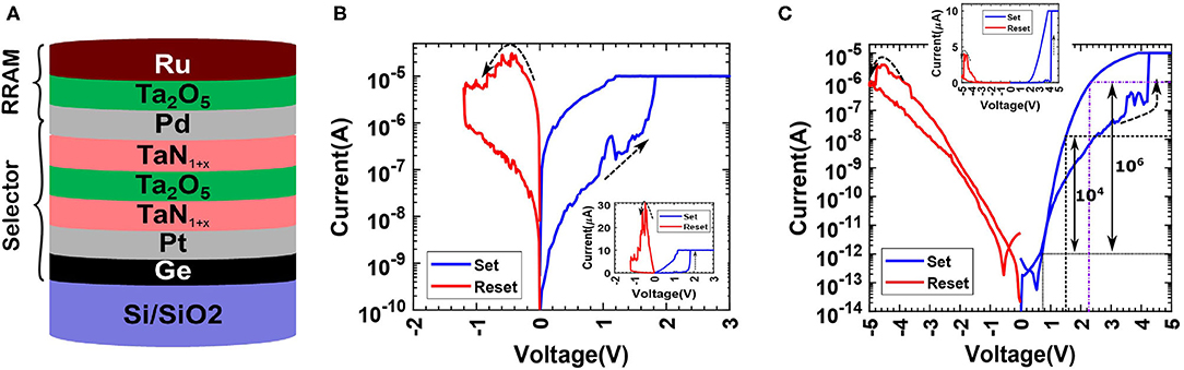
Figure 4. Vertically integrated 1S1R cell. (A) Schematic of the 1S1R cell. (B) Typical I–V characteristics of the Pd/Ta2O5/Ru based memristor device. (C) Typical I–V characteristics of the 1S1R cell with highly non-linear ON state. The inset shows a linear plot of the same I–V.
For characterizing the Ru based memristor device, bias was applied to the TE of the integrated cell, the ME was grounded, and the BE was left floating. Figure 4B presents the I–V characteristics of the memristor device. To SET the device, a positive dual-sweep voltage (blue lines) was applied with current compliance (Icc) set to 10 μA. Starting with a high resistance state (HRS), the device switched to a low resistance state (LRS) at 1.8 V and maintained its state during the reverse sweep. A negative dual-sweep voltage (red lines) was applied to RESET the device without any Icc. Beginning with the LRS, device RESET started at about −0.4 V, and it switched to HRS at about −1.2 V and maintained its state afterward during the reverse sweep. The linear plot of the same I–V is presented in the inset. This switching mechanism is attributable to the Ru conductive path's formation/rupture in the switching layer. A metallic path in the LRS is corroborated also by the Ohmic behavior observed in the LRS (Yoon et al., 2020).
Next, the vertically integrated 1S1R cell was electrically tested to demonstrate successful 1S-1R operations. Bias was applied to the TE, and the BE was grounded with the ME left floating. The non-linear I–V characteristic of the device is presented in Figure 4C. The 1S1R cell exhibit a NL of 104 (106) for one-half (one-third) biasing scheme at Vread = 1.5 V with an ON/OFF ratio of around 50. The highest ON/OFF ratio of 100 could be achieved at Vread = 3.4 V but with a reduced NL value of 150. Interestingly there is a trade-off between high NL and maximum memory window size and can be leveraged depending on the use cases. It should be noted that adding a resistor (memristor in the 1S1R) reduces the NL of the selector by an amount depending on the relative resistance of the resistor and the selector. Nevertheless, the non-linearity exhibited in the proposed 1S1R cell is the highest among any vertically integrated 1S1R cell presented so far to the best of our knowledge. SEM micrograph showing the vertically integrated 1S1R device's top view is presented in Figure 5a. TE, ME, and BE are marked on the figure. Cross-section scanning transmission electron microscopy (STEM) image of the 1S1R cell (Ge/Pt/TaN1+x/Ta2O5/TaN1+x/Pd/Ta2O5/Ru) is presented in Figure 5b. STEM micrograph revealed that the TLTB layers were amorphous. Time-of-Flight Secondary Ion Mass Spectrometry (ToF-SIMS) was conducted at the active region of the 1S1R device. Figure 5c presents the depth profile through the vertically integrated 1S1R cell, identifying the stack's key elements.
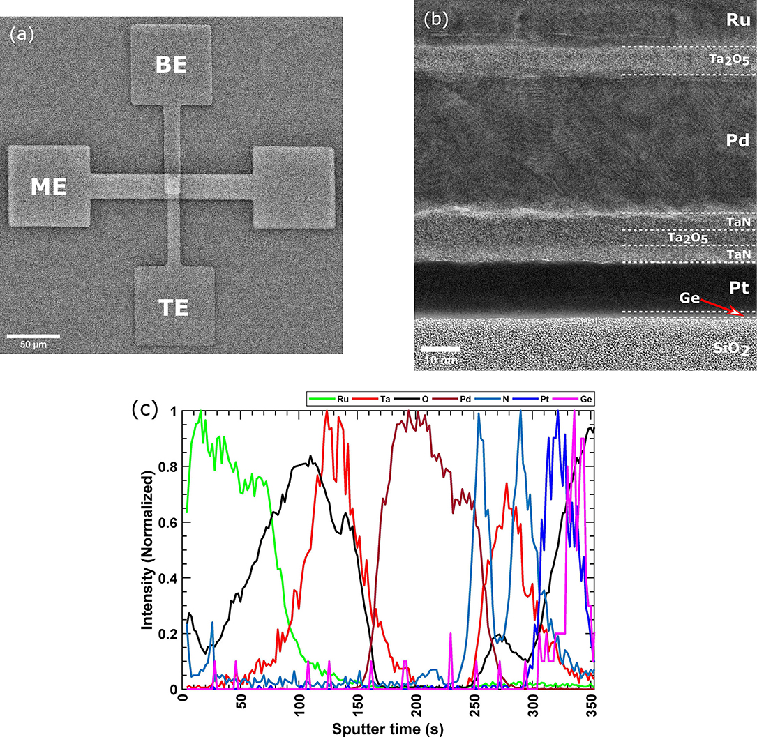
Figure 5. Physical characterization of the vertically integrated 1S1R cell. (a) Scanning electron microscopy image of the 1S1R cell showing the top view of the device. (b) Cross-sectional STEM image of the 1S1R cell. (c) ToF-SIMS depth profile through the layers of the vertically integrated 1S1R cell.
To demonstrate the proposed selector capability, we did a circuit simulation of the 1S1R based CBA. The SPICE model was validated by comparing the experimental and simulated I–V characteristics of the single device, as shown in Figure 6A. The normalized readout margin for different sizes of the CBA is presented in Figure 6B. We considered the two most popular biasing schemes for our simulation: one-half and one-third voltage schemes. The readout margin for a 100 kbits CBA is around 20% for the one-half biasing scheme and more than 90% for the one-third biasing scheme. The one-third biasing scheme is more resilient to the sneak path current issue than the one-half biasing scheme. We can conclude from the results that the proposed selector helps mitigate the effect of the CBA's sneak path currents. It could potentially support a larger array size before the read margin hits the minimum criterion of 10% to differentiate the states (Lo et al., 2013). Supplementary Figure 9 presents the readout resistance state of the selected device for various array sizes. HRS resistance decreases with array size because of an increase in sneak path current. Since readout current for LRS is larger than HRS, LRS current is only mildly affected by the sneak path current and so does the LRS resistance state.
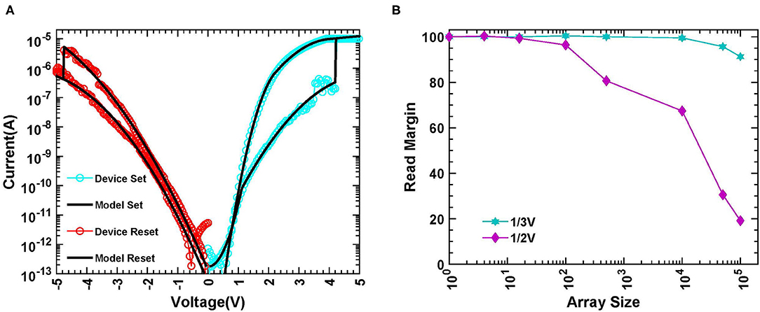
Figure 6. Circuit level modeling of 1S1R based CBA. (A) SPICE simulation of single device IV sweep (solid line), (B) Normalize Readout Margin for different array sizes.
Conclusion
In summary, we proposed and experimentally verified the critical role of layer smoothness and tunnel barrier shape in determining tunnel-based selectors' non-linearity. To prove the concepts, we developed a Ge/Pt/TaN1+x/Ta2O5/TaN1+x/Pd based TLTB selector, which combined the benefit of a staircase potential barrier with the smooth BE. The proposed selector is CMOS compatible, 3D stackable, and exhibits a record NL value. We have engineered the BE layer (Ge/Pt) to make it an ultrasmooth surface. The measured rms roughness and peak-to-valley height distribution were 185 and 700 pm, respectively. This ultrasmooth BE surface and crested barrier lead to the demonstration of a record-high NL of 3 × 10⁵. We further vertically integrated the proposed TLTB selector with a Ru based (Pd/Ta2O5/Ru) memristor device to demonstrate the feasibility of 1S1R integration and operation. The I–V characteristics recorded from this vertically integrated 1S1R cell show a maximum ON/OFF ratio of 100 and a NL of 104, also a record-high NL of any vertically integrated 1S1R cell ever reported. The excellent device NL performance suggests that our selector could be used to realize a large passive memristor array, which has remained elusive so far.
Experimental Section
Trilayer Selector Fabrication
A p-type (100) Si wafer with 100 nm thermal oxide was used as the substrate. The standard photolithography and lift-off process were used to define 15 μm wide Ge (2 nm)/Pt (15 nm) bottom electrode and 20 μm wide Pt (20 nm) top electrode using e-beam evaporation. A trilayer structure consists of TaN1+x (4 nm)/Ta2O5 (3 nm)/TaN1+x (4 nm) layers were sputter-deposited on top of the BE without breaking vacuum. TaN & Ta2O5 ceramic targets were used for RF magnetron sputtering in an Orion 8 (AJA international) sputtering system in the presence of an Ar-N2 mixture (15:5) and Ar-O2 mixture (20:1), respectively. Finally, 15 μm wide Pd (40 nm) was sputter-deposited following standard photolithography and lift-off process.
Vertically Integrated 1S1R Device Fabrication
On a p-type (100) Silicon substrate with 100 nm thick thermal oxide, a 20 μm wide Ge (2 nm)/Pt (15 nm) line (BE) defined by photolithography and lift-off process, was fabricated. Then a trilayer structure consists of TaN1+x (4 nm)/Ta2O5 (3 nm)/TaN1+x (4 nm) layers were sputter-deposited on top of the BE without breaking vacuum. TaN & Ta2O5 ceramic targets were used for RF magnetron sputtering in an Orion 8 (AJA international) sputtering system in the presence of Ar-N2 mixture and Ar-O2 mixture, respectively. Afterward, a 15 μm wide middle electrode was patterned by photolithography, and a 40 nm thick Pd layer was deposited by RF magnetron sputtering followed by a lift-off process. A 20 nm thick SiO2 isolation layer was sputter deposited on the top of the selector layer to isolate it (in the non-device-region) from the memristor layers to be deposited on top of it. The SiO2 layer in the device region was patterned and etched away before a 10 nm thick blanket Ta2O5 switching layer was deposited using RF magnetron sputtering. Finally, 10 μm wide TE was patterned using photolithography, and then a Ru (40 nm) layer was deposited using sputtering followed by a lift-off process.
Device Characterization
The DC measurements were performed using a B1500A semiconductor parameter analyzer (Keysight), and B1530A (Keysight) was used for pulse measurement. All electrical measurements were performed by applying the bias to the TE and grounding the BE. The cross-sectional TEM study of the Ge/Pt/TaN1+x/Ta2O5/TaN1+x/Pd/Ta2O5/Ru device and the EDS element mapping was performed using JEOL NEOARM atomic-resolution STEM at an accelerating voltage of 200 kV. FEI Nova 200 Dual-Beam FIB was used to prepare the FIBed TEM lamella. ToF-SIMS measurements were done using a TOF.SIMS.5-NSC instrument, using a Bi3+ ion gun (30 keV energy, 0.49 nA current) as the primary ion source and an O2− ion gun (1 keV energy, 120 nA current, 20 μm spot size) as the sputter source. ToF-SIMS measurements were performed in the non-interlaced mode, where every scan of chemical analysis with primary bismuth source was followed by sputtering using an O2− ion gun. A low energy electron flood gun was used for charge compensation between cycles. The vacuum level in the ToF-SIMS during the measurements ranged from 5 to 9 × 10⁻⁹ mbar.
SPICE Modeling
The device model was written using Verilog-A. Cadence Virtuoso was used for the circuit simulation. For all the simulations worst-case scenario has been considered. The selected device lies farthest to the row voltage source as well as farthest to the column current sense amplifier. All the unselected and half selected devices were switched to ON state before start of simulation.
Data Availability Statement
The original contributions presented in the study are included in the article/Supplementary Material, further inquiries can be directed to the corresponding author/s.
Author Contributions
JY conceived the concept. JY, QX, and NU designed the experiments, fabricated the devices, and performed electrical measurements. MC, NU, and TB carried out the STEM experiments. AI and NU performed the TOF-SIMS experiments. PM, NL, ND, and JK helped with experiments and data analysis. JY and NU wrote the paper. All authors discussed the results and implications and commented on the manuscript.
Funding
Part of this research was conducted at the Center for Nanophase Materials Sciences, which is a DOE Office of Science User Facility. This work was also partially supported by Air Force Office of Scientific Research (AFOSR) for the support through the MURI program under Contract No. FA9550-19-1-0213 and the U.S. Air Force Research Laboratory (AFRL) (Grant No. FA8750-18-2-0122). This work was also partially supported by the National Science Foundation under contract No. 2023752. Any opinions, findings and conclusions, or recommendations expressed in this material are those of the authors and do not necessarily reflect the views of AFRL.
Conflict of Interest
The authors declare that the research was conducted in the absence of any commercial or financial relationships that could be construed as a potential conflict of interest.
Supplementary Material
The Supplementary Material for this article can be found online at: https://www.frontiersin.org/articles/10.3389/fnano.2021.656026/full#supplementary-material
References
Ashraf, M., Sundararajan, S. V., and Grenci, G. (2017). Low-power, low-pressure reactive-ion etching process for silicon etching with vertical and smooth walls for mechanobiology application. J. Micro Nanolithogr. MEMS MOEMS 16:034501. doi: 10.1117/1.jmm.16.3.034501
Baek, I. G., Kim, D. C., Lee, M. J., Kim, H.-J., Yim, E. K., Lee, J. E., et al. (2005). “Multi-layer cross-point binary oxide resistive memory (OxRRAM) for post-NAND storage application,” in IEEE InternationalElectron Devices Meeting, 2005. IEDM Technical Digest (Washington, DC), 750–753. doi: 10.1109/IEDM.2005.1609462
Burr, G. W., Shenoy, R. S., and Hwang, H. (2016). “Select device concepts for crossbar arrays,” in Resistive Switching: From Fundamentals of Nanoionic Redox Processes to Memristive Device Applications, eds Ielmini, D., and Waser R. (Hoboken, NJ: John Wiley and Sons), 623–660. doi: 10.1002/9783527680870.ch22
Chen, A. (2015). “Memory select devices,” in Emerging Nanoelectronic Devices, eds Chen, A., Hutchby, J., Zhirnov, V., and Bourianoff, G. (Hoboken, NJ: John Wiley and Sons), 227–245. doi: 10.1002/9781118958254.ch12
Chen, Y., Jung, G. Y., Ohlberg, D. A. A., Li, X., Stewart, D. R., Jeppesen, J. O., et al. (2003). Nanoscale molecular-switch crossbar circuits. Nanotechnology 14:462. doi: 10.1088/0957-4484/14/4/311
Choi, B. J., Zhang, J., Norris, K., Gibson, G., Kim, K. M., Jackson, W., et al. (2016). Trilayer tunnel selectors for memristor memory cells. Adv. Mater. 28, 356–362. doi: 10.1002/adma.201503604
Choi, H., Yi, J., Hwang, S., Lee, S., Song, S., Lee, S., et al. (2011). “The effect of tunnel barrier at resistive switching device for low power memory applications,” in 2011 3rd IEEE International Memory Workshop (Monterey, CA: IMW), 1–4. doi: 10.1109/IMW.2011.5873243
Craft, E. B. (1925). Crossbar Line Switch. U.S. Patent No. 1,551,190. Washington, DC: U.S. Patent and Trademark Office.
Duggan, M. J., Saito, T., and Niwa, T. (1993). Ionic conductivity of tantalum oxide by rf sputtering. Solid State Ionics 62, 15–20. doi: 10.1016/0167-2738(93)90247-Z
Hudec, B., Hsu, C. W., Wang, I. T., Lai, W. L., Chang, C. C., Wang, T., et al. (2016). 3D resistive RAM cell design for high-density storage class memory—a review. Sci. China Inform. Sci. 59, 1–21. doi: 10.1007/s11432-016-5566-0
Joshua Yang, J., Zhang, M. X., Pickett, M. D., Miao, F., Paul Strachan, J., Li, W., et al. (2012). Engineering nonlinearity into memristors for passive crossbar applications. Appl. Phys. Lett. 100, 98–102. doi: 10.1063/1.3693392
Jung, J.-W., and Cho, W.-J. (2008). Tunnel barrier engineering for non-volatile memory. JSTS J. Semic. Technol. Sci. 8, 32–39. doi: 10.5573/jsts.2008.8.1.032
Kawahara, A., Azuma, R., Ikeda, Y., Kawai, K., Katoh, Y., Hayakawa, Y., et al. (2013). An 8 mb multi-layered cross-point ReRAM macro with 443 MB/s write throughput. IEEE J. Solid State Circ. 48, 178–185. doi: 10.1109/JSSC.2012.2215121
Kuekes, P. J., and Williams, R. S. (2001). Demultiplexer for a Molecular Wire Crossbar Network. U.S. Patent No. 6,256,767. Washington, DC: U.S. Patent and Trademark Office.
Kuekes, P. J., Williams, R. S., and Heath, J. R. (2000). Molecular Wire Crossbar Memory. U.S. Patent No. 6,128,214. Washington, DC: U.S. Patent and Trademark Office.
Lee, M.-J., Kim, S. I., Lee, C. B., Yin, H., Ahn, S.-E., Kang, B. S., et al. (2009). Low-temperature-grown transition metal oxide based storage materials and oxide transistors for high-density non-volatile memory. Adv. Funct. Mater. 19, 1587–1593. doi: 10.1002/adfm.200801032
Likharev, K. K. (1998). Layered tunnel barriers for nonvolatile memory devices. Appl. Phys. Lett. 73, 2137–2139. doi: 10.1063/1.122402
Lin, P., Li, C., Wang, Z., Li, Y., Jiang, H., Song, W., et al. (2020). Three-dimensional memristor circuits as complex neural networks. Nat. Electron. 3, 225–232. doi: 10.1038/s41928-020-0397-9
Liu, T. Y., Yan, T. H., Scheuerlein, R., Chen, Y., Lee, J. K., Balakrishnan, G., et al. (2014). A 130.7-mm2 2-layer 32-gb reram memory device in 24-nm technology. IEEE J. Solid State Circ. 49, 140–153. doi: 10.1109/JSSC.2013.2280296
Lo, C. L., Hou, T. H., Chen, M. C., and Huang, J. J. (2013). Dependence of read margin on pull-up schemes in high-density one selector-one resistor crossbar array. IEEE Trans. Electron Devic. 60, 420–426. doi: 10.1109/TED.2012.2225147
Logeeswaran, V. J., Kobayashi, N. P., Islam, M. S., Wu, W., Chaturvedi, P., Fang, N. X., et al. (2009). Ultrasmooth silver thin films deposited with a germanium nucleation layer. Nano Lett. 9, 178–182. doi: 10.1021/nl8027476
Mouttet, B. (2008). “Logicless computational architectures with nanoscale crossbar arrays,” in Technical Proceedings of the 2008 NSTI Nanotechnology Conference and Trade Show, NSTI-Nanotech, Nanotechnology (Boston, MA), 73–75.
Rao, M., Xia, Q., Yang, J. J., Wang, Z., Li, C., Jiang, H., et al. (2019). “Learning with resistive switching neural networks,” in Technical Digest - International Electron Devices Meeting, IEDM (San Francisco, CA), 35–4. doi: 10.1109/IEDM19573.2019.8993465
Scudder, F. J., and Reynolds, J. N. (1939). Crossbar dial telephone switching system. Bell Syst. Tech. J. 18, 76–118. doi: 10.1002/j.1538-7305.1939.tb00808.x
Sills, S., Yasuda, S., Strand, J., Calderoni, A., Aratani, K., Johnson, A., et al. (2014). “A copper ReRAM cell for Storage Class Memory applications,” in Digest of Technical Papers - Symposium on VLSI Technology, (Honolulu, HI). doi: 10.1109/VLSIT.2014.6894368
Sun, Z., Pedretti, G., Ambrosi, E., Bricalli, A., Wang, W., and Ielmini, D. (2019). Solving matrix equations in one step with cross-point resistive arrays. Proc. Natl. Acad. Sci. U.S.A. 116, 4123–4128. doi: 10.1073/pnas.1815682116
Sun, Z., Pedretti, G., Bricalli, A., and Ielmini, D. (2020). One-step regression and classification with cross-point resistive memory arrays. Sci. Adv. 6:eaay2378. doi: 10.1126/sciadv.aay2378
Turner, T., and Chi, W. (2003). Process for Smoothing an Si Substrate after Etching of SiO2. NASA Tech Brief.
Upadhyay, N. K., Jiang, H., Wang, Z., Asapu, S., Xia, Q., and Joshua Yang, J. (2019). Emerging memory devices for neuromorphic computing. Adv. Mater. Technol. 4:1800589. doi: 10.1002/admt.201800589
Upadhyay, N. K., Joshi, S., and Yang, J. J. (2016). Synaptic electronics and neuromorphic computing. Sci. China Inform. Sci. 59, 1–26. doi: 10.1007/s11432-016-5565-1
Upadhyay, N. K., Sun, W., Lin, P., Joshi, S., Midya, R., Zhang, X., et al. (2020). A memristor with low switching current and voltage for 1S1R integration and array operation. Adv. Electron. Mater. 6:1901411. doi: 10.1002/aelm.201901411
Wang, Z., Wu, H., Burr, G. W., Hwang, C. S., Wang, K. L., Xia, Q., et al. (2020). Resistive switching materials for information processing. Nat. Rev. Mater. 5, 173–195. doi: 10.1038/s41578-019-0159-3
Woo, J., Song, J., Moon, K., Lee, J. H., Cha, E., Prakash, A., et al. (2014). “Electrical and reliability characteristics of a scaled (~30nm) tunnel barrier selector (W/Ta2O5/TaOx/TiO2/TiN) with excellent performance (JMAX > 107A/cm2),” in Digest of Technical Papers - Symposium on VLSI Technology (Honolulu, HI). doi: 10.1109/VLSIT.2014.6894431
Xia, Q., and Yang, J. J. (2019). Memristive crossbar arrays for brain-inspired computing. Nat. Mater. 18, 309–323. doi: 10.1038/s41563-019-0291-x
Xie, Y. W., Sun, J. R., Wang, D. J., Liang, S., and Shen, B. G. (2006). Reversible electroresistance at the Ag/La0.67Sr 0.33MnO3 interface. J. Appl. Phys. 100:033704. doi: 10.1063/1.2222069
Yang, J. J., Strukov, D. B., and Stewart, D. R. (2013). Memristive devices for computing. Nat. Nanotechnol. 8, 13–24. doi: 10.1038/nnano.2012.240
Yoon, J. H., Zhang, J., Lin, P., Upadhyay, N., Yan, P., Liu, Y., et al. (2020). A low-current and analog memristor with Ru as mobile species. Adv. Mater. 32:1904599. doi: 10.1002/adma.201904599
Keywords: selectors, high non-linearity, vertically integrated 1S1R, crossbar arrays, memristor
Citation: Upadhyay NK, Blum T, Maksymovych P, Lavrik NV, Davila N, Katine JA, Ievlev AV, Chi M, Xia Q and Yang JJ (2021) Engineering Tunneling Selector to Achieve High Non-linearity for 1S1R Integration. Front. Nanotechnol. 3:656026. doi: 10.3389/fnano.2021.656026
Received: 20 January 2021; Accepted: 22 March 2021;
Published: 15 April 2021.
Edited by:
Carlo Ricciardi, Politecnico di Torino, ItalyCopyright © 2021 Upadhyay, Blum, Maksymovych, Lavrik, Davila, Katine, Ievlev, Chi, Xia and Yang. This is an open-access article distributed under the terms of the Creative Commons Attribution License (CC BY). The use, distribution or reproduction in other forums is permitted, provided the original author(s) and the copyright owner(s) are credited and that the original publication in this journal is cited, in accordance with accepted academic practice. No use, distribution or reproduction is permitted which does not comply with these terms.
*Correspondence: Navnidhi K. Upadhyay, bnVwYWRoeWF5QHVtYXNzLmVkdQ==; J. Joshua Yang, ampvc2h1YXlAdXNjLmVkdQ==