 Konstantin Zarudnyi
 Adnan Mehonic
 Anthony J. Kenyon
- Department of Electronic and Electrical Engineering, University College London, London, United Kingdom
Resistance switching, or Resistive RAM (RRAM) devices show considerable potential for application in hardware spiking neural networks (neuro-inspired computing) by mimicking some of the behavior of biological synapses, and hence enabling non-von Neumann computer architectures. Spike-timing dependent plasticity (STDP) is one such behavior, and one example of several classes of plasticity that are being examined with the aim of finding suitable algorithms for application in many computing tasks such as coincidence detection, classification and image recognition. In previous work we have demonstrated that the neuromorphic capabilities of silicon-rich silicon oxide (SiOx) resistance switching devices extend beyond plasticity to include thresholding, spiking, and integration. We previously demonstrated such behaviors in devices operated in the unipolar mode, opening up the question of whether we could add plasticity to the list of features exhibited by our devices. Here we demonstrate clear STDP in unipolar devices. Significantly, we show that the response of our devices is broadly similar to that of biological synapses. This work further reinforces the potential of simple two-terminal RRAM devices to mimic neuronal functionality in hardware spiking neural networks.
Introduction
Non-von Neumann computing architecture, inspired by the neuronal architecture of the brain, is receiving considerable interest as a more efficient way to tackle a range of machine learning tasks such as classification, sorting, and image recognition (Indiveri et al., 2006; Smith, 2006; Izhikevich and Edelman, 2008; Ananthanarayanan et al., 2009; Jo et al., 2010). Such work is not limited to purely software implementations: hardware “neuromorphic” systems, which mimic specific functionalities of biological neurons, most often synaptic plasticity, have been increasingly studied in recent years (Mead, 1990; Indiveri, 2000; Le Masson et al., 2002; Vogelstein et al., 2008; Mitra et al., 2009; Indiveri et al., 2011).
The biological synapse can be naively modeled as a two-terminal structure that permits communication between two neurons via electrical or chemical signals (Chua, 1971; Strukov et al., 2008; Schacter et al., 2011) and whose connection strength depends on electrical history, encoded in the dynamics of ion diffusion. Likewise, Resistive Random Access Memory devices (Waser and Aono, 2007), often described as memristors (Chua, 1971), which are a promising novel non-volatile memory technology (Torrezan et al., 2011; Chen et al., 2012; Mehonic et al., 2012a), are also two-terminal devices whose conductance can be modified dynamically by changes in both ion and electron current flow.
Spike timing dependent plasticity is a form of Hebbian learning rule that results in synaptic connection strength modification based on the relative timing of voltage spikes between neurons (Hebb, 1949; Bi and Poo, 1998; Abbott et al., 2000), more details of which are given below. In recent years, there have been multiple reports of RRAM devices showing STDP behavior in a range of bipolar devices and materials (Jo et al., 2010; Yu et al., 2011, 2013; Ambrogio et al., 2013; Indiveri et al., 2013; Saïghi et al., 2015; Serb et al., 2016). In most studies, memristive devices are operated purely in bipolar mode, in which potentiation and depression of synaptic strength are governed by positive and negative voltage pulses, respectively. However, in order to implement other neuronal functions, including thresholding, spiking and integration, more complex CMOS circuitry is required in such systems to interface with the RRAM “synapse.” Nevertheless, in our previous work we have demonstrated how this broader class of functions can be realized in unipolar SiOx RRAM devices (Mehonic et al., 2015). In the majority of other reported examples of the use of RRAM devices in neuromorphic systems, the role of the RRAM element is to model the behavior of the biological synapse—that is, to provide a programmable synaptic weight in the form of an adjustable conductance. As is the case with the biological system, this has most conveniently been achieved by operating in the bipolar mode. However, oxide-based RRAM devices exhibit interesting and useful behavior when operated in a unipolar mode. In the case of SiOx, devices biased with a constant current can enter a metastable state in which field-driven filament formation competes with current-driven filament (partial) dissolution. Adjusting the bias correctly enables us to generate voltage spikes with a current-controlled frequency, removing the need for much of the CMOS electronics used in conventional systems to model neuronal function. While much work remains to be done in this field, the reduction of CMOS circuitry footprint in neuromorphic systems could yield savings in valuable silicon chip real-estate. Other benefits such as power reduction are more uncertain, and remain so until further work has been performed on algorithm development and a fuller understanding of how devices can be designed to operate at very low current and/or duty cycle. Nevertheless, a reduction in circuit complexity by exploiting simple two-terminal devices is an attractive goal. Building on our previous work, here we report, for the first time, spike timing dependent plasticity in such unipolar devices—a result that, when combined with neuronal functionality, promises a greatly reduced component count for RRAM hardware spiking neural networks. Further, we present a statistical analysis of STDP conductance modification mimicking the response of a biological synapse. RRAM devices in our experiments are based on SiOx switching layers; this ensures full compatibility with CMOS technology (Mehonic et al., 2012a). This study serves as a proof of principle of device functionality; energy efficiency will be studied in our future work.
Materials and Methods
All experiments were carried out on metal/SiOx/metal devices whose structure is shown schematically in Figure 2A. One hundred nanometers of thick titanium nitride (TiN) electrodes sandwich a 37 nm thick SiOx resistance switching layer. All layers were sputter deposited (the SiOx layer was co-sputtered from Si and SiO2 targets). The SiOx active switching layer was amorphous and sub-stoichiometric (x ≈ 1.3). The top TiN layer was patterned using conventional lithography techniques into square electrode structures with edges ranging from 100 to 400 μm (for more details of fabrication see Mehonic et al., 2015; Montesi et al., 2016).
Devices were operated in ambient conditions, exhibiting intrinsic switching through the formation of oxygen vacancy filaments, and may therefore be classed as valence change memory (VCM) systems (Mehonic and Kenyon, 2015). Pristine devices require an electroforming step to generate a nanometer-scale conductive oxygen vacancy filament, after which devices may be cycled many times between multiple resistance states (Waser, 2012). During electroforming, current was limited to avoid destructive breakdown of the oxide. Following electroforming, the device enters a low resistance state (LRS). To make a transition from the LRS to a high resistance state (HRS) a lower bias voltage, with no current compliance, is applied to re-oxidize a section of the conductive filament by increasing oxygen ion mobility via Joule heating. To reinstate the filament connection between the anode and cathode a localized process similar to electroforming can be driven by the application of an appropriate field, limited to avoid currents sufficiently high to damage the oxide through catastrophic dielectric breakdown. Further details of the resistance switching mechanism are found in Mehonic et al. (2012a), and a study of the role of oxygen movement in electroforming and switching is in Mehonic et al. (2016).
While characterization of RRAM devices is often carried out using voltage sweeps, in normal operation devices are programmed using short voltage pulses, which may be of the order of nanoseconds in duration. In this case, the major control factors for pulsed electroforming are duration and voltage amplitude of the pulse. We used a Keithley 4200-SCS Semiconductor Characterization System with a Pulse Measure Unit (PMU) to create custom pulse shapes. The PMU does not allow manual control of current compliance, which we implemented instead by carefully controlling pulse voltage and duration. We used custom Matlab scripts to control the system either directly or through custom C drivers. In all cases we contacted devices with tungsten needle probes on a Signatone probe station. Devices were tested in ambient conditions in an isolated low-light environment.
Results and Discussion
Unipolar Resistance Switching
Details of resistance switching in intrinsic oxide RRAM devices may be found elsewhere (Mehonic et al., 2012a,b, 2015, 2016, 2017) but to briefly summarize, application of an initial electroforming field, limited to prevent catastrophic dielectric breakdown, across a pristine, highly insulating, oxide generates a filament of conductive oxygen vacancies bridging the oxide film. Subsequent application of a field, either of the opposite polarity (bipolar operation) or similar polarity (unipolar) without a current limit resets the device to a high resistance state. Applying a field of the original polarity (bipolar operation) or the same polarity with a current limit (unipolar) sets the device back to the low resistance state. Devices may typically be cycled between the high and low resistance states many times.
Figure 1A shows a typical unipolar resistance switching of the devices we use in this study. The electroforming process typically occurs around 6 V, while the set and the reset voltages are typically 4 and 2.5 V, respectively. For the electroforming and the set process, a current limit of 3 mA is used to prevent hard breakdown. Similar to other RRAM devices, SiOx unipolar devices show a variability of the switching voltages. This is shown in the cumulative plots in Figure 1B, in which data is obtained from more than 1,000 I/V sweeps (top contacts size 200 × 200 μm).
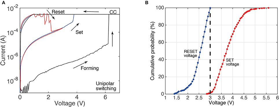
Figure 1. (A) Typical I/V curve for devices used in this study showing resistance switching in the unipolar mode. The current compliance limit is labeled as CC. (B) Cumulative probability plots of set and reset voltages obtained from more than 1,000 switching cycles (during the I/V sweeps).
Setting and Resetting Dependence on Pulse Shape
Devices may be set or reset depending on the shape of voltage pulses. Devices may be set by an ascending sequence of 300 ns voltage pulses, which, over a sufficiently long time, look like the leading edge of a voltage pulse, and then they may be reset in response to a descending sequence of pulses that look like the trailing edge of a triangular or sawtooth pulse. The gradual resistance change can be tracked by applying short read voltage pulses (0.6 V, 300 ns) that do not induce any switching (shown in in Figure 4). These pulses were applied in between each of the ascending or descending pulses that make up the sawtooth voltage ramp (Figures 2B,C—shown as a continuous blue line for clarity) while the current supplied by the Keithley system was measured, and hence the device resistance obtained. The transition from LRS to HRS begins to occur at around 2.7 V, a voltage that agrees well with the statistical measurements we carried out shown in Figure 2B. The ascending pulse train can then set the device to a LRS (Figure 2C). Resistance gradually decreases as the voltage bias increases, which demonstrates the system's capacity to exhibit plasticity. An important feature is that the resistance value for any SiOx device can be incrementally adjusted by controlling the initial resistance state, voltage starting position and cut-off voltage of the pulse train.
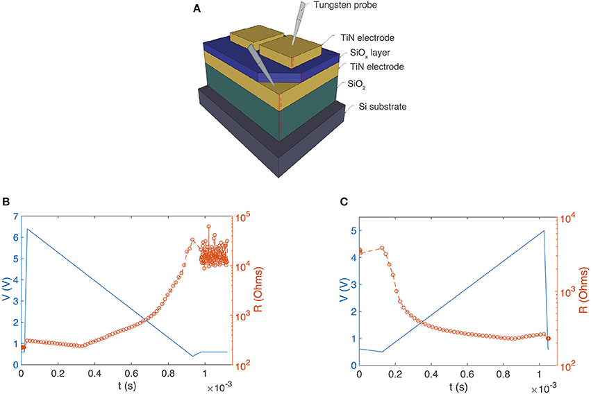
Figure 2. (A) Schematic illustration of a SiOx RRAM device (not to scale). TiN layers (electrodes) are 100 nm thick (yellow). The active SiOx layer is ~37 nm thick (blue). The gray needles represent tungsten probes. Controlling device resistance by SET and RESET with leading and trailing edges of voltage pulses. (B) Descending train of 300 ns voltage pulses (6.4–0 V: blue line for clarity) increases device resistance from ~100 Ω to ~20 kΩ (orange data points). (C) Ascending train of 300 ns voltage pulses (0–5 V: blue line for clarity) decreases device resistance from ~4 k to ~200 Ω (orange data points).
Spike-Timing Dependent Plasticity (STDP)
That the sign of voltage pulse gradient control both setting and resetting processes in our devices suggests that combining suitable tailored pulses and applying these to individual devices may allow us to emulate STDP in biological synapses. In this study, external circuitry is used to provide programming voltage pulses, but it should be borne in mind that they may in principle be generated by optimized unipolar devices, as we have previously demonstrated (Mehonic and Kenyon, 2016).
STDP is a form of Hebbian learning rule that results in synaptic modification based on the relative timing of pre- and post-synaptic voltage spikes (Hebb, 1949; Bi and Poo, 1998; Abbott et al., 2000; Jo et al., 2010). That is to say, the relative arrival time of two spikes (“pre-synaptic” and “post-synaptic”) at the synaptic gap determines whether the synaptic strength will be increased, decreased, or remain unaltered. The change of state in a biological synapse is represented the change in excitatory postsynaptic current amplitude; in a RRAM device this change is represented by the change in device conductance (Chua, 1971).
In order to control both setting and resetting processes we need to design suitable voltage pulses and to vary the delay between “pre-synaptic” and “post-synaptic” pulses. We chose two different combinations of pulse shape to test the STDP properties of our devices, with programming pulses being the sum of distinct pulses with variable inter-pulse delays. Figure 3 illustrates the concept of changing device conductance by tailoring pulse shape. In the first case, we used square and triangle pulses as the pre- and post-synaptic spikes, respectively (both 1.5 V, Figure 3A). To ensure that the transition point between setting and resetting is at zero the triangle pulse had different rise and fall times (Figure 3A). The leading edge of the triangle pulse was set to be equal to the duration of the square pulse. When the applied pulse, or combination of pulses, is below a threshold voltage, Vth, there is no change to the device conductance. However, for pulses above Vth, the device conductance will change dependent on the sequence of voltages applied to the device. In the case of a slowly rising pulse, the device will SET into a low resistance state once the threshold is reached. Rapidly reducing the voltage has little effect, and the device remains in the LRS. However, if the pulse has a sharp leading edge and a slow trailing edge, the integral of current flowing through the conductive filament can become high enough to generate sufficient Joule heating to rupture the filament. The device therefore enters the HRS. In Figure 4 we present an example of 12-cycle set of combined pulses for a non-identical pulse configuration. Each subsequent pulse has the delay between pre- and post-synaptic pulses reduced by 90 μs, and hence the resultant pulse shape changes from square followed by triangle to triangle followed by square. At intermediate delays we can see the device under test initially setting to a LRS and then resetting to a HRS. Device resistance is thus dependent on the time difference between the two pulses. As was predicted, a rising edge above Vth lowers the resistance of the device under test, while a gradually descending voltage edge above Vth increases it.
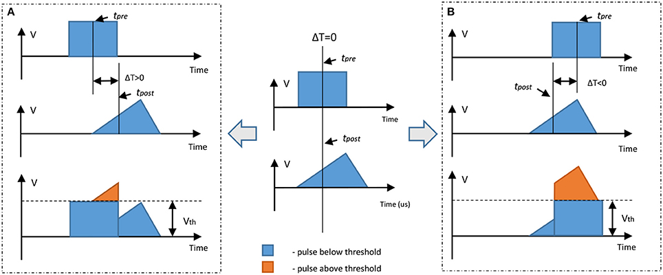
Figure 3. Illustration of a non-identical STDP-mimicking pulse set up. If a square pulse and a triangular pulse are below threshold there is no change in device resistance if a single pulse is applied; however, if the sum of these two pulses is above the threshold it is possible to adjust device resistance. In these examples the square pulse is a pre-synaptic spike and triangle pulse is a post-synaptic spike. (A) Pre-synaptic spike arrives earlier than the post-synaptic spike; the resulting sum is a slow leading edge above the threshold. This leads to decrease in resistance (increase in conductance—SET process). (B) The post-synaptic spike arrives earlier than the pre-synaptic spike; the resulting sum is a slow trailing edge above the threshold. This leads to an increase in resistance (decrease in conductance—RESET process).
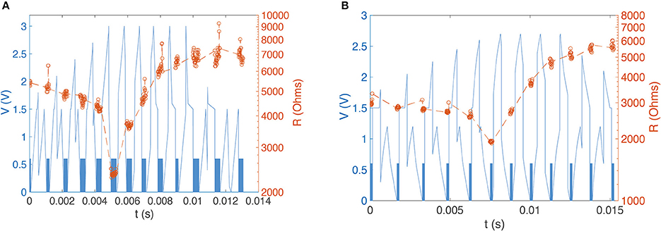
Figure 4. (A) Experimental device resistance measurements for a sequence of 12 programming pulses with varying pre-post (square-triangle) delays. Square 0.6 V 300 ns reading pulses (indistinguishable on this time scale, so present as a blue band) between shaped programming pulses yield 450 resistance measurements. We see clear evidence of potentiation and depression depending on programming pulse shape. (B) Experimental resistance measurement for a sequence of 11 pulses with varying pre-post delays in which the post-synaptic spike is altered with an emulated capacitor. We see again evidence of potentiation and depression.
In order to generate an STDP-like response with nominally identical pre- and post-synaptic pulses we used two square voltage pulses and modified the post-synaptic pulse with a capacitor; this is a scheme that may easily be implemented in a real system. Our previous work has demonstrated how voltage spikes can be generated by individual RRAM elements, and it would be straightforward to combine these with appropriate capacitive elements. The result is a modified square pulse that looks more like a triangular pulse. This allows us to exploit the previously-shown device response to different leading and trailing pulse edge slopes. To achieve the required gradient we emulated the response of a 3 μF capacitor, but it should be noted that much smaller capacitance values will be sufficient for devices operating in the nanosecond regime rather than the microsecond regime studied here for demonstration. The square pulse peak voltage remained the same at 1.5 V, and the pulse width was 450 μs. The shift that was previously required for a non-identical configuration was no longer needed due to the modification of the post-synaptic pulse. Figure 4B shows an example of a sequence of 11 pulses. The DUT shows similar behavior to the previous setup, and we are able to demonstrate that this pulse setup mimics biological STDP (Figure 5).
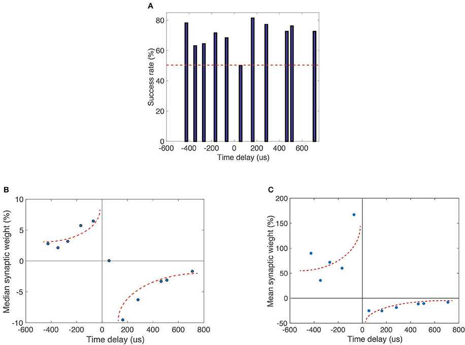
Figure 5. (A) Plotted percentage occurrence of expected operation (decrease or increase in conductance for negative and positive time delays, respectively) for 306 independent pulse sets. The occurrence rate is above 50% for most time difference configurations, indicating that expected operations are statistically favorable. (B) Median percent change in synaptic weight (conductance) vs. time delay between pre- and post-synaptic spikes for 306 independent identical pulse sets with 11 cycles in each set. (C) Mean percent change in synaptic weight (conductance) vs. time delay between pre- and post-synaptic spikes. Data were limited to events that were classified as successes in the statistical analysis shown in (A). Multiple memristive devices were used in this experiment. There is a distinct shape resemblance to biological STDP. Dotted lines are guides for the eye.
Statistical Analysis
We conducted a statistical analysis of the second pulse configuration (square pulse and modified square pulse). The results in Figure 5 are based on 306 pulse cycles identical to those represented in Figure 4. Before applying the pulse trains the devices were electroformed to a preconfigured resistance of ~2 kΩ. The pre-configuration routine is necessary to force a conductive filament into a metastable state whose conductance can be either increased or decreased by the appropriate voltage pulse combination. If the filament were in a very high resistance state, for example, further increases in resistance would not be possible. To investigate the statistical significance of timing-dependent changes in conductance, we determined the success rate of expected occurrences (Figure 5A). Here we measured for the same 306 pulse cycles the probability of a negative difference in pre- to post-synaptic pulse timing resulting in a positive change in synaptic weight (conductance), and vice-versa for positive differences in spike timing. We find that nearly all instances had a success rate >50%, indicating the statistical favorability of STDP-like behavior. The median of synaptic weight change (i.e., change in device conductance) is plotted against the relative time delay between pre- and post-synaptic pulses shows a striking similarity to biological STDP (Figure 5B). There is a transition at small positive delays that mimics biological behavior. Figure 5C shows the mean percent change in synaptic weight (conductance) versus time delay between pre- and post-synaptic spikes. In this case, we selected those instances of successful change in synaptic weight and constructed an STDP response curve. We have thus a proof-of-principle demonstration that not only it is possible to achieve STDP behavior, but also it is a statistically favorable process. We note at this point that the unsuccessful STDP events in our non-optimized devices are primarily related to the variability in set and reset voltages. This stochasticity may be greatly reduced through material optimization and device design, as we have recently demonstrated in RRAM devices for non-volatile memory applications. We are therefore confident that further work will improve substantially the success rates demonstrated here.
Conclusion
We have shown that it is possible to achieve an STDP response from unipolar SiOx RRAM devices. Furthermore, we have demonstrated that STDP behavior is a statistically favorable occurrence, even in non-optimized devices. This extends and adds to our previous work showing spiking, integration and thresholding in unipolar SiOx RRAM devices (Yu et al., 2011), and allows us to speculate that such devices can be used in hardware spiking neural networks to mimic a broad range of rich neuronal behavior, greatly simplifying the design of hardware neuromorphic systems. Further work is certainly required to establish design rules around neuromorphic systems based on RRAM devices, and the work we report is very much proof-of-concept at this stage. In particular, work is required to determine the flexibility of RRAM devices in terms of control they offer over metrics such as spiking frequency, power dissipation, conductance, and so on. We know from previous work that the electrical response of RRAM devices can be tailored through appropriate programming—particularly by the initial electroforming step—but work is needed to explore the limits of this approach. Further work is also needed to optimize both material and device structure to increase reliability. Nevertheless, combined with excellent CMOS compatibility, silicon oxide unipolar memristive devices are an interesting prospect for future neuromorphic systems.
Author Contributions
KZ: Performed the STDP experiments, designed the study, interpreted the data, and wrote the first draft of the manuscript; AM: Assisted in designing the study, interpreted the data, and assisted with drafting the manuscript; LM and MB: Assisted with experimental design and measurement; SH: Assisted with experiments; AK: Oversaw the work, co-designed the study, and assisted with interpreting the results; All authors contributed to the manuscript.
Funding
We gratefully acknowledge financial support provided by the Engineering and Physical Sciences Research Council (EPSRC). AM gratefully acknowledges the Royal Academy of Engineering and the funding provided through the Research Fellowship “Next Generation Adaptive Electronics for Neuromorphic Engineering”.
Conflict of Interest Statement
The authors declare that the research was conducted in the absence of any commercial or financial relationships that could be construed as a potential conflict of interest.
References
Abbott, L. F., Song, S., and Miller, K. D. (2000). Competitive Hebbian learning through spike-timing-dependent synaptic plasticity. Nat. Neurosci. 3, 919–926. doi: 10.1038/81453
Ambrogio, S., Balatti, S., Nardi, F., Facchinetti, S., and Ielmini, D. (2013). Spike-timing dependent plasticity in a transistor-selected resistive switching memory. Nanotechnology 24:384012. doi: 10.1088/0957-4484/24/38/384012
Ananthanarayanan, R., Esser, S., Simon, H., and Modha, D. (2009). “The cat is out of the bag: cortical simulations with 109 neurons, 1013 synapses” in Proceedings of 2009 IEEE/ACM Conference High Performance Networking Computing (Portland).
Bi, G. Q., and Poo, M. M. (1998). Synaptic modifications in cultured hippocampal neurons: dependence on spike timing, synaptic strength, and postsynaptic cell type. J. Neurosci. 18, 10464–10472.
Chen, H. Y., Yu, S., Gao, B., Huang, P., Kang, J., and Wong, H.-S. P. (2012). “HfOx based vertical resistive random access memory for cost-effective 3D cross-point architecture without cell selector,” in 2012 International Electron Devices Meeting, 20.7.1–20.7.4. San Francisco.
Chua, L. (1971). Memristor-The missing circuit element. IEEE Trans. Circ. Theory 18, 507–519. doi: 10.1109/TCT.1971.1083337
Indiveri, G. (2000). Modeling selective attention using a neuromorphic analog VLSI device. Neural Comput. 12, 2857–2880. doi: 10.1162/089976600300014755
Indiveri, G., Chicca, E., and Douglas, R. (2006). A VLSI array of low-power spiking neurons and bistable synapses with spike-timing dependent plasticity. IEEE Trans. Neural Netw. 17, 211–221. doi: 10.1109/TNN.2005.860850
Indiveri, G., Linares-Barranco, B., Hamilton, T. J., van Schaik, A., Etienne-Cummings, R., Delbruck, T. S., et al. (2011). Neuromorphic silicon neuron circuits. Front. Neurosci. 5:73. doi: 10.3389/fnins.2011.00073
Indiveri, G., Linares-Barranco, B., Legenstein, R., Deligeorgis, G., and Prodromakis, T. (2013). Integration of nanoscale memristor synapses in neuromorphic computing architectures. Nanotechnology 24:384010. doi: 10.1088/0957-4484/24/38/384010
Izhikevich, E. M., and Edelman, G. M. (2008). Large-scale model of mammalian thalamocortical systems. Proc. Natl. Acad. Sci. U.S.A. 105, 3593–3598. doi: 10.1073/pnas.0712231105
Jo, S. H., Chang, T., Ebong, I., Bhadviya, B. B., Mazumder, P., and Lu, W. (2010). Nanoscale memristor device as synapse in neuromorphic systems. Nano Lett. 10, 1297–1301. doi: 10.1021/nl904092h
Le Masson, G., Renaud-Le Masson, S., Debay, D., and Bal, T. (2002). Feedback inhibition controls spike transfer in hybrid thalamic circuits. Nature 417, 854–858. doi: 10.1038/nature00825
Mehonic, A., Buckwell, M., Montesi, L., Garnett, L., Hudziak, S., Fearn, S., et al. (2015). Structural changes and conductance thresholds in metal-free intrinsic SiOx resistive random access memory. J. Appl. Phys. 117:124505. doi: 10.1063/1.4916259
Mehonic, A., Buckwell, M., Montesi, L., Munde, M. S., Gao, D., Hudziak, S. J., et al. (2016). Nanoscale transformations in metastable, amorphous, silicon-rich silica. Adv. Mater. 28, 7486–7493. doi: 10.1002/adma.201601208
Mehonic, A., Cueff, S., Wojdak, M., Hudziak, S., Jambois, C., Labbé, O., et al. (2012a). Resistive switching in silicon suboxide films. J. Appl. Phys. 111:074507. doi: 10.1063/1.3701581
Mehonic, A., Cueff, S., Wojdak, M., Hudziak, S., Labbe, C., Rizk, R., et al. (2012b). Electrically tailored resistance switching in silicon oxide. Nanotechnology 23:455201. doi: 10.1088/0957-4484/23/45/455201
Mehonic, A., and Kenyon, A. J. (2015). “Resistive switching in oxides,” in Defects at Oxide Surfaces, eds J. Jupille and G. Thornton (Cham: Springer International Publishing), 401–428.
Mehonic, A., and Kenyon, A. J. (2016). Emulating the electrical activity of the neuron using a silicon oxide RRAM cell. Front. Neurosci. 10:57. doi: 10.3389/fnins.2016.00057
Mehonic, A., Munde, M. S., Ng, W. H., Buckwell, M., Montesi, L., Bosman, M. A. L. A. J., et al. (2017). Intrinsic resistance switching in amorphous silicon oxide for high performance SiOx ReRAM devices. Microelectr. Eng. 178, 98–103. doi: 10.1016/j.mee.2017.04.033
Mitra, S., Fusi, S., and Indiveri, G. (2009). Real-time classification of complex patterns using spike-based learning in neuromorphic VLSI. IEEE Trans. Biomed. Circuits Syst. 3, 32–42. doi: 10.1109/TBCAS.2008.2005781
Montesi, L., Buckwell, M., Zarudnyi, K., Garnett, L., Hudziak, S., Mehonic, A., et al. (2016). Nanosecond analog programming of substoichiometric silicon oxide resistive RAM. IEEE Trans. Nanotechnol. 15, 428–434. doi: 10.1109/TNANO.2016.2539925
Saïghi, S., Mayr, C. G., Serrano-Gotarredona, T., Schmidt, H., Lecerf, G., Tomas, J., et al. (2015). Plasticity in memristive devices for spiking neural networks. Front. Neurosci. 9:51. doi: 10.3389/fnins.2015.00051
Schacter, W. D., Gilbert, D. T., and Wegner, D. M. (2011). Psychology, 2nd Edn. New York, NY: Worth.
Serb, A., Bill, J., Khiat, A., Berdan, R., Legenstein, R., and Prodromakis, T. (2016).Unsupervised learning in probabilistic neural networks with multi-state metal-oxide memristive synapses. Nat. Commun. 7:12611. doi: 10.1038/ncomms12611
Smith, L. S. (2006). Handbook of Nature-Inspired and Innovative Computing: Integrating Classical Models with Emerging Technologies. New York, NY: Springer.
Strukov, D. B., Snider, G. S., Stewart, D. R., and Williams, R. S. (2008). The missing memristor found. Nature 453, 80–83. doi: 10.1038/nature06932
Torrezan, A. C., Strachan, J. P., Medeiros-Ribeiro, G., and Williams, R. S. (2011). Sub-nanosecond switching of a tantalum oxide memristor. Nanotechnology 22:485203. doi: 10.1088/0957-4484/22/48/485203
Vogelstein, R. J., Tenore, F. V. G., Guevremont, L., Etienne-Cummings, R., and Mushahwar, V. K. (2008). A silicon central pattern generator controls locomotion in vivo. IEEE Trans. Biomed. Circuits Syst. 2, 212–222. doi: 10.1109/TBCAS.2008.2001867
Waser, R., and Aono, M. (2007). Nanoionics-based resistive switching memories. Nat. Mater. 6, 833–840. doi: 10.1038/nmat2023
Yu, S., Gao, B., Fang, Z., Yu, H., Kang, J., and Wong, H.-S. P. (2013). A low energy oxide-based electronic synaptic device for neuromorphic visual systems with tolerance to device variation. Adv. Mater. 25, 1774–1779. doi: 10.1002/adma.201203680
Keywords: resistive switching, resistance switching, STDP, RRAM, machine learning, neuromorphic systems
Citation: Zarudnyi K, Mehonic A, Montesi L, Buckwell M, Hudziak S and Kenyon AJ (2018) Spike-Timing Dependent Plasticity in Unipolar Silicon Oxide RRAM Devices. Front. Neurosci. 12:57. doi: 10.3389/fnins.2018.00057
Received: 11 July 2017; Accepted: 23 January 2018;
Published: 08 February 2018.
Edited by:
Gert Cauwenberghs, Jacobs School of Engineering and Institute for Neural Computation, University of California, San Diego, United StatesReviewed by:
Sadique Sheik, BioCircuits Institute, University of California, San Diego, United StatesDuygu Kuzum, Department of Electrical and Computer Engineering, University of California, San Diego, United States
Copyright © 2018 Zarudnyi, Mehonic, Montesi, Buckwell, Hudziak and Kenyon. This is an open-access article distributed under the terms of the Creative Commons Attribution License (CC BY). The use, distribution or reproduction in other forums is permitted, provided the original author(s) and the copyright owner are credited and that the original publication in this journal is cited, in accordance with accepted academic practice. No use, distribution or reproduction is permitted which does not comply with these terms.
*Correspondence: Anthony J. Kenyon, YS5rZW55b25AdWNsLmFjLnVr